ABSTRACT
ZHANG, CHI. High Power Density High-Temperature Liquid Cooled SiC Inverter System. (Under the direction of Dr. Lukic).
Two SiC-based high power density electric vehicle (EV) traction inverter systems are developed in this thesis. The first system is capable of operating continuously at 105℃ ambient temperature and 65℃ coolant temperature while delivering 100kW peak power for 20 seconds. Key components, like DC-link capacitors and busbar are designed and arranged to achieve a total 2.8L volume with 0.8 fill factor, which leads to 34kW/L power density. The second system is able to deliver 100kW continuous power and 196kW peak power. A total 3.2L volume leads to 61kW/L power density.
A practical switch loss model is firstly build based on device characteristics, like switching loss and conduction loss, to predict inverter losses at different operating conditions, like output power, device junction temperature and coolant temperature. The model also
specifies the required thermal resistance for the cooling system to achieve target output power at required coolant temperature. In addition, the methodology of building the model can be
extended and used for not only the traction inverter but also other power electronics devices. Design and testing approach for liquid cooling system, including thermal interface material and cold plate, is then proposed according to the inverter thermal model. The total thermal resistance including thermal interface material (TIM) under test is obtained by doing conduction losses test and the optimal TIM is selected. The approach can be extended and used for any thermal interface selection or comparison in thermal design. Thermocouples are
resistance optimization. RTD imbedded in the modules are measured to estimate the junction temperature.
DC link decoupling snubber circuit is usually placed close to the power switches in electric power converters to suppress voltage ringing on the devices. Generally, a capacitive snubber or an RC snubber are preferred due to their simplicity and effectiveness. A forth order equivalent circuit is derived to analyze the thermal performance of both snubber circuits (C and RC) as well as their voltage suppression function. Thermal analysis and simulation results reveal that resistor in RC snubber can release the thermal stress on the capacitors, which makes the RC snubber more reliable at high switching frequency and high-power applications than a commonly used C snubber.
This thesis also presents a low-inductance dc busbar for silicon carbide-based electric vehicle traction inverters operating at high ambient temperatures. Unlike the laminated busbars, which use parallel copper sheets to establish low-inductance connection between the dc-link capacitor bank and all the switching devices, the proposed busbar uses capacitor sections which are vertically mounted on top of each power semiconductor module. This significantly reduces the busbar’s parasitic inductance and eliminates the unreliable snubber circuit which is typically used with laminated and PCB busbars to reduce the overvoltage spikes across the fast-switching semiconductor devices during the device turn-off transients.
© Copyright 2019 by Chi Zhang
High Power Density High-Temperature Liquid Cooled SiC Inverter System
by Chi Zhang
A thesis submitted to the Graduate Faculty of North Carolina State University
in partial fulfillment of the requirements for the degree of
Doctor of Philosophy
Electrical Engineering
Raleigh, North Carolina 2019
APPROVED BY:
_______________________________ _______________________________ Dr. Srdjan Lukic Dr. Iqbal Husain
Committee Chair
ii
DEDICATION
iii
BIOGRAPHY
iv
ACKNOWLEDGMENTS
I would like to dedicate my deepest gratitude to my advisor, Dr. Srdjan Lukic, for his guidance to my research work and his support in the past years of my Ph.D. study. I also
v
TABLE OF CONTENTS
LIST OF TABLES ... x
LIST OF FIGURES ... xii
I. Introduction ... 1
II. High Power Density Design ... 9
A. SiC Module ... 9
B. DC-link Capacitors ... 10
1. Requirement ... 10
2. Ceramic capacitors ... 11
3. Electrolytic capacitors ... 11
4. Film capacitors ... 11
5. Capacitor comparison ... 13
6. Capacitor self-heating calculation ... 14
C. High Temperature Controller Design ... 14
1. Components selection ... 14
2. PCB layout ... 15
3. Thermal test ... 16
D. Current Sensors ... 17
vi
F. Cold Plate ... 18
G. Busbars Design ... 19
H. Total Volume ... 20
III. System Thermal Design ... 22
A. Device Thermal Model ... 22
B. PLECS Simulation ... 23
C. MOSFETs Antiparallel Diode Losses ... 25
D. Inverter Power Losses Model ... 26
E. Junction Temperature Operation Points ... 29
F. Required Thermal Design ... 31
G. Inverter Thermal Model ... 32
H. Thermal Interface Material ... 32
1. TIM candidates ... 33
2. Rds,on recalibration ... 34
3. Conduction test ... 36
4. Testing results ... 38
5. Stencil ... 39
I. Thermocouple Implementation on Cold Plate ... 40
1. 1 mm slots cold plate ... 40
vii
J. Thermocouple Implementation on Baseplate ... 43
1. Module characterization ... 43
2. EDM process ... 44
3. Module tests after the EDM process ... 45
4. Milling slots with diamond saw ... 46
K. Thermal Modelling- Total Thermal Resistance ... 46
L. Thermal Modelling- Each Thermal Interface ... 47
M. Updated Expected System Performance ... 49
IV. Snubber Design ... 51
A. Loop Inductance ... 51
1. Double pulse test ... 51
2. Q3D extractor ... 52
B. C Snubber Optimization ... 54
C. Testing Failure and Analysis ... 55
D. Capacitors Thermal Tests ... 57
E. Snubber Circuit Analysis ... 58
1. Double-pulse circuit with a snubber circuit ... 58
2. High frequency equivalent circuit ... 59
3. Snubber capacitance and voltage spike ... 60
viii
5. Snubber capacitors losses with snubber resistor ... 63
6. Thermal performance ... 63
F. Cooling Copper Bar ... 64
V. Low Loop Inductance Busbar Design ... 66
A. Snubberless Operation ... 66
B. Low Loop Inductance Busbar Design ... 66
C. Q3D Simulation ... 68
D. Double Pulse Test ... 69
E. System with Low Loop Inductance Busbar ... 72
VI. System Construction and Experiment Results ... 74
A. Liquid Cooling System ... 74
1. Proposed cooling loop ... 74
2. Liquid cooling system ... 74
B. Load Bank and Inductor ... 76
C. Experiment Results ... 77
1. Testing bench ... 77
2. 100kW test ... 78
3. Thermal analysis ... 80
4. Voltage spike suppression ... 82
ix
1. Testing bench ... 83
2. 100 kW continuous test ... 85
3. 130 kVA test ... 87
4. 800V 196 kVA test ... 90
x
LIST OF TABLES
Table 1. Project Targets ... 5
Table 2. SiC Modules ... 9
Table 3. DC-link Capacitors Requirement ... 10
Table 4. DC-link Capacitors Comparison ... 13
Table 5. Key components on control board ... 15
Table 6. HAH3DR_700-S01 ... 17
Table 7. Cold plate comparison ... 18
Table 8. Symbols Definition ... 22
Table 9. PLECS Simulation Parameters ... 25
Table 10. Simulated Inverter Power Losses ... 27
Table 11. System performance estimation ... 31
Table 12. TIM Candidates ... 33
Table 13. Total Thermal Resistance ... 47
Table 14. Key poison temperatures ... 48
Table 15. Interface thermal resistance ... 49
Table 16. Updated expected system performance ... 50
Table 17. Estimated Loop Inductance ... 53
xi
Table 19. Measurements in data acquisition ... 75
Table 20. Components temperature in 105℃ test ... 81
Table 21. Experimental and simulated inverter thermal performance ... 82
Table 22. Components’ temperature measurements ... 86
xii
LIST OF FIGURES
Figure 1. High temperature film capacitors in development ... 12
Figure 2. Automotive packaged film capacitors ... 12
Figure 3. TDK 125C film capacitors ... 13
Figure 4. HT control board layout ... 15
Figure 5. Hot spot on the DSP ... 16
Figure 6. Gating signals at 105 °C ambient temperature ... 16
Figure 7. HAH3DR_700-S01 ... 17
Figure 8. AMPHENOL Power Connectors ... 18
Figure 9. Inverter layout design ... 20
Figure 10. Volume Distribution ... 21
Figure 11. Switching Losses Model ... 23
Figure 12. Conduction Losses model ... 23
Figure 13. PLECS. Simulation Schematic ... 24
Figure 14. Surface of Single Switch (half module) Losses ... 28
Figure 15. Cooling Power Surface ... 30
Figure 16. Intersections of power losses surface and cooling power surface ... 31
Figure 17. Inverter thermal model ... 32
xiii
Figure 19. Power supplies and meters for Rds,on recalibration ... 35
Figure 20. Vds and Id for Rds,on calibration ... 35
Figure 21. Rds,on vs junction temperature ... 36
Figure 22. Module on a heatsink for conduction losses test ... 37
Figure 23. Second approach for TIMS test ... 38
Figure 24. TIM testing results ... 39
Figure 25. Stencil and thermal grease on the module applied with stencil ... 39
Figure 26. Stencil Testing ... 40
Figure 27. Nine of 1.0mm slots on the cold plate ... 40
Figure 28. Thermocouples in the slots with epoxy ... 41
Figure 29. Thermocouples on the cold plate after treated in vacuum chamber ... 41
Figure 30. Thermocouples implementation on cold plate ... 42
Figure 31. Thermocouples measurements after implementation ... 42
Figure 32. 1.0mm vs 1.5mm slots cold plate ... 43
Figure 33. Double pulse test before any process on baseplate ... 44
Figure 34. EDM processed Module ... 45
Figure 35. Failed module due to EDM process ... 45
Figure 36. Thermocouples implemented on module baseplate ... 46
Figure 37. Temperature distribution ... 48
xiv
Figure 39. Busbar imported in Q3D Extractor ... 53
Figure 40. C snubber optimization ... 54
Figure 41. Double Pulse Test with 0.6uF snubber capacitor ... 54
Figure 42. Damaged modules ... 55
Figure 43. Last moment waveform ... 56
Figure 44. Simulated module failure ... 56
Figure 45. C snubber circuits (benchmark, TDK Ceramic, TDK film and pulse discharge) ... 57
Figure 46. High temperature capacitors testing results ... 58
Figure 47. Circuit diagram of a double-pulse circuit with a snubber circuit ... 59
Figure 48. High frequency equivalent circuit. ... 60
Figure 49. Voltage spike for different resistance at different snubber capacitance ... 61
Figure 50. Eergy loss of the snubber capacitor at different current ... 62
Figure 51. Energy loss on RC snubber circuit ... 63
Figure 52. Thermal measurement at 350V 50kW testing ... 64
Figure 53. Designed Copper Plate for snubber resistors ... 64
Figure 54. Copper plate implementation ... 65
Figure 55. Proposed low inductance busbar design ... 67
Figure 56. Capacitor section on new busbar ... 68
Figure 57. Loop inductance simulation model in Q3D ... 68
xv
Figure 59. Double pulse waveform at 300V 400V. ... 70
Figure 60. Double pulse waveform at 600V 300A ... 71
Figure 61. Double pulse waveform at 800V 400A ... 71
Figure 62. Unpackaged inverter system with low loop inductance busbar ... 72
Figure 63. Packaged inverter system ... 73
Figure 64. Proposed cooling loop diagram ... 74
Figure 65. Improved cooling system ... 75
Figure 66. Load banks ... 76
Figure 67. AC output inductors ... 76
Figure 68. Top view of inverter in chamber ... 77
Figure 69. Side view of inverter in chamber ... 78
Figure 70. 75℃ ambient test ... 79
Figure 71. 105℃ ambient test ... 80
Figure 72. Waveform at 100kW test ... 82
Figure 73. Voltage spike with/without snubber ... 83
Figure 74. New inverter in the chamber ... 84
Figure 75. New inverter with gate driver and controller ... 84
Figure 76. Key waveform at 100kW continuous test ... 85
Figure 77. Efficiency measurement at 100 kW test ... 86
xvi
Figure 79. Key waveform at 130kVA ... 88
Figure 80. Power Analyzer Image at 130kVA ... 89
Figure 81. Waveform for 800 V 196 kVA test ... 91
1
I.
Introduction
Modern power electronics converters are widely used in electric vehicles (EVs) to drive the electrical machines and to provide different voltage levels from the EV battery [1].Recently, the silicon carbide power semiconductor has been confirmed to be an attractive alternative which can push the limits of silicon devices. Compared with traditional Si-based power converters, the SiC-based have the potential for reliable operation at higher junction temperatures, higher switching frequencies, higher efficiency, and higher power densities [2].
For a power electronics converter, a sufficient temperature difference between the semiconductor junction and the coolant has to be achieved to remove the heat dissipated by the power semiconductor devices during the operation. As the junction temperature of Si
semiconductors is typically subjected to an upper temperature limit of 150℃, the converter output power is then limited by the insufficient temperature difference. In contrast, SiC
semiconductors are usually capable of operating at significantly higher operating temperatures of theoretically to 400℃ and of practically to at least 175℃ [3]. Thus, higher operating junction temperature with SiC-based semiconductor allows more output power from the converter.
SiC-based semiconductor even makes it feasible for the traction inverter operating in hot environments with pure air-cooling system. By placing the inverter close to the engine hood with up to 105℃ ambient temperature, the overall air-cooled traction inverter system complexity and cost can be reduce compared to the liquid-cooled system. The design of a 120℃ ambient
2 therefore, restricts the total inverter power level. An air-cooled 55-kW power inverter operating in 120℃ ambient temperature is designed and analyzed with dedicated air-cool system [5]. Due to the bulky heatsink in the air-cooled system, the power density is sacrificed. A large volume and heavy inverter can further increase the burden to the existing compact traction system in the Hybrid EVs. Placing the inverter system behind the rear seat can ensure a low ambient air temperature level, like Honda Civic [6], which makes very compact air-cooled inverter possible, [7], [8]. A SiC-Based high power density inverter operating at room temperature is developed based on a customized light-weight SiC-MOSFET power module, where the copper heat sink is directly soldered to the copper base plate of substrate [9]. Because high frequency switched voltage and current require to be transmitted for a long distance in the car from inverter to the mechanical system, this design could potentially cause electromagnetic interference (EMI) issue besides the losses during the power transmission. On the other hand, the total thermal resistance from power devices junction to the ambient in air-cooled system is usually much larger than the resistance of liquid-cooled system. In other words, much less heat can be removed by air-cooled system for the same given temperature difference from junction to the coolant, thus leading to much less power delivered to the electrical machine. Therefore, air-cooled system is not feasible for low volume high power traction inverter system.
3 save the cost and reduce the complexity. In [11], a 110 kVA inverter has been tested with coolant of different temperatures and the result shows substantially reduced output power with high-temperature coolant. In fact, due to the limitation of packaging technology, the maximum junction temperature of commercially available SiC power devices is typically set to 175℃, meaning the temperature difference from junction to coolant will be less than 70℃, which then affects the inverter performance, [12]. Therefore, this thesis will still implement the conventional 65℃ coolant cooling system, meanwhile investigate the limit of existing commercially available SiC devices in traction inverter system. The approaches and concepts discussed in this thesis can still be used in future when higher junction SiC devices become available in the market.
In EV system, the weight and volume of the automotive components are other key parameters we should pay attention to when designing the inverter system. In particular, for Hybrid EV system which already includes the conventional traction system, the additional volume and weight introduced by power electronics converters should not affect the original performance of the EV system. In other words, the advantage of hybrid EVs, like high mileage per gallon, should not be affected by the weight and volume of extra electrical parts. Considering the fact that the EV battery already contributes a significant portion, it becomes more critical to further shrink the size and reduce the weight of the on-board power electronics, like the traction inverter system. Thus, the department of energy requires the traction inverter to meet the target of 13.4kW/L and 14.1 kW/kg by 2022, [13].
4 frequency AC current demand makes it necessary to have power devices of high switching frequency to generate the desired sinusoidal output current with less harmonic content, which can reduce the losses in the machine.
Therefore, high power, low volume, liquid-cooled, high switching frequency Sic-based traction inverter is preferred in modern EV system. Some previous works already put efforts on some of these aspects. A 34kW/L three-phase SiC inverter is developed at 100 kHz switching frequency for room ambient operation [15]. In [16], authors report a design and experimental verification of a 200 kVA traction inverter using 900V, 2.5m, SiC power modules. The
overdesigned DC-link capacitors and the non-optimized busbar lead to very low power density even with liquid cooling system. A compact 110 kVA, 140℃ ambient,105℃ liquid cooled, SiC traction inverter is claimed to achieve a volumetric and gravimetric power density of 23.1 kVA/L and 16.8 kVA/kg, respectively [11]. Unfortunately, the majority components in this system are not be able to operate at140℃ ambient, thus an additional air cooling is required to keep the
enclosure inside ambient temperature below105℃. In [17] and [18], a 30kVA SiC MOSFET inverter is designed and evaluated for 180℃ ambient temperature operations. However, the switching devices require complicated cooling system design to dissipate the heat to the coolant, thus high-power-density was not the priority in this design. Additionally, not all the components were designed to operate at high temperature, which is required when both active and passive devices in automotive converters operate in high-temperature ambient.
5 continuously and 100 kW peak for 20 seconds, which meets the existing and even next
generation EV output power target. By using conventional 65℃ coolant, the developed inverter can be easily implemented in most existing EVs without any modification to the cooling system. The 40 kHz switching frequency can potentially cover the typical electrical machines for EVs and at same time reduce the passive components in the EV system, like the passive filter.
SiC MOSFETs are widely used in next generation power devices mainly because of their ability to operate at high switching frequency and high temperature, and for their low switching losses. However, fast switching causes voltage spike and ringing due to the resonance between the loop inductance and the parasitic capacitance of the switches. The voltage spike could damage the switching devices and introduce severe electromagnetic compatibility (EMC) problems, especially in high-frequency and hard-switching converters.
Table 1. Project Targets
Typically, the snubber circuits in form of decoupling capacitors are placed close to the power modules to suppress the overvoltage spikes and ringing. Decoupling capacitors are easy to implement and do not slow down the switching speed [19]. The effect of decoupling capacitors is analyzed in the frequency domain and quantifiable results independent of the device’s switching speed is derived, [19]. By carefully designing the snubber capacitance, the snubber can also improve the EMI in voltage source converters [20]. On the other hand, an RC snubber is also
Requirements Target
Switching frequency (kHz) 40
Continuous power for over 60 seconds (kW) 60 Maximum power for 20 seconds (kW) 100
Operating voltage (Vdc) (285-425 V) nom. 325 V
Target power density (kW/L) > 30
Target efficiency (%) 98
Cooling Liquid-cooled with 65°C coolant
6 easy to apply and can provide an effective level of ringing suppression. In [21], an analytical technique based on the root locus method for designing a RC snubber for converters with phase-leg configurations is proposed. The author proposed to eliminate the loop inductance from the switching device to the snubber circuit to simply a fourth-order problem to third-order, which is not reasonable because it’s this loop inductance which results in the voltage spike during the transient. Therefore, this thesis will analyze snubber circuit performance numerically based on a detailed forth-order high-frequency equivalent circuit without eliminating the key components.
On the other hand, the analyses and designs in [19]-[21] are proposed only in terms of voltage spike suppression or EMI improvement and there is no discussion about the thermal performance of these snubber circuits in high-power applications with the devices operating at high switching frequencies. Since the SiC-based converters are becoming more attractive in high ambient temperature applications (e.g. 105℃ or higher [22][23]), the thermal properties of snubber circuits need to be re-evaluated and quantified in more detail to be suitable for use with these new devices. In these applications, the non-optimal thermal performance of the passive components (mainly capacitors) can become a significant limiting factor and even lead to the system failure and loss of the switching devices. This especially applies to the snubber circuit which are subjected to high thermal stress caused by high-frequency ripple currents carried by the snubber. Therefore, the thermal properties of snubber circuits must be carefully evaluated before the final design is applied in the system using new SiC devices and operating at elevated ambient temperatures. In this thesis, a practical snubber optimization approach will be discussed for both voltage spike suppression and thermal performance.
7 dc-link capacitors to the semiconductor devices, with a thin layer of insulating material between them. This type of busbar arrangement can typically achieve parasitic loop inductance of 20-50 nH [5]. The parasitic loop inductance of the laminated busbar causes overvoltage spikes between semiconductor device's terminals as a result of a very fast decrease of electric current through the busbar system, and it is directly proportional to the loop inductance.
The overvoltage spike can introduce severe electromagnetic compatibility (EMC) problems and even exceed the device's breakdown voltage and destroy the device. This is especially critical when fast SiC power MOSFETs are used. If the total inductance in the current path is not small enough to avoid overvoltage spikes, an additional snubber circuit is typically used. This additional circuitry can create system reliability issues in high-power inverters operating at high ambient temperatures, since it dissipates significant amount of heat and the ceramic capacitors (which are typically used) tend to overheat and fail short. It is therefore critically important to have the busbar parasitic inductance as small as possible to avoid using these decoupling capacitors when fast SiC power devices are used in high-power inverters. The PCB-based busbars [29]-[30] offer loop inductance in the range of 10 nH and enable higher power density, but the system still needs local decoupling capacitors (which are typically ceramic) to reduce the overvoltage spikes during the turn-off transients.
In Section II, the inverter system design in detail from the selection of key components and their arrangement aiming to achieve high power density are discussed. Inverter thermal design including inverter losses analysis, power device junction temperature calculation, and thermal interface material design is discussed in section III. In section IV, we firstly apply a conventional snubber circuit and find its limitations. Later, a fourth-order high-frequency
9
II.
High Power Density Design
A.
SiC Module
When the inverter was designed at the beginning, there were limited number of SiC MOSFETs modules in the market. Table 2 lists the candidates for the inverter, which are provided by WOLFSPEED, ST and ROHM. Considering the high current ability, small
switching losses, the SiC module CAS325M12HM2 from WOLFSPEED is selected as inverter switching devices.
Table 2. SiC Modules
Transistor Package
ID [A]
TJ = 175 °C
VDS [V]
ID = 250
A
EON [mJ]
VDS =
600 V ID = 250
A
EOFF
[mJ] VDS =
600 V ID = 250
A RthJC [K/W] Wolfspeed CAS325M12HM2 Half-Bridge 256@Tc= 125 °C, 424 @Tc= 25 °C 1.8 TJ = 175°C
5 3 0.11
APEI HT-3231-R (1.7kV) Half-Bridge 100 Tc = 150 °C, 5 TJ = 175°C
3.7 2.5 0.12
ST Microelectronics APTMC120TAM12CTPAG Triple phase leg 165 TC = 80°C
4.5 TJ = 150°C
5 3.5 0.135
ST Microelectronics APTSM120AM08CT6AG
Phase leg
290 TC = 80°C
3.2 TJ = 175°C
5.2 3.2 0.11
ROHM
BSM300D12P2E001
Half-Bridge
300 TC = 60°C
2.8 TJ = 150°C
8 8.5 0.11
ROHM
BSM180D12P2E002
Half-Bridge
204 TC = 60°C
5.2 TJ = 150°C
10
B.
DC-link Capacitors
1. Requirement
The DC-link capacitors are selected based on dc voltage, current ripple, and maximum allowable operating temperature, as well as the required capacitance.
The RMS current can be calculated given the modulation index, DC voltage and power factor.
2
3 3 9
2 cos 110
4 16 3 cos 2 out DC P
I m m A
V
Assuming 1-meter AWG 4/0 copper wire is used for the connection from the electrical vehicle batteries from the inverter, the self-inductance is estimated to be 1 uH according to Transmission Line Design Handbook by Brian C Wadell. In this case, 200 uF bus capacitance will make the cut-off frequency of the LC filter between EV batteries and inverter to be 11 kHz. This filter will prevent EV batteries suffering the 40 kHz ripple current.
On the other hand, the capacitors RMS current in PLECS simulation is 67 A at 60 kW and 110 A at 100 kW. Therefore, the target capacitors requirements are listed in Table 3.
Table 3. DC-link Capacitors Requirement
Parameters Target
Capacitance 200uF
RMS @ 40kHz 67A for 60kW, 110A for 100kW
11 2. Ceramic capacitors
Ceramic capacitors usually have high capacitance density and can operate at very wide ambient temperature from -40℃ to 150℃. For example, Kemet and AVX provide stacked ceramic capacitors up to 340μF for −55°C to +200°C ambient operation.
However, they usually have low capacitance per device due to their thick dielectric, leading to a high number of capacitors required at high power applications. Stacking many capacitors in parallel will increase the system cost significantly and can potentially reduce the reliability due to possible cracks induced by thermal stress.
3. Electrolytic capacitors
Electrolytic capacitors usually have large capacitance values with relatively low cost. However, the ESR and ESL of the electrolytic capacitors are usually much higher than those of ceramic capacitors and film capacitors, which will weaken the filter function of the DC-link capacitors and produce more losses. In addition, if electrolytic capacitors are selected, the system lifetime could be significantly reduced at elevated temperatures. For example, for TDK B43693 series capacitors, the lifetime would be reduced from 250k hours at room temperature to 2.5k hours at 105℃, which is not sufficient for automotive applications.
4. Film capacitors
12 Figure 1. High temperature film capacitors in development
On the other hand, Panasonic and TDK EPCOS provide automotive packaged film capacitors, which can be operated in 105℃ ambient temperature, Figure 2. These capacitors have been implemented in traction inverters and deliver high performance. However, their capacitances are usually optimized for low switching frequency (5-10 kHz) inverters and have much higher capacitance than required, which usually results in large volume. Therefore, using these capacitors could decrease the power density of the inverter design.
Figure 2. Automotive packaged film capacitors
13 Figure 3. TDK 125C film capacitors
5. Capacitor comparison
A comprehensive comparison of the discussed capacitors is shown in Table 4. Compared to the other candidates, the TDK 125°C Film has relatively small volume, better shape for high power density arrangement and better electrical performance.
Table 4. DC-link Capacitors Comparison
Therefore, sixteen (16) TDK B32776P film capacitors with a total capacitance of 192 μF, rated dc voltage of 600 V and a ripple current capability of 130 A at 105 ℃ are selected. The total volume of the 16 capacitors is approximately 0.55L.
Capacitors Capacitance/volta
ge/Irms @125°C Volume L Lifetime Price
TDK Film 600uF/450V/150A 0.5 >15000h@1
05°C
$877
TDK Ceramic 0.47uF/630V/N/A 0.07 N/A $1500
Chemi-con Ceramic
1.2uF/500V/1A 0.1 N/A $688
TDK 125°C Film 12.0uF/700V/12A 0.55 >50000h@1
14 6. Capacitor self-heating calculation
The temperature rise of the selected capacitors should be less than 20℃ to keep the inside temperature below 125℃ at 105℃ operation temperature. The dissipated power, Pdis (mW), is defined.
2 2
typ rms rms
(mW) ESR (m ) I (A ) 4.5 5.4 131.22 dis
P mW
Temperature difference is defined with equivalent heat coefficient G from datasheet. (mW) / (mW/ C) 131.22 / 58 2.26
dis
T P G C
Maximum allowed temperature difference is calculated where 0.7 factor at 105℃ is provided by the datasheet.
2 2
max(105C) Factor max(85C) 0.7 15 7.35 C
T T
Based on this result, the capacitors can safely operate at 105℃ for 100kW.
C.
High Temperature Controller Design
A high temperature controller is required for this inverter system to provide precise PWM signals to the gate drivers and process the sensing signals at 105℃ ambient temperature. All selected components can operate at 105℃ ambient temperature, and majority of them are either ACE -Q100 (integrated circuits) qualified or ACE-Q200 (passive components) qualified.
1. Components selection
15 ADC. Standard automotive CAN Bus Transceivers SN65HVD234-Q1 provides CAN link for communication to DSP.
Table 5. Key components on control board
Function Devices Temperature Range Max Junction
Temperature
DSP TI
TMS320F28377DPTPQ -40 to 125 °C 150 °C Non-isolated power
supply TI LMZxxx series -40 to 125 °C 150 °C
Digital isolator TI ISO7742FQ -40 to 125 °C 150 °C
Isolated amplifier TI AMC1301DWVR -40 to 125 °C 150 °C
2. PCB layout
The PCB board is shown below. The controller is placed in the middle for generating PWM signals and processing sensing signals. The DC-DC converters are located on the right side with the input 12V connection. On the right side, there are ADC sensing circuits for DC bus voltage and AC output current. PWM generation circuits are placed on the bottom with fault indicator LEDs.
16 3. Thermal test
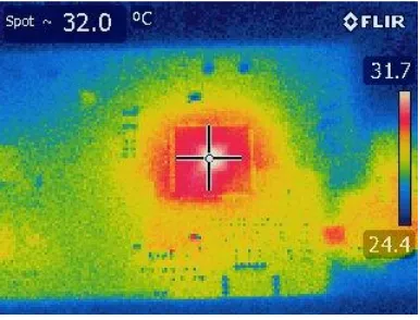
Control board operates at room temperature and the hottest spot located on the DSP is only about 8 °C higher than the ambient. Thus, we can expect less than 10 °C temperature rise at 105 °C ambient temperature.
Figure 5. Hot spot on the DSP
In addition, the control board is tested in the oven at 105 °C ambient temperature for 3 hours. The input power for the whole control board remains less than 1.2 W. The PWM gating signals are normal all the time, no pulse missing observed.
17
D.
Current Sensors
LEM provides high temperature current sensors for automotive applications, like the three phase traction inverters. Due to the compact design for sensing three phase current in only one unit, the HAH3DR_700-S01 is selected as the current sensor with specifications shown in Table 6.
Figure 7. HAH3DR_700-S01 Table 6. HAH3DR_700-S01
Function / Component Part number
Current sensor HAH3DR_700-S01
Parameter Value Unit
Measuring range (DC or RMS) -+700 A
Temperature Minimum temperature -50 ℃
Maximum temperature 125 ℃
Ambient temperature 105 ℃
Frequency bandwidth 40k Hz
Ratio metricity Error -+0.5 %
Sensitivity 2.86 mV/A
E.
Connectors
AMPHENOL INDUSTRIAL PowerLok Series is selected as inverter DC and AC output connectors due to its compact design, easy busbar-type mounting, up to 300A continuous current ability, 1000V insolation voltage, and -40 – 125 °C operation range. In addition, they are
18 Figure 8. AMPHENOL Power Connectors
F.
Cold Plate
To achieve as small as possible total thermal resistance, the cold plate should have good performance of absorbing the heat from the modules. On the other hand, the cold plate should be as compact as possible to obtain the target power density because the cold plate usually takes significant space in a liquid-cooled converter. Based on these two guidelines, the flowering two cold plates in the market are selected in Table 7. Compared to the CP 3009, 007-MXQ-01 cold plate has lower thermal resistance, lower pressure drop and smaller total volume, thus is selected as the inverter cold plate. Its thermal performance will be further examined in later chapters.
Table 7. Cold plate comparison
Cold Plate MICROCOOL CP 3009 007-MXQ-01
Thermal resistance @10L/min
from Spec 0.011C/W 0.0075C/W
Pressure Drop 1.9 PSI 1.75 PSI
CP Volume 0.75L 0.53L
Price 265 350
Implementation Wired shape, difficult to utilize the space below the plate
19
G.
Busbars Design
The current through the AC and DC busbars of a 100 kW three-phase inverter, can be calculated as below, where PF is the power factor and MI represents the modulation index. The conventional SPWM modulation scheme is applied.
DC in DC
I P V
(3 ) 2 (3 )
AC out ph out DC
I P V PF P V PF MI
Considering the high current-carrying requirements, the required wide operating
20 Figure 9. Inverter layout design
H.
Total Volume
21 Figure 10. Volume Distribution
0.2
0.55
0.214
0.55 0.77
0.05
0.2 0.266
Busbar
DC-link capacitor
Moduel
Cold Plate
Air
Current Sensor
Power Connector
22
III.
System Thermal Design
The symbols which will be used in the following chapters are defined in Table 8. Table 8. Symbols Definition
Symbol Definition
Tj Junction temperature
TCoolant Coolant Temperature
fs Switching frequency
Pcond Conduction losses
Pout Inverter continuous output power
Psw Switching losses
Ploss Signal Switch losses
Pcool Cooling power
Rth,total Total thermal resistance
Rth,JC Junction-to-Case thermal resistance
Rth,TIM Thermal Interface Material thermal resistance
Rth,plate Cold plate thermal resistance
A.
Device Thermal Model
After selecting the MOSFETs module, the detailed performance, like the conduction and switching losses at different conditions should be further examined in our inverter system. PLECS software is applied to simulate the behavior of the three-phase inverter and extract the thermal performance of the selected modules, due to its professional thermal simulation function.
23 voltage, current and junction temperature, based on the imported thermal model. Usually, the thermal model includes turn-on losses lookup table, turn-off losses lookup table and conduction losses lookup table. These tables can be built from the MOSFETs datasheet or more accurately by doing the double pulse test and conduction loss test. The initial thermal model in this design is established from datasheet, as shown Figure 11 and Figure 12.
Figure 11. Switching Losses Model
Figure 12. Conduction Losses model
B.
PLECS Simulation
24 current three-phase inductors in the lab are rated 75uH at 60Hz. Conventional SPWM
modulation method will be used in this application. The modulation index is determined by sine reference amplitude, which is designed to be 0.9 as a practical value. The other parameters are determined from the inverter requirements.
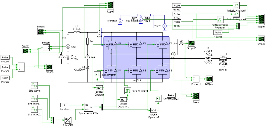
Figure 13. PLECS. Simulation Schematic
Six MOSFETs and their body diodes are placed on a heatsink (Blue rectangle), which will absorb the thermal losses dissipated by the components within its boundaries. At the same time, it defines an isotherm environment and propagates its temperature to the components which it encloses. In other words, the components on the heatsink share same operating temperature defined by the heatsink. One terminal of the heat sink is connected to an external thermal network, which represents the liquid cooling system and the coolant temperature. As we are more interested in the module losses at different junction temperature, the heatsink initial
25 Table 9. PLECS Simulation Parameters
The inverter output power can be calculated as blow, where cosθ represents the output power factor and m is the modulation index. By changing the resistive load, we can get different output power.
, ,
3 cos
out ph rms ph rms
P V I
,
1 2 2
ph rms DC
V m V
, / , , cos
ph ph rms ph rms ph ph
Z V I R Z
C.
MOSFETs Antiparallel Diode Losses
As the conventional SPWM modulation is applied, the switching device is always turned on when current is flowing through it, either forward current or reverse current, if deadtime is not considered. Therefore, whether the reverse current will go through MOSFETs or their
antiparallel diodes depends on the reverse current, Rds,on and diode threshold voltage. In our application, the critical current is calculated as 2.5 V/7.6 mOhm = 329A at 175°C junction temperature, where 2.5V is the diode threshold voltage and 7.6 mOhm represents the Rds,on at
Input DC voltage 400 V
DC-link capacitance 200 uF
MOSFETs CAS325M12HM2
Load Inductance (per phase) 75 uH
Load resistance (per phase) for 60kW 0.783 Ohm
Load resistance (per phase) for 100kW 0.47 Ohm
Sine Reference frequency 60Hz
Sine reference amplitude 0.9
26 175°C junction temperature. Therefore, no current will go through diode and no loss should show up in simulation theoretically for 60kW output power. As for 100kW, where the peak current goes up to 410A, the reverse current will flow through the diode rather than the
MOSFETs for a short period during each cycle. On the other hand, 500ns deadtime is considered and simulated in the PLECS, which will force reverse current to go through the diode for another short period. All these considerations have been simulated in the PLECS and the maximum power losses on antiparallel diode at 100kW is less than 5W, which is negligible compared to the MOSFETs losses. Therefore, we will no longer consider the diode losses in the further design.
As most of the reverse current will flow through the MOSFETs, the 3rd quadrant
characteristic of MOSFET module should be considered in simulation. MOSFETs thermal model shown in Figure 11and Figure 12 has already been modified with 3rd quadrant characteristic besides 1st quadrant characteristic.
D.
Inverter Power Losses Model
27 Table 10. Simulated Inverter Power Losses
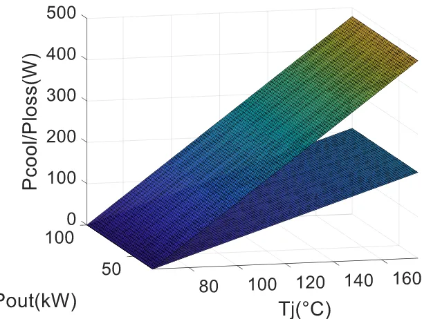
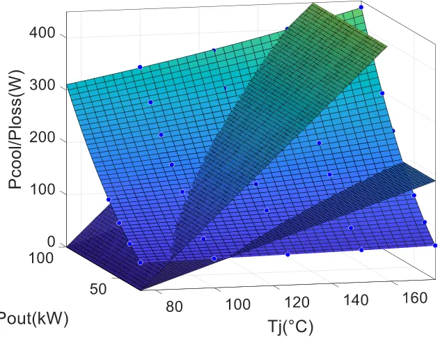
These raw data are imported into MATLAB and a loss surface in Figure 14 is generated by applying curve fitting tool. This figure shows that the losses are only depended on output power and the junction temperature and not related to the cooling system.
Note that the losses in the plot is only referring to one single switch (half module) rather than a module or the whole inverter. For three-phase inverter, it has total six switches. Thus, the total losses in our inverter is six times as the loss for one single switch. In the following report, only signal switch loss will be discussed unless other terms are specifically used.
P
out(kW) Irms(A)
P
cond(W)
P
sw(W)
25 °C 50°C 75°C 100°C 125°C 150°C 175°C
30kW 84.8 13.11 14.7 16.8 18.9 21.0 23.9 26.8 39.7
40kW 113.4 23.27 26.2 29.8 33.4 37.0 42.0 47.0 49.0
50kW 141.6 36.5 40.8 46.3 51.8 57.5 65.0 72.7 58.4
60kW 169.6 52.4 58.7 66.5 74.0 82.2 92.9 103.8 67.8
70kW 197.8 71.1 79.6 89.9 100.2 111.0 125.6 140.4 77.4
80Kw 225.8 92.5 103.5 116.8 130.0 143.9 162.8 181.9 87.0
90kW 254.4 116.7 130.4 147.2 163.8 181.1 205.0 229.3 97.2
28 Figure 14. Surface of Single Switch (half module) Losses
Based on previous simulation results, the conduction losses are only dependent on junction temperature and output power if other parameters are set, like the DC input voltage, modulation index. On the other hand, the switching losses are also only dependent on junction temperature and output power if switching frequency is set to 40 kHz. Therefore, the conduction losses and switching losses are two functions of Tj and P
out. The functions are dependent on the
device thermal model and other parameters which are already set in our design. Therefore, we can find the conduction losses and switching losses given T
j and Poutwhen the two functions are
known.
Usually, the loss functions are not linear and can’t not be easily obtained. The large signal and small signal analysis can provide us the inverter basic behaviors, but it requires massive calculations and still rely on the non-linear module thermal model to extract the losses.
29
3 2 2 2
3 2
3.94
6 *
2.74
5*
*
1.96
3*
8.53
5*
*
4.84
3*
*
0.252 *
5.1
6 *
0.0109 *
1.18*
2.64
loss j j out j j out
j out j out out out
P
e
T
e
T
P
e
T
e
T
P
e
T
P
T
e
P
P
P
E.
Junction Temperature Operation Points
In the design process of a power electronic converter, the junction temperature should never exceed the preset limit under any circumstances. In other words, the thermal operating point of the system should be designed to be in a safe and optimum range, which is given by the loss behavior of the switching devices and the cooling system. Based on the previous analysis, the inverter loss power can be expressed as a function of junction temperature and output power. Meanwhile, cooling power Pcool can also be defined as a function of junction temperature, input
coolant temperature TCoolant (or ambient temperature for air-cooled system) and total thermal
resistance Rth,total. These two powers should always be same at any steady state and the junction
temperature is determined when coolant temperature and total thermal resistance are given.
loss cond sw
P P P
,
( ) /
cool j A th total
P T T R
cool loss
P P
30 will be more heat cooled by the cooling system. For the system with lower thermal resistance, it can dissipate more power at same junction temperature.
Figure 15. Cooling Power Surface
When the power loss surface and the cooling surface are plotted together in the same ordinates in Figure 16, the intersections are the possible junction operation points. The
31 Figure 16. Intersections of power losses surface and cooling power surface
F.
Required Thermal Design
Table 11. System performance estimation
Based on the previous analysis, the system thermal performance can be predicted. The Table 11 shows the estimated system performance, where the 0.3 ℃/W is an estimated total thermal resistance from junction to coolant based on previous experience. If we expect the
Coolant Temperature
Junction Temperature
Continuous Power
Total
Losses Rth,total Efficiency
65 °C 108 °C 60 kW 864 W 0.3 °C/W 98.56%
65 °C 175 °C 96.6 kW 2200 W 0.3 °C/W 97.72%
65 °C 150 °C 86.6 kW 1700 W 0.3 °C/W 98.03%
65 °C 150 °C 100 kW 2152 W 0.23 °C/W 97.84%
65 °C 175 °C 100 kW 2330 W 0.28 °C/W 97.67%
65 °C 150 °C 110 kW 2525 W 0.2 °C/W 97.95%
32 system to deliver 100kW at 150℃ junction temperature, the thermal resistance should be at most 0.23℃/W, which is the thermal design baseline.
G.
Inverter Thermal Model
The thermal model of the inverter is illustrated in Figure 17. The total thermal resistance is the sum of MOSFETs junction-to-case thermal resistance Rth,JC, thermal interface material
(TIM) thermal resistance Rth,TIM and cold plate thermal resistance Rth,plate . Usually, the
junction-to-case thermal resistance is defined by the module package technique and can’t be modified if commercial MOSFETs module are used. In our application, the selected module typical Rth,JC is
0.1 ℃/W. Therefore, it’s very critical to select the TIM and the cold plate to obtain a desired total thermal resistance.
,
0.1
, ,th th JC th TIM th CP
R
R
C
W
R
R
Figure 17. Inverter thermal model
H.
Thermal Interface Material
The thermal interface material describes any material that is inserted between two parts in order to enhance the thermal coupling between these two components. Thermal grease is one example of the TIM and usually is a kind of thermally conductive compound. It is commonly
50% Ethylene Glycol Cooling
SiC Die
Direct Bond Copper / substrate Solder
Thermal Interface Material
Cold Plate
Tjunction
33 used as an interface between heat sinks and heat sources. The main role of thermal grease is to eliminate air gaps or spaces from the interface area to maximize heat transfer. The TIM plays an important role in accumulated thermal resistance and we must select the TIM with as small as possible thermal resistance.
1. TIM candidates
There are plenty of TIMs in the market and four of them are selected from different applications because of their high thermal conductivity in specifications in Table 12. Wakefield 126, which is very common in the lab, is selected as our benchmark. Thermal Grizzly is ranked as best thermal grease in 2015 on overclocking website. Newly released Fischerelektronik thermal grease comes from the high performance heatsink manufacture. Graftech provides samples of flexible graphite materials TIM (HT-C3200) with high thermal conductivity. Indium Heat-Spring has the highest thermal conductivity among them.
Table 12. TIM Candidates
TIM Silicone
based
Thermal
Conductivity Temperature Price $/Module
Wakefield 126
(Benchmark) NO 0.69 (W/m k) -40 to +200°C <1
Thermal Grizzly Yes 12.5 (W/m k) -200 to +350°C 3
Fischer WLPK NO 10.0 (W/m k) -60 to +150°C 1.5
Graftech HT-C3200 NO 7.00 (W/m k) -40 to +400°C N/A
34
Figure 18. TIM Candidates 2. Rds,on recalibration
To find the best TIM for our inverter, a simple but accurate testing approach is proposed in this report. The first step is to recalibrate the relationship between Rds,on and junction
temperature.
Although the Rds,on vs junction temperature curve is given in the datasheet, the curve varies from module to module. In addition, the Rds,on can be defined as chip level or module level. Chip level means the resistance on the die while module level represents the resistance including the module package. Thus, a recalibration is necessary for a specific module to get its
own Rds,on on the module level.
The module is placed in the chamber to have desired junction temperature. The voltage meter measures the drain-source voltage while the current meters measures the drain current. The module level resistance, therefore, can be expressed.
, , ,
/
ds on Tj ds Tj d
35 Figure 19. Power supplies and meters for Rds,on recalibration
The module is turned on all the time with a constant 18V gating signal. A current source provides desired drain current through the module. In order to eliminate the junction temperature rise due to the conduction losses, the drain current should be limited below 40A with less than 5W losses. It takes about 1.5 to 2 hours for the drain-to-source voltages to be stable in the oven. For each temperature, several drain-to-source voltages are measured to obtain the Rds,on. The slope in the plot represents the Rds,on (mOhm) and R-squared shows good linearity.
Figure 20. Vds and Id for Rds,on calibration
The measured resistance is about 0.3 mΩ higher than the curve from datasheet (red curve), which is mainly because the measured resistance includes connection resistance on the module level, whereas the datasheet provides only the resistance on chip level.
82 84 86 88 90 92 94
0 50 100
V
ds
(mV
)
36 Figure 21. Rds,on vs junction temperature
3. Conduction test
37 Figure 22. Module on a heatsink for conduction losses test
Although TIM thermal resistance is very difficult to measure separately, we can measure the total thermal resistance and keep other two resistance constant during the testing. Total thermal resistance can be calculated from power losses and temperature difference. In the test, ambient temperature and source current remain constant. Junction temperature can be obtained from Rds,on and the thermal resistance difference can be calculated as below, where ID represents the drain-source current, Ploss is the total conduction loss per switch and the junction temperature
Tj can be found based on the relationship just obtained.
, , , , , ,
th total i th JC th TIM i th CP
R R R R
2, , , , , , , , ,
th total i j i a loss i loss i ds i D ds on i D
R T T P P V I R I
2
2
, ,1 ,2 ,2 , ,2 ,1 , ,1
th TIM th th j a ds on D j a ds on D
R R R T T R I T T R I
Another easier and obvious way to compare the TIMs is to compare the drain-source voltage at same current. Conduction losses curve is plotted based on the relationship between
38 different cooling systems are plotted in the same coordinate, where ambient temperature is set to 25℃ (Yellow). The intersection represents the operating points. The better cooling system has smaller junction temperature, thus smaller drain-source. Because the other two thermal
resistances are constant, the smaller total thermal resistance, the better the TIM is.
Figure 23. Second approach for TIMS test 4. Testing results
Thermal Grizzly shows the best performance with the smallest total thermal resistance. However, silicone based thermal grease has tendency for the oil to physically migrate and separate from the solids, especially under high pressure. What’s worse, after several thermal cycles, silicone thermal grease can dry out. Thus, thermal grizzly is not suitable in our high temperature inverter design.
Fischer grease has the second least thermal resistance, therefore, it is selected as our TIM. The poor performance of Graftech and indium sheets probably results from low mounting
39 Figure 24. TIM testing results
5. Stencil
For consistency and repeatability, a stencil- or screen-printed TIM is recommended. Stencil can provide better control of a variable-volume deposit, where the final printed thickness of the grease can be altered to accommodate uneven surfaces. An optimum layer thickness will displace all air but will not prevent the metal-to-metal contact. Another advantage of a stencil is that less effort will be needed for cleanup.
Figure 25. Stencil and thermal grease on the module applied with stencil A stencil is made based on the CREE model and the thermal grease is applied with the stencil, Figure 25. The total thermal resistance with stencil is similar to that without stencil. No
0.18 0.19 0.2 0.21 0.22 0.23 0.24
Thermal Grizzly
Fischer Graftech Indium Benchmark
Total
Rth
40 obvious improvement with stencil is observed, Figure 26. Thus, stencil won’t be used in final design.
Figure 26. Stencil Testing
I.
Thermocouple Implementation on Cold Plate
To monitor cold plate surface temperature, and baseplate surface temperature, K-type thermocouples will be implemented.
1. 1 mm slots cold plate
Considering not to affect the thermal resistance of the cold plate, nine of 1.0 mm deep slots are milled on cold plate and the ends are right below the dies on the module.
Figure 27. Nine of 1.0mm slots on the cold plate
0.2 0.205 0.21 0.215 0.22
Fischer with Stencil Fischer without Stencil
Total
R
th
(C/
W)
41 It took about 1 hour to glue the thermocouples on the shallow slots, and the epoxy started to cure when we finished.
Figure 28. Thermocouples in the slots with epoxy
The cold plate was placed in the vacuum chamber for about 1.5 hour. The air bubbles were sucked out and the holes were showed up on the surface.
42 Sandpaper (220 & 1200 grit) is used to remove the excess epoxy. The final cold plate is shown below.
Figure 30. Thermocouples implementation on cold plate 2. Test after implementation
The nine thermocouple readings are recorded when 3 modules generate conduction losses. The readings at different points are very close either on temperature increasing or temperature decreasing period.
43 76A constant current has been applied for 10 minutes to the same three modules which are firstly mounted on 1.5mm slots cold plates and then 1.0 mm slots cold plates. The thermal transient of the same point on different cold plates are very similar, thus we can use the 1.0 mm as our final cold plate rather than 1.5 mm slots cold plate.
Figure 32. 1.0mm vs 1.5mm slots cold plate
J.
Thermocouple Implementation on Baseplate
1. Module characterization
44 Figure 33. Double pulse test before any process on baseplate
2. EDM process
45 Figure 34. EDM processed Module
3. Module tests after the EDM process
The processed module has same Rds,on as before but fails at 450V double pulse tests. The opened module is shown below, and the possible reason is that the EDM process affects the module insolation when module is immersed in the liquid during the process.
46 4. Milling slots with diamond saw
As the module failed after the EDM process, the diamond saw is employed to make three slots on the baseplate. Although this is not the perfect way because the slots will increase the thermal resistance from junction to case, the baseplate surface temperatures can be monitored.
Figure 36. Thermocouples implemented on module baseplate
K.
Thermal Modelling- Total Thermal Resistance
The thermal interface material and the cold plate have been selected in previous chapter. In addition, the cold plate and baseplate surface temperature can be monitored. Now, the total thermal resistance from junction to coolant can be estimated.
Total system thermal resistance from junction to coolant can be obtained by doing the conduction loss test, which has been performed before. The total thermal resistance can be calculated as shown below, where power loss is equal to drain current times drain-source voltage. The inlet coolant can be measured by the RTD or thermocouple, while the module junction temperature can be estimated by Rds,on.
,
,
j inlet
th total loss d ds loss
T
T
R
P
I V
P
47 In the tests, ambient temperature is set to 70°C to prevent the heat dissipation to the ambient. Drain current is set to 200A, 250A and 300A for three tests. Flow rate remains 10 L/min. The table below shows the test results at different drain current. About 3.1 kW heat is dissipated by the cooling system when Id=300A. The total thermal resistance per switch is less than 0.16 °C/W, which is much smaller than the initially estimated value (0.3 °C/W).
Table 13. Total Thermal Resistance
Id A Vds mV
Rds,on
mOhm Tj °C Tinlet °C Ploss W Rth,total (°C/W)
199.03 902 4.5345 60.85 35.5 179.5 0.141
249.78 1296 5.1886 91.39 42.9 323.3 0.15
297.8 1772 5.9503 120.56 37.2 527.7 0.158
L.
Thermal Modelling- Each Thermal Interface
In the previous part, the total thermal resistance of the system is obtained to be 0.16 °C/W in the conduction losses test, which is much better than the expected value. Now, we would like to know the distribution of the total thermal resistance, or the thermal resistance of each interface.
48 Figure 37. Temperature distribution
If we ignore the two outliers, the key positions temperatures are listed in Table 14.
Table 14. Key poison temperatures
Position Temperature
Junction 94 °C
Mean Baseplate 70 °C
Mean Cold Plate 60 °C
Inlet Coolant 45 °C
Thermal resistance of each layer can be calculated based on the estimated junction temperature, inlet coolant temperature and all thermocouples readings in the cold plate and baseplates. The final results are listed in Table 15.
,
,
j inlet
th all loss d ds loss
T
T
R
P
I V
P
,
,
j inlet
th all loss d ds loss
T
T
R
P
I V
P
,
,
j inlet
th all loss d ds loss
T
T
R
P
I V
P
49 Table 15. Interface thermal resistance
If we consider the outliers and use them to estimate the thermal resistance of each interface, the junction to case resistance will be smaller while the TIM resistance will be larger because the estimated junction temperature and inlet coolant temperature remain same as before. Then, the junction to case resistance will even be much smaller than the typical number on the datasheet, which is not reasonable. In other words, because we can only obtain the average junction temperature and average inlet coolant temperature, ignoring the outliers and applying the average measurement is more reasonable for this calculation.
M.
Updated Expected System Performance
Based on the previous analysis, the total thermal resistance is estimated to be 0.16 ℃/W.
System performance is updated with the new total thermal resistance. The table shows that the inverter can easily work at 100kW continuously.
Interface Thermal Resistance Note
From Junction to Baseplate (Rth,jc)
(94-70)/323=0.075C/W module level
(94-70)/301=0.08C/W chip level
Typical 0.1℃/W from datasheet
TIM(Rth,TIM)
(70-60)/323=0.03C/W module level
(70-60)/301=0.033C/W chip level
0.006℃/W from datasheet.
Cold plate (Rth,cp)
(60-45)/323=0.047C/W module level
(60-45)/301=0.050C/W chip level
0.045℃/W (0.0075*6) from datasheet.
50 Table 16. Updated expected system performance
Coolant Temperature
Junction Temperature
Continuous Power
Inverter
Total Losses Rth,total Efficiency
65°C 87 °C 60 kw 824 W 0.16°C/W 98.62%
65°C 117 °C 100 kw 1946 W 0.16°C/W 98.05%
51
IV.
Snubber Design
A.
Loop Inductance
SiC MOSFETs are widely used in next generation power devices mainly because of their ability to operate at high switching frequency and high temperature, and for their low switching losses. However, fast switching causes a voltage spike and ringing due to the resonance between the loop inductance and the parasitic capacitance of the switches. The voltage spike could damage the switching devices and introduce severe electromagnetic compatibility (EMC) problems, especially in high-frequency and hard-switching converters.
Therefore, loop inductance, one of the critical characteristics of the busbar, should be estimated before high power test. Two approaches are applied in this report, Q3d simulation and double pulse test.
1. Double pulse test
Double pulse test is often an effective way to obtain the switching performance of the under-test device. In addition, the transient waveform during the double pulse test can also provide the loop inductance information of the testing platform.
The test is performed, and the typical waveform is shown below. In the middle of the plot, there is a short platform of the VDS, which lasts about 40ns marked as Δt. During this
period, ΔV (VDC - VDS) is applied to the loop inductance and the loop current increases from 80A to 120A. Therefore, applying ΔV=L*Δi/Δt can get the estimated loop inductance.
DC DS
loop
V
V
t
52 Figure 38. Double pulse test waveform for loop inductance estimation
2. Q3D extractor
53 Figure 39. Busbar imported in Q3D Extractor
The results are shown in Table 17. The loop inductance is estimated to be about 25nH. Typically, the snubber circuits in form of decoupling capacitors are placed close to the power modules to suppress the overvoltage spikes and ringing. Decoupling capacitors are easy to implement and do not slow down the switching speed. Therefore, the first version of the snubber circuit will be the capacitive snubber (C snubber).
Table 17. Estimated Loop Inductance
Legs Q3d simulation Double pulse tests
Leg 1 23.3 nH 20 nH
Leg 2 25.4 nH 22 nH
54
B.
C Snubber Optimization
Different C snubbers with different capacitance have been tested in the double pulse test. The plot shows that when the capacitance is higher than 0.6uF, there is no obvious voltage suppression improvement. Thus, the optimized capacitance is 0.6uF (ceramic capacitors) with 28% overshoot.
Figure 40. C snubber optimization
Figure 41. Double Pulse Test with 0.6uF snubber capacitor
0 20 40 60 80 100
0 0.5 1 1.5
OVER
SHOOT
%
SNUBBER CAPACITANCE UF