University of Windsor University of Windsor
Scholarship at UWindsor
Scholarship at UWindsor
Electronic Theses and Dissertations Theses, Dissertations, and Major Papers
10-5-2017
Improving the Immunity of Hybrid SET/MOS Circuits Using
Improving the Immunity of Hybrid SET/MOS Circuits Using
Boltzmann Machine Network
Boltzmann Machine Network
Zihan Zhang
University of Windsor
Follow this and additional works at: https://scholar.uwindsor.ca/etd
Recommended Citation Recommended Citation
Zhang, Zihan, "Improving the Immunity of Hybrid SET/MOS Circuits Using Boltzmann Machine Network" (2017). Electronic Theses and Dissertations. 7309.
https://scholar.uwindsor.ca/etd/7309
This online database contains the full-text of PhD dissertations and Masters’ theses of University of Windsor students from 1954 forward. These documents are made available for personal study and research purposes only, in accordance with the Canadian Copyright Act and the Creative Commons license—CC BY-NC-ND (Attribution, Non-Commercial, No Derivative Works). Under this license, works must always be attributed to the copyright holder (original author), cannot be used for any commercial purposes, and may not be altered. Any other use would require the permission of the copyright holder. Students may inquire about withdrawing their dissertation and/or thesis from this database. For additional inquiries, please contact the repository administrator via email
IMPROVING THE IMMUNITY OF HYBRID SET/MOS CIRCUITS USING BOLTZMANN
MACHINE NETWORK
By Zihan Zhang
A Thesis
Submitted to the Faculty of Graduate Studies through Electrical and Computer Engineering in Partial Fulfilment of the Requirements for the Degree of Master of Applied Science at the
University of Windsor
Improving the Immunity of Hybrid SET/MOS Circuits Using Boltzmann Machine Network
by
ZIHAN ZHANG
APPROVED BY:
__________________________________________________ D. Wu
School of Computer Science
__________________________________________________ H. Wu
Department of Electrical and Computer Engineering
__________________________________________________ C. Chen, Advisor
Department of Electrical and Computer Engineering
iii
Declaration of Co-authorship / Previous Publication
I.
Co-Authorship
I hereby declare that this thesis incorporates material thatis result of joint research, as follows:
In all cases, the primary contributions, derivations, experimental setup, data analysis and interpretation were
performed by the author through the supervision of Dr. C.Chen. In addition to supervision, Dr.C.Chen provided the
author with project idea, guidance, and financial support.
I am aware of the University of Windsor Senate Policy on Authorship and I certify that I have properly acknowledged
the contribution of other researchers to my thesis, and have obtained written permission from Dr.C.Chen to include
the material(s) in Chapter 3 and Chapter 4 in my thesis.
I certify that, with the above qualification, this thesis, and the research to which it refers, is the product of my own
work.
II.
Previous Publication
This thesis includes [insert number] original papers that have been previously published/submitted for publication in
peer reviewed journals, as follows:
Thesis Chapter Publication title/full citation Publication status*
Chapter 3 Z. Zhang and C. Chen, “Improving the Immunity of SET/MOS Hybrid A/D Converters Using Boltzmann Machine Networks,” in Proceedings of the IEEE
International Conference on Nanotechnology, July 2017,
“accepted for publication”
I certify that I have obtained a written permission from the copyright owner(s) to include the above published
material(s) in my thesis. I certify that the above material describes work completed during my registration as a
graduate student at the University of Windsor.
III.
General
I declare that, to the best of my knowledge, my thesis does not infringe upon anyone’s copyright nor violate
any proprietary rights and that any ideas, techniques, quotations, or any other material from the work of other people
included in my thesis, published or otherwise, are fully acknowledged in accordance with the standard referencing
iv
within the meaning of the Canada Copyright Act, I certify that I have obtained a written permission from the copyright
owner(s) to include such material(s) in my thesis.
I declare that this is a true copy of my thesis, including any final revisions, as approved by my thesis
committee and the Graduate Studies office, and that this thesis has not been submitted for a higher degree to any
v
Abstract
Rapid progress in the fabrication technology of silicon nano devices has pushed the device dimension toward
1-100nm length scale, which renders the basic working principles of CMOS devices more dependent upon quantum
effects and doping fluctuations. When device dimensions are scaled down to a few nanometers, quantum effects such
as single electron tunneling (SET) and energy quantization lead to interesting new device characteristics that can be
exploited to create extremely compact circuits. The SET is one type of nanoscale electronic devices based on quantum
tunneling and Coulomb blockade effect, where one or more Coulomb islands are sandwiched between two tunnel
junctions which connect respectively with the drain electrode and the source electrode, and are capacitively coupled
with one or more gate electrodes.
However, both pure SET devices and hybrid SET-MOS circuits face a big problem – the background charges,
which influence the accuracy of the circuit. In order to improve their immunity against these charges, we introduce
the neuron network ‘Boltzmann machine’ into the circuit. This idea is to improve the accuracy with increasing time
redundancy. Single-electron circuits show stochastic behaviors in their operation because of the probabilistic nature
of electron tunneling phenomena. They can therefore be successfully used for implementing the stochastic neuron
operation of Boltzmann machines.
This thesis proposes applications of Boltzmann machine network to improve the immunity of hybrid SET/MOS
circuits to overcome random background charges. Detailed unit neuron block and whole neuron network model are
used to design hybrid SET/MOS circuits. Two applications based on Boltzmann machine are proposed: (1) Multi-bit
A/D converter, and (2) One-bit full adder. Simulation was done using Cadence Spectre simulator with 180nm CMOS
model and SET MIB macro model for performance evaluation. And it is expected that our idea can be extended to
vi
A Sincere Dedication
vii
Acknowledgements
I would like to express my gratitude to my supervisor Dr.Chunhong Chen for his useful comments and
patience. Through my study in Windsor, I have learned a lot of things from my supervisor. He is also kind
to explain all the questions I had. He spends very much time instructing me how to determine what is
important to research among a huge range of tasks. My thanks also go to Dr.D.Wu and Dr.H.Wu for their
constructive comments. Furthermore I would like to thank Lin Li for introducing me all the theories in
nano-scale technology and even the simulation software. I would like to thank my loved ones, including
my parents and friends. Without their support, it would have been impossible for me to finish my Master
viii
Table of Contents
Declaration of Co-Authorship / Previous Publication...………..… iii
Abstract………. v
A Sincere Dedication………... vi
Acknowledgements………. vii
List of Tables………. x
List of Figures……….. xi
List of Abbreviations……….. xii
CHAPTER
I. Introduction
1.1 Background of Nano electronic Design...1
1.1.1 CMOS Scaling Limits...1
1.1.2 Coulomb blockade effect...1
1.1.3 Background charge...2
1.2 Simulator phenomenon...3
1.3 Motivation and background...4
1.4 Organization of this thesis...5
II. Boltzmann Machine Model
2.1 Introduction of Boltzmann machine...6
2.2 Designing the Boltzmann machine by single-electron devices...6
2.2.1 Function of neurons required for Boltzmann machine operation...6
2.2.2 Circuit of the unit neuron...7
2.2.3 Design of the Boltzmann machine...9
ix
3.1 The current study of ADCs...11
3.2 Improved ADC based on Boltzmann machine...12
3.3 Simulation results of the proposed ADC structure...12
3.4 Resolution Enhancement...15
3.5 Error Analysis...17
IV. Improved Full Adder Based on Boltzmann Machine
4.1 Design of new full adder structure...19
4.2 Simulation results and analysis...21
V. Conclusion...24
References...25
Permission to Use Previously Published/Submitted Papers...26
x
List of Tables
xi
List of Figures
Fig. 1.1 A single tunnel junction...2
Fig. 1.2 Effect of background charge...3
Fig. 1.3 Cadence simulator phenomenon...4
Fig. 2.1 Generic configuration of the Boltzmann machine with 4 unit neurons...7
Fig. 2.2 A SET-based unit-neuron configuration...8
Fig. 2.3 An example of probability for generation of an output 1...9
Fig. 2.4 A SET-based Boltzmann machine network...10
Fig. 3.1 The unit SET-based ADC structure...11
Fig. 3.2 Proposed 3-bit ADC with Boltzmann machine network...12
Fig. 3.3 Simulated-annealing process by different simulation steps...14
Fig. 3.4 Simulation results for original 3-bit SET-MOS hybrid ADC without Boltzmann machine...14
Fig. 3.5 Simulated-annealing process for one bit of 𝐷"...14
Fig. 3.6 Simulation results of proposed 3-bit ADC...15
Fig. 3.7 An improved 5-bit ADC with amplifier...16
Fig. 3.8 Simulation results of proposed 5-bit ADC...16
Fig. 3.9 Simulation parameters applied to the proposed 5-bit ADC...16
Fig. 3.10 Simulation on possible errors caused by the phase shift of output oscillation...17
Fig. 3.11 Simulation results of 5-bit ADC with 10% error by amplifier...18
Fig. 4.1 Expected waveforms of sum and carry...20
Fig. 4.2 Proposed full adder configuration...20
Fig. 4.3 An example of error in full adder...22
Fig. 4.4 Output for sum and carry with different x-axis...22
Fig. 4.5 An example of 4-bit ripple carry adder...22
xii
List of Abbreviations
CMOS-Complementary Metal-Oxide Semiconductor
MOSFET-Metal Oxide Semiconductor Field Effect Transistor
SET-Single-electron transistor
VLSI-Very large Scale Integration
ADC-Analog Digital Converter
1
Chapter 1
Introduction
1.1 Background of Nano electronic Design
1.1.1 CMOS Scaling Limits
The continuous shrinking of MOSFET device dimensions has been the main catalyst for the stunning growth of
the modern microelectronic industry. The minimum feature size is fast approaching 100nm in the next decade with
switching charges containing 1000 or less electrons [1]. Moore’s law is expected to break down for conventional
microelectronics for a variety of reasons:
Physical limit:
1) Thermal limit:
E ≫ k&T or E~100k&T (1.1)
Where E is energy necessary to write a bit, k&T is thermal energy.
2) Quantum limit: ∆E∆t ≫ h or E/f~100h (h – Planck’s constant = 6.6×10678J ∙ S, f – circuit frequency).
Technology limit:
1) Power dissipation limit: E ∙ f ∙ n~100W/cmA (maximum tolerable ∆E∆t ≫ h) where n is device density.
2) Process variations, second-order effects and design complexity.
Economic limit:
The increasing of new semiconductor fabrication is making questionable the future of silicon CMOS.
1.1.2
Coulomb blockade
effect
The Coulomb blockade effect is a phenomenon in which electrons cannot tunnel into the junction when the
charging energy of a single electron is much larger than the thermal energy. Figure 1.1 shows the Coulomb blockade
in a single tunnel junction.
The electron addition energy is measured as
EB= ED+ EF≈ ED ≈H
I
2
Where C is a small spherical electronic neutral conductor of capacitance, ED is the charging energy and EF is
the quantum kinetic energy (usually neglected if the feature size is larger than 1nm).
Therefore, in a single-electron system, the electrons need a minimum energy for tunneling through the island. If
the applied external biases are less than this energy, no electron can tunnel through the junction, which means the
device enters into cut-off [2].
Fig 1.1 shows a SET transistor structure.
Fig. 1.1 A single tunnel junction
Assume V"= 0, VA= VLM, VN= VOM (i.e., the drain terminal and gate terminal are biased to the external voltage
VLM and vOM, respectively). Before any electron tunneling takes place, the potential of the island can be expressed
as
VQRSBTU = (CNVOM+ CAVLM)/CY (1.3)
where CY = C"+ CA+ CN.
Electron tunneling can take place only if
VQRSBTU >AJH
[or VLM− VQRSBTU >
H
AJ[ (1.4)
In summary, Coulomb blockade/oscillation is a unique property to be used for SET circuit design.
1.1.3 Background charge
Background charge fluctuations remain the biggest technological bottleneck. It seems unlikely that SET circuits
can be integrated on a large scale unless significant progress can be made in controlling the background charges.
3
the device to various noises (such as temperature changes and electrostatic interactions between devices). It seems
likely that in order to have adequate tolerances the device must operate either at lower temperature or higher voltage.
SET devices are at present believed to be useful predominantly for memory, electrometer and metrology application.
The uniformity in structure of a memory chip lessens the interconnect problem which is one of major issues any
nanotechnology faces today [3].
As shown in Fig 1.2, if the background charge occurs sometime, the charge of the island will change at the
meanwhile. The background charge will only shift the phase of VLM vs. VOM curve, but will not change the
magnitude of VLM.
Fig. 1.2 Effect of background charge
1.2 Simulator phenomenon
Previously reported simulation techniques for SET circuits were based on probability calculation of
Monte Carlo
method or numerical computation of Master Equations, which cannot be easily used for hybrid
CMOS-SET circuits. Some macro-models and analytical SET models using conventional SPICE simulator
have recently been proposed. While these models are SPICE compatible and useful for co-simulation with
MOSFETs, its nonphysical and empirical nature makes them an inconvenient tool for practical hybrid
CMOS-SET circuit design. Cadence Design Systems, is an electronic design automation (EDA) software.
4
The MIB compact model described by Analog Hardware Description Language (AHDL) has been
shown to be the most accurate one of SET, and can be easily implemented into conventional SPICE
simulator through VerilogA interface. This model integrates thermal components with physical parameters
and is attractive for hybrid CMOS-SET circuit co-simulation. In this work, we used the MIB compact model
of SET and its updated version with three gate terminals combined with BSIM3v3 Spectre model of NMOS
transistors to simulate hybrid CMOS-SET ADC and FAs in Cadence environment.
Fig. 1.3 Cadence simulator phenomenon
1.3 Motivation and background
Technology relying on complementary metal-oxide-semiconductor (CMOS) has been developed slowly recently,
and it is predicted that the CMOS technology will reach to the crisis by the year 2020. Due to its limitation, it is
necessary to find out new devices in nano-scale in order to satisfy the requirements for future very large scale
integration (VLSI) circuits. In the past few decades, reducing the number of devices and power dissipation is the
primary task in chips design. To deal with this issue, many ultralow-power devices have been explored, such as
single-electron transistors (SET), which show absolute advantage in reducing power consumption to meet Moore’s
law.
However, intrinsic background charges within SETs represent a big obstacle for many applications if only SETs
5
background charge is stochastic in nature, a self-regulation mechanism is generally required to improve the immunity
of SET-based circuits against these charges. Boltzmann machine is a kind of recurrent neural network that attempts
to mimic the fault tolerance and capacity of biological neural systems. Each neuron receives input signals from, and
sends its output signal to, every other neuron. The neuron has a binary output state and changes its state in response
to inputs. All neurons operate in parallel, and each regulates its own state based on the states of others. One of the
important features with the Boltzmann machine is its stochastic neuron operation combined with a
simulated-annealing process. This makes the whole network converge into an optimal (or minimum energy) configuration
regardless of random noises, and can also be considered as a timing redundancy technique for reliability improvement.
The single-electron circuit, a quantum electronic circuit based on the Coulomb blockade effect in electron
tunneling, can be utilized to generate randomness for stochastic operations. While the proposed structures are
designed specifically for a few hybrid circuits, extension to other SET-based circuits shall be straightforward by
applying different configuration.
1.4 Organization of this thesis
This thesis is organized as follows. Chapter 2 provides a background on the nano electronic design and discusses
the key concerns of SET technology, especially with the issue of background charge.
Chapter 3 introduces the background and design of Boltzmann neuron network model, where details of the
equations for unit neuron and whole circuit are derived.
Chapter 4 puts forward a new 3-b A/D converter based on Boltzmann machine structure and improved structure
to get higher resolution. Simulation results and analysis are provided to show the effectiveness of the model.
Chapter 5 presents the utilization of Boltzmann machine applied on hybrid full adder. A new 1-b full adder
structure is proposed. The proposed circuit is evaluated using the Cadence Spectre simulator.
6
Chapter 2
Boltzmann machine model
2.1 Introduction of Boltzmann machine
Boltzmann machine is a kind of recurrent neural network that attempts to mimic the fault tolerance and capacity
of biological neural systems. Each neuron receives input signals from every other neuron and sends its output signal
to every other neuron. The neuron has a binary output state and changes its state in response to inputs. All neurons
operate in parallel, and each regulates its own state based on the states of others [4]. One of the important features
with the Boltzmann machine is its stochastic neuron operation combined with a simulated-annealing process. This
makes the whole network converge into an optimal (or minimum energy) configuration regardless of random noises,
and can also be considered as a timing redundancy technique for reliability improvement.
2.2 Design the Boltzmann machine by single-electron devices
A few years ago, some authors suggested that the single-electron circuit, a quantum electronic circuit based on
the Coulomb blockade effect in electron tunneling, can be utilized for generating randomness for stochastic operations
[5].
2.2.1 Function of neurons required for Boltzmann machine operation
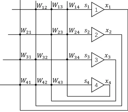
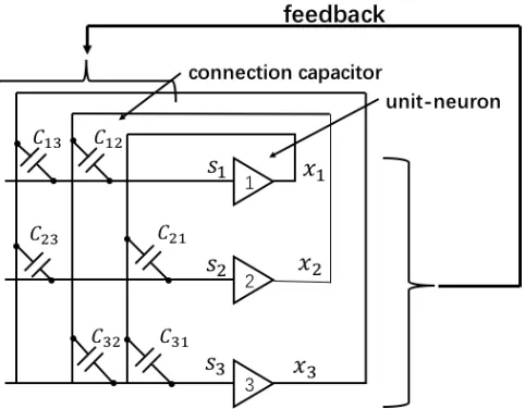
The Boltzmann machine consists of many unit neurons that are interconnected within a network. The
configuration of the network is shown in Fig 2.1. The output of each neuron feeds back into inputs of other neurons,
and each neuron exchanges signals with others to update its own output. The connection weights WQ] can be given
any desired value under the restrictions that WQ] = W]Q. In this network, each neuron i takes a weighted sum of the
inputs of the other neurons and the threshold connection weight according to the following equation
SQ= ]_QWQ]xQ (2.1)
where WQ] is the connection weight to neuron j to neuron i, and WQ] can be desired by the connection of each unit
neuron.
7
f sQ = 1/(exp (sQ/c)) (2.2)
where c is a control parameter which decreases slowly from a large positive value to zero during the
simulated-annealing process. Through this process, the Boltzmann machine network will not be stable until its state reaches the
minimum energy, ‘energy’ function defined by
−"A Q ]WQ]xQx] (2.3)
The minimum energy depends on the connections weight WQ], and WQ] is determined by the connections among
different inputs into the neuron networks. Detailed explanations will be given in the following chapters.
Fig. 2.1 Generic configuration of the Boltzmann machine with 4 unit neurons.
2.2.2 Circuit of the unit neuron
The single-electron has a number of nodes that are interconnected by the tunnel junctions. Electrons in each
node can tunnel to another node through the tunnel junction. This stochastic phenomenon can be utilized to design a
Boltzmann machine.
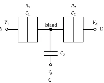
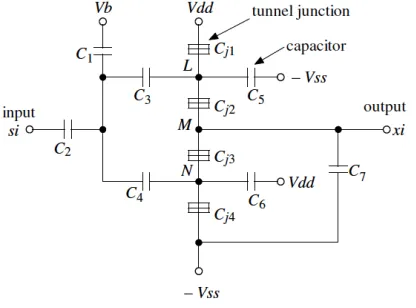
Fig 2.2 shows a unit-neuron circuit using single-electron devices. It consists of 4 tunnel junctions (C]" through
C]8) and 7 capacitors (C"through Cc), and is supplied with two bias voltages (i.e., VUU and −VRR ). The offset
voltage Vd is used to adjust the operating point of the circuit. Here, a set of {VUU, −VRR,Vd} is called the
control-parameter set. The output xQ of the circuit randomly alternates between 1 and -1, depending upon the probabilistic
fluctuations during the tunneling events. The circuit accepts an input voltage sQ and produces the corresponding
8
negative or zero value of sQ while the state of a positive output (i.e., ‘1’) is dominant for a positive value of sQ. The
other intermediate states may also be generated, but their duration is very short [5]. One can regulate the
control-parameter set to control the probability of an output ‘1’.
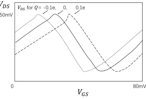
To create the stochastic neuron operation, we firstly try a lot of parameter sets for this unit neuron and plot their
stability diagram, as shown in Fig 2.3 (The stability diagram illustrates the internal states of a single-electron circuit
in a multi-dimensional space circuit variables) [6]. An example set of the capacitance parameter is
C]"= C]8= 1aF, C]A= C]7= 2aF,
C"= CA= 12aF, C7= C8= 4aF,
Ci= Cj= 10aF, Cc= 24aF,
We simulate the unit-neuron circuit on an operating line illustrated by PQ in figures 3.3 (a) through to (d). It can
be expected that the probability for generation of an output 1 can be changed from 1 to 0 continuously by increasing
input sQ to move the operating point from the H(0, −1, 0) region to the L(0, 0, 0) region on the line PQ. Additionally,
we will be able to change the control parameter for the probability function by regulating bias voltages VUU and
−VRR to change the width of the unstable region [7]. The parameters used here are the same as those given in Chapter
4, with tunnel resistances of 100k for tunnel junctions C]" and C]8, and 5M for C]A and C]7.
9
(a) (b)
(c) (d)
Fig. 2.3 An example of probability for generation of an output 1
2.2.3 Designing of the Boltzmann machine
By combining the above unit-neuron circuits into a neural network, a SET-based Boltzmann machine network
can be constructed, as shown in Fig 2.4. With a proper setting 𝑊lm, the network can eventually reach the lowest energy
state. Once the weights among neurons are set, the coupling capacitors 𝐶lm is given by
𝑊lm = opq
opqrop
10
11
Chapter 3
Self-Regulated ADC with Boltzmann Machine Network
3.1 The current study of ADCs
Analog and digital signal conversion (ADC) is necessary in modern signal processing systems. The development
of the semiconductor large-scale integrated (LSI) circuits promotes the ADC to develop in the direction of high
integration density, high speed, and low power dissipation. The ADCs based on the single-electron transistor (SET)
have the potential advantages of high integration density, low power dissipation, and high speed [8]. While intrinsic
background charges within SETs represent a big obstacle for many applications such as ADCs, a self-regulation
mechanism can be generally used to improve the immunity of SET-based circuits against these charges.
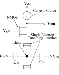
In many studies, the ADCs are designed with regarding the background charge as a constant. Fig 3.1 shows an
example of one hybrid ADC unit circuit design. The ADC unit circuit consists of an SET, an enhancement-type
NMOS transistor, and a current source. The discrete input analog signal is applied to the input gate IN of SET. The
drain–source current of SET depends on the input voltage and exhibits the periodic oscillation output characteristic
for a linearly increasing input signal. The gate of the NMOS transistor is biased by a gate voltage to keep the drain
voltage of SET constant approximately. However, in fact, the background charge changes all the time, so the constant
phase control cannot meet this requirement [8].
12
3.2 Improved ADC based on Boltzmann machine
Based on the idea of Boltzmann machine, we can consider the ADC into a neuron network to realize an operation
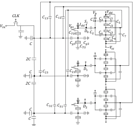
of self-regulation. As an example, Fig 3.2 shows a modified 3-bit ADC, where 𝐷s, 𝐷" and 𝐷A represent the three
digital outputs. Within a clock cycle, both 𝑉uu and −𝑉vv are decreasing slowly to realize a simulated-annealing
process, during which each output regulates the generation of other two with a feedback and reaches the most stable
state for a correct result [9].
The analog input signal 𝑉lwis inputted to the sampling and holding circuit first and then is divided by the signal
divider into n signals whose amplitudes are weighted by the ratio factors of 1/2l (𝑖 = 0, 1, ⋯ , 𝑛 − 1). Finally, the
analog signals are converted into the n-bit digital signal by the ADC circuit units. The sampling and holding circuit
block consists of a MOS switch transistor and a capacitor. The signal divider block consists of a capacitor net, which
produces discrete analog signals with weight coefficients 1/2l.
Fig. 3.2 Proposed 3-bit ADC with Boltzmann machine network
3.3 Simulation results of the proposed ADC structure
Both original and proposed ADCs were simulated by Cadence tools using the MIB model for SET devices. The
background charges are defined in the Verilog-A by using a random generator, which creates a noise waveform with
frequency of 10MHz and amplitude of no more than ±7% of the output. The length-width ratio of NNOS is
13
on its gate is 460mV. Therefore, the NMOS works under subthreshold condition. The parameters for the original
ADC are:𝑓}~• = 1MHz, the array capacitance 𝐶 = 5𝑓𝐹, 𝐶‚ƒ = 𝐶‚„ = 0.16𝑎𝐹, 𝐶†"= 0.32𝑎𝐹, 𝑅‚ƒ= 𝑅‚„ = 1𝑀Ω,
so that, inner one cycle, the duty cycle is 50%. And bias current 𝐼uu = 30𝑛𝐴. In a clock cycle, the 𝑉uu is
decreasing linearly from 3mV to zero by 300 steps, while −𝑉vvis increasing from -2mV to zero by 300 steps. Here,
the number of steps just represents how many sampling points we will use within the simulated-annealing time. The
larger number of steps we set, the slower the voltage decreases. Because in the Cadence simulator phenomenon, the
simulator just samples very few points from initial voltage to ultimate voltage if using the DC voltage source. We
can only reply on setting the voltage as the temperature to be deceased ladder to simulate a slowly-decreased process.
If the steps are less, which indicates the time of simulated-annealing process is short, the output will not have enough
time to be stable. Fig 3.3 gives out a comparison of simulated-annealing process with different steps. The connection
weights 𝑊lm is determined by the relations among each unit. Here, from the lowest bit to the highest bit, their input
voltages are decreased by 2 times. And the cycles of waveforms from lowest to highest are delay by 2 times. So:
𝑊"A= 𝑊A"= −2, 𝑊"7= 𝑊7"= −4, 𝑊A7= 𝑊7A= −2. The coupling capacitances are determined by using
equation as: 𝐶"A=0.34aF, 𝐶A"=0.27aF, 𝐶"7=0.17aF, 𝐶7"=0.3aF, 𝐶A7=0.17aF, and 𝐶7A=0.3aF. The parameter for
the unit-neuron circuit are given in Chapter 3.
Fig 3.4 shows our simulation results for the original 3-bit SET-MOS hybrid ADC without Boltzmann machine
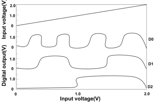
introduced, where the digit output may be incorrect with background charges. For instance, the analog voltage of
0.25V should be converted to 𝐷A 𝐷" 𝐷s= ‘001’, but ends up with ‘011’ instead due to the background charges. This
problem can be solved by the proposed ADC of Fig 3.2 with the process of simulated annealing. For instance, Fig
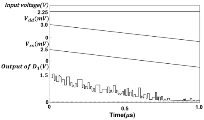
3.5 shows such a process for the output 𝐷", which converges to a correct voltage level with the control parameters
of 𝑉uu and −𝑉vv lowly decreasing. Simulation results from the proposed ADC structure are shown in Fig 3.6. with
14
Fig. 3.3 Simulated-annealing process by different simulation steps
Fig. 3.4 Simulation results for original 3-bit SET-MOS hybrid ADC without Boltzmann machine.
15
Fig. 3.6 Simulation results of proposed 3-bit ADC
3.4 Resolution Enhancement
In order to make the proposed hybrid ADC with Boltzmann machine operate properly, the circuit parameters
must satisfy the following condition:
𝐸}≫ 𝐾•𝑇 (3.1)
where 𝐸}is the charging energy, 𝐾•is the Boltzmann constant, and 𝑇 is the temperature. The charging energy 𝐸}
is given by
ED = H
I
AJ∑ (3.2) where 𝐶∑is the total gate capacitance of the SET transistor, and 𝑒 is the electron charge.
When T = 300K in particular, the maximum value of 𝐶∑is far below several aF, and this leads to the resolution
of no more than 4 bits for the input voltage swing of 2V. In order to obtain a higher resolution while keeping a
relatively-small value of 𝐶∑ (for room-temperature operation), an improved structure is proposed, as shown in Fig
3.7, where an amplifier is used to increase the input voltage swing by 2“ times (i.e., the resolution increases by M).
Here, M = 2 and the analog input voltage swing extends from 2V to 8V. The new input 𝑉QTA is converted into 5-bit
digital outputs, as opposed to 3-bit in Fig 3.2. Fig 3.8 shows simulation results of Fig 3.7 with digital output.
Compared with the two-step flash SET/MOS hybrid ADC circuit, our structure is much simpler and, more
16
Fig. 3.7 An improved 5-bit ADC with amplifier
Fig. 3.8 Simulation results of proposed 5-bit ADC
(a) (b)
17
3.5 Error Analysis
As the resolution keeps increasing with M, two main errors may occur. First, the high resolution introduces
more feedback branches and capacitances, which contribute more charges 𝑄 on SET’s island as 𝑄 = 𝐶∑∙ 𝑉 . The
output 𝑥l from the unit-neuron circuit is around − 5m~5mV. For a 5-bADC circuit, 𝑄 is around 1×10⁶As𝐶, which
means there is an equivalent of 0.0625e added to the island to shift the phase of the output voltage. As 𝐶∑increases,
there could be a large phase shift. However, the maximum error is 1LSB as long as the phase shift is less than 180°.
Fig 3.10 illustrates a comparison of the output oscillations with and without a phase shift. For example, in this figure,
the input voltage of 0.25V should be converted into 00001, but it ends up with00010 incorrectly due to the phase
shift. The second possible error comes from the amplifier. For instance, if the amplifier has an error of ±𝛼%, the
improved ADC can just ensure the accuracy with 𝑁š›œbits for a maximum error of 1 LSB, where 1/2•žŸ > 𝛼% >
1/2•žŸ r". Fig 3.11 shows the simulation results of Fig 3.6 with 𝛼% = 10%. It can be seen from the figure that the
least significant bits 𝐷s and 𝐷" are very sensitive to the error especially for a large input, while the most significant
bits 𝐷A, 𝐷7and 𝐷8are less affected by the error. This indicates that the amplifier error puts a certain limit on
further resolution enhancement. In summary, the high resolution with the improved ADC is subject to both low
capacitances and accurate amplifier.
18
19
Chapter 4
Improved full adder based on Boltzmann machine
4.1 Design of new full adder structure
Full adder is a key element for arithmetic and logic units. It is therefore of special interest to design the adders
with extremely n PTL (pass transistor logic), TLGs (threshold logic gates) and serial SETMOS architecture, they
suffer from either low temperature operation or low current drivability. Even if the circuits of full adder are improved
by using hybrid SET-CMOS devices, the background charge still influences the accuracy of any circuits including
SETs [10].
In 2003, H. Inokawa proposed a basic SET component with a constant-current load [11,12] in order to overcome
SET’s inherent disadvantages of low output resistance. A one-bit CMOS-like single-electron full adder was also
presented recently [13].
Therefore, we propose a completely new one-bit structure full adder. Firstly, according to the truth table of full
adder function, as shown in table 1, we can plot the waveforms of output for sum and carry, as shown in Fig 4.1.
where VA, VB and VC represent two input bits and a carry-in bit. It can be seen that when using Vin = 𝑉¡+ 𝑉•+ 𝑉o as
x-axis, the frequency of carry is 3 times lower than that of sum [14]. Similar with the idea of ADC, we build a network
to produce the curves shown in Fig 4.2 to simplify the full adder design. We produce 2 discrete input signals 𝑉lw
with weight coefficients 1/3l, 𝑖=0, 1. The full adder unit circuit consists of an SET, an enhancement-type NMOS
transistor, and a current source, as shown in Fig 4.2. In order to make the three inputs have same effort on islands,
these inputs will go through the same capacitance array. And the capacitors ‘1C’ and ‘1/3C’ is designed to produce
the proper sum and carry curves. The V¢, V&and VJ generates voltage ‘0’ or ‘1’ separately, and the signals are sent to
the SET block. The outputs from SET then are sent to neuron network. Inner this network, the minimum energy is
based on that the ratio of cycles between the waveforms of sum and carry is 1:3. Following this rule, if the total
charges of the island changed by the background charge, the disordered signals from the SET can be amended within
20
TABLE 1 Truth table of full adder
A B C 𝑉lw = (𝐴 + 𝐵 + 𝐶) Sum Carry
000 0 0 0
001 1 1 0
010 1 1 0
100 1 1 0
011 2 0 1
101 2 0 1
110 2 0 1
111 3 1 1
Fig. 4.1 Expected waveforms of sum and carry
21
4.2 Simulation results and analysis
The hybrid full adder was simulated by Cadence tools using the MIB model for SET devices. The background
charges are defined in the Verilog-A by using a random generator, which creates a noise waveform with frequency
of 10MHz and amplitude of no more than ±7% of the output. The length-width ratio of NNOS is 300nm/180nm, the
threshold voltage of this kind of NMOS transistor is around 480 mV. The biased voltage applied on its gate is 460mV.
Therefore, the NMOS works under subthreshold condition.
At 300K, the simulation results are shown in Fig 4.3. The full adder can work normally at room temperature,
although the output signals are not with full swings. Because the inhere disadvantages of SET, there may occur a
wrong sum or carry or both sometime. For example, the input 𝑉¡, 𝑉•and 𝑉o are 1, 1 and 0, separately, then sum
should be 0 and carry should be 1. However, because the background charge comes into the island, which cause the
total charge of the island changes, so the output from the sum is wrong.
All parameters of the Boltzmann-machine-based hybrid SETMOS full adder for our simulation are chosen as
follows: one cycle=1𝜇𝑠, the array capacitance 𝐶 = 5𝑓𝐹, 𝐶‚ƒ = 𝐶‚„ = 0.16𝑎𝐹, 𝐶†"= 0.32𝑎𝐹, 𝑅‚ƒ= 𝑅‚„ = 1𝑀Ω,
so that, inner one cycle, the duty cycle is 50%. And bias current 𝐼uu = 30𝑛𝐴. In a clock cycle, the 𝑉uu is
decreasing linearly from 3mV to zero by 250 steps, while −𝑉vvis increasing from -2mV to zero by 250 steps. The
connection weights 𝑊v} is from the neuron sum to neuron carry, and 𝑊}v is from neuron carry to neuron sum. They
are determined by the relations between carry and sum. Here, from the lowest bit to the highest bit, their input voltages
are decreased by 3 times. And the cycles of waveforms from lowest to highest are delay by 3 times. According to
equations, we set WRD= −0.25, WDR= −0.75, and the coupling capacitances can be set as follows: CRD= 0.16aF and CDR= 0.48aF.
The parameter for the unit-neuron circuit are given in Chapter 2.
By applying Boltzmann machine network on this full adder structure, we can realize the function of
self-regulated to fix the wrong bit. When we change x-axis from ‘Time’ to the calculation of sum of 𝑉¡, 𝑉•and 𝑉o, then
input them as per the sequence of truth table, we can clearly find that the sum and carry are following the relations
22
Furthermore, a multi-bit full adder can be constructed by cascading several full adder cells in series, as shown
in Fig 4.5. This structure is called a ripple-carry adder. 𝐶s is 0 at the beginning, and from 𝐶", is generated from the
upper level. The Boltzmann machine is only utilized inner one-bit as feedback.
However, for a multi-bit full adder, there may be another error. Because the SET oscillates as a sine wave, so the
output may not be a standard square wave. Therefore, the propagation delay of such a structure is determined by the
critical path. The delay of a n-bit adder is approximated by:
𝑡›uu¨©≈ 𝑛 − 1 𝑡}›©©ª+ 𝑡v«š (4.1)
or
𝑡›uu¨©≈ 𝑛𝑡}›©©ª (4.2)
where 𝑡}›©©ª" is the delay of each bit from VJ¬ to VJ-. And 𝑡v«š is the delay of last bit from VJ-®¯ to VJ-. The
propagation delay is measured between the 50% transition points of the input and output waveforms. From the
simulation results in Fig 4.6, 𝑡v«š is equal to 1.65ns, and 𝑡}›©©ª is 1.3ns. Therefore, the total time delay is determined
by equation (4.1). As an example, a two-bit ripple-carry adder is around 2.95ns. Although the delay time may be a
little longer than that implemented by pure MOSFET circuit, the hybrid SETMOS full adder consumes much less
area which can be accepted to a certain extent.
23
(a) (b)
Fig. 4.4 Output for sum and carry with different x-axis
(a) Time (b) Sum of 𝑉¡, 𝑉•and 𝑉o
Fig. 4.5 An example of 2-bit ripple carry adder
(a)
(b)
24
Chapter 5
Conclusion
In order to eliminate the error of the SET-based circuits caused by the background charge, we introduce the
neuron network to hybrid circuits, with increased time redundancy. The single-electron circuit has a stochastic nature
of operation because the waiting time for electron tunneling shows probabilistic fluctuation. Therefore, the operation
of the Boltzmann machine can be easily implemented using such a single-electron circuit that modulates its output in
response to the fluctuation in the tunnel waiting time. We utilized a single-electron neuron circuit that can produce
the function required for the Boltzmann machine neuron; the proposed neuron circuit. Firstly, a modified ADC with
Boltzmann machine network has been presented. The results show that the immunity of the ADC against background
charges is significantly improved. The resolution enhancement as well as error analysis with the ADC have also been
discussed and simulated. Secondly, representative hybrid SETMOS logic circuits are developed to avoid the
disadvantage. We rebuilt a one-bit full adder based on Boltzmann machine. Simulation result shows that hybrid
SETMOS full adder can work normally at room temperature. The proposed one-bit full adder requires much less area
than its CMOS counterpart while maintaining the high performance.
And we also proposed a possible way to build a multi-bit full adder. It is expected that our idea can be extended
25
References
[1] J. A. Hutchby, G. I. Bourianoff, V.V. Zhirnov, and J. E. Brewer, "Extending the road beyond CMOS,"
IEEE Circuits Devices Mag., vol.18, pp. 28–41, Feb. 2002.
[2]S. M. Goodnick and J. Bird, “Quantum-effect and single-electron devices,” IEEE Trans. on
Nanotechnology, vol. 2, no. 4, December 2003, pp. 368-385
[3] M.T.Bohr, “Nanotechnology goals and challenges for electronic applications,” IEEE Trans. on
Nanotechnology, vol.1, no.1m March 2002, pp.56-62.
[4] T. Yamada, M. Akazawa, T. Asai and Y. Amemiya, “Boltzmann machine neural network devices using
single-electron tunnelling,” IEEE Trans. on Nanotechnology, vol. 12, no. 1, pp. 60-67, Dec. 2001.
[5] M. Akazaw and Y. Amemiya, “Boltzmann machine neuron circuit using single-electron tunneling,”
Appl. Phys. Lett. 70670–2, 1997.
[6] E. Aarts and J. Korst. Simulated Annealing and Boltzmann Machines—A Stochastic Approach to
Combinatorial Optimization and Neural Computing. 1989, New York: Wiley.
[7] G. E. Hinton and T. J. Sejnowski. Learning and Relearning in Boltzmann Machines Parallel Distributed
Processing—Explorations in the Microstructure of Cognition. 1986, vol 1, ed. D. E. Rumelhart, J. L.
McClellend and the PDP Research Group, Cambridge, MA: MIT Press, pp. 282–317.
[8] X. Ou and N. Wu, “Analog-digital and digital-analog converters using single-electron and MOS
transistors,” IEEE Trans. On Nanotechnology, vol. 4, no. 6, pp. 722-729, Nov. 2005.
[9] M. Goossens. Analog Neural Networks in Single-Electron Tunneling Technology. 1998, Delft, the
Netherlands, Delft University Press.
[10] F.Capasso and R.Kiehl, “Resonant tunneling transistor with quantum well base and high-energy
injection: A new negative differential resistance device,” J. Appl. Phys., vol. 58, p. 1366, 1985.
[11]
H. Inokawa and Y. Takahashi, “Experimental and simulation studies of single electron-transistor-based
multiple-valued logic,” Proceedings of 33rd International Symposium on Multiple-Valued Logic (ISMVL),
26
[12] H. Inokawa, A. Fujiwara, and Y. Takahashi, “A multiple-valued logic and memory with combined
single-electron and metal-oxide-semiconductor transistors,” IEEE Transactions on Electron Devices, vol.
50, no. 2, pp. 462–470, 2003.
[13] D. Griveau, S. Ecoffey, R. M. Parekh, M. A. Bounouar, F. Calmon, J. Beauvais and D. Drouin,
“Single-electron CMOS-like one bit full adder,” Proceedings of 13th International Conference on Ultimate
Integration on Silicon (ULIS), March. 2012.
[14] Bingcai Sui, Liang Fang and Yaqing Chi, “Full adder designed with MOSFET and single-electron
transistor hybrid circuit,” Proceedings of Asia Pacific Conference on Postgraduate Research in
27
Permission to Use Previously Published/Submitted Papers
Dr. Chunhong Chen gives permission to Zihan Zhang to include the following papers into her Master’s thesis.
1) Paper accepted in poster session for — Proceedings of 2017 IEEE International Conference on Nanotechnology
(IEEE-Nano’17), July 2017, Pittsburgh, PA, USA
Entitled:
Zihan Zhang and C. Chen, “Improving the immunity of hybrid SET/MOS circuits using Boltzmann machine network,”
in Proceedings of the IEEE International Conference on Nanotechnology, July 2017, pp. 233-236.
2) Paper to be submitted for publication
Entitled:
Zihan Zhang and C. Chen, “A hybrid SET/MOS full adder with improved immunity against noises based on
Boltzmann machine network”
Sincerely,
28
Vita Auctoris
Zihan Zhang was born in 1993 in Zhengzhou, China. She completed her Bachelors of Science degree from the
South-central University for Nationalities in 2011. Her research interests include single-eletron technology and Boltzmann
machine network. She is currently a candidate for the Master’s degree in Electrical and Computer Engineering at the