ABSTRACT
LEE, MENG-CHIA. Developing Physics-based Models for 4H-SiC High Voltage Power Switches – MOSFET, IGBT and GTO. (Under the direction of Dr. Alex Huang.)
The goal of this dissertation is to develop physics-based equivalent circuit models for
15kV~20kV 4H-SiC power switches. The previous modeling works will be reviewed, and the
parameter extraction methodologies will be discussed.
MOSFET is modeled using a voltage-controlled current source for channel current and
three nonlinear capacitances for the transient behavior. The high electron saturation velocity
and its effect on the saturation current level will also be discussed. Final model has been
implemented in Simulink/Matlab, and the execution time for the turn-on and off transient is
less than 1 second.
IGBT Analytical model that translate the local excess carrier to the diffusion
capacitance will be derived first and implemented in a sub-circuit manner into
Simulink/Matlab. A novel parameter extraction technique – Excess carrier density mapping
(ECDM) – using inductive switching waveforms is introduced. The execution time of the
model is about 7 seconds and and 2 seconds for a turn-off and turn-on transient, respectively.
IGBTs with two-zone drift region for slowing down the turn-off dv/dt are also proposed based
on the developed analytical model.
Finally, 4H-SiC p-GTO model based on the IGBT one is developed. Region-wise
lifetimes throughout the drift region was observed when using the proposed ECDM technique.
Simulated waveforms using region-wise lifetime have shown better fitting results than the case
using constant lifetime. The difference between n-type and p-type ambipolar switches will be
© Copyright 2015 Meng-Chia Lee
Developing Physics-based Models for 4H-SiC High Voltage Power Switches – MOSFET, IGBT and GTO
by Meng-Chia Lee
A dissertation submitted to the Graduate Faculty of North Carolina State University
in partial fulfillment of the requirements for the degree of
Doctor of Philosophy
Electrical Engineering
Raleigh, North Carolina 2015
APPROVED BY:
________________________________ ________________________________ Dr. Alex Q. Huang Dr. B. J. Baliga
Chair of Advisory Committee
ii DEDICATION
To my parents,
iii BIOGRAPHY
Lee, Meng-Chia was born in Yunlin, Taiwan. He received his MS degree in Electronic
Engineering from National Tsing Hua University (HsinChu, Taiwan) in 2009. His research
focus was lateral 4H-SiC transistors on semi-insulating substrate. In 2010, he enrolled in
graduate school at North Carolina State University (Raleigh, NC) for pursuing his PhD degree
in Electrical Engineering under the guidance of Dr. Alex Q. Huang. His field of interests
iv ACKNOWLEDGMENTS
An email from my advisor, Dr. Alex Q. Huang, five years ago had unfolded a new chapter
of my academic career here in the USA. I would like to express my sincerest appreciation for
his second to none guidance throughout the course of my PhD, shaping my professional
characteristics, polishing my logical thinking in the research, inspiring me with his abundant
ideas and years of experience, and above all, providing an academic latitude for me to
maximize my potential to where I could ever imagine.
I would like to thank Dr. B. J. Baliga for being my committee. His pioneer role in the field
of power semiconductor devices with his enlightening lectures offered at NCSU have
motivated me to advance in the academic world. The solid and systematic analytical skills
taught in the class have greatly influenced me later in my research. His valuable inputs on my
dissertation further strengthen the claims and the statements made in this work.
I would like to thank my committee member Dr. Woongje Sung for his mentoring and
suggestions for my research topics. His precise and organized manner toward research have
great influences on my oral and written presentation skills. His great patience also encouraged
me to discuss any problems I have during my PhD life.
I would also like to thank Dr. Chih-Hao Chang in the Mechanical Engineering Department
for being in my committee. I thank my senior, Xing Huang and Edward Van Brunt for
discussing lots of technical questions in the fab and the simulation tools. I thank Xiaoqing for
supporting my research with his knowledgeable characterization skills. I thank Ankan De for
teaching me how to implement my equations into the Matlab, spending time with me during
the weekend in the initial phase of my modeling work. Finally, I would like to thank my parents
v TABLE OF CONTENTS
List of Tables………...………...iiiv
List of Figures………...………....ix
Chapter 1 Introduction ... 1
1.1 Recent progress on high voltage 4H-SiC power switches ... 1
1.2 Frequency capability V.S. Device Size (15kV MOSFET and IGBT) ... 4
1.3 Challenge and Outlook for SiC IGBTs for high frequency operation ... 7
1.4 The Purpose of this Modeling Work ... 9
1.5 Outline of this work ... 10
Chapter 2 10A 15kV 4H-SiC MOSFET Modeling ... 12
2.1 Review of existing models ... 13
2.2 On-state modeling of the proposed model ... 16
2.2.1 Drift region resistance ... 16
2.2.2 Velocity saturation in the drift region ... 18
2.2.3 MOSFET current equation and its parameters ... 21
2.3 Dynamic switching modeling ... 27
2.3.1 Switching dynamics during turn-on ... 27
2.3.1 Switching dynamics during turn-off ... 30
2.3.2 Extraction of parasitic capacitance ... 32
2.4 Model implemented in Simulink/Matlab ... 35
2.5 Model validation ... 38
Chapter 3 20A 15kV 4H-SiC n-IGBT Modeling... 43
3.1 Review of IGBT model ... 43
3.1.1 Hefner’s model (E.D.C) ... 44
3.1.2 Lumped charge model (E. L. C.): ... 48
3.1.3 Fourier-series-based model: ... 49
3.2 IGBT theory and principle ... 52
3.2.1 Ambipolar diffusion equation at arbitrary injection level ... 53
3.2. 2 Analytical expression of on-state voltage drop along the drift region ... 54
3.2.3 Injection efficiency as a function of total current density... 55
3.2.4 Common emitter current gain 𝛽 ... 58
3.2.5 Dynamic carrier density in the depletion region ... 58
vi
3.3.1 Charge continuity equation (CCE) ... 62
3.3.2 Generate the carrier density profile ... 64
3.3.3 Tracking the local carrier information ... 65
3.3.4 KCL ... 66
3.3.5 KVL ... 70
3.4 IGBT model implementation in Simulink/Saber ... 71
3.4.1 Connect the components using the derived KCL ... 71
3.4.2 CCE ... 72
3.4.3 The Voltage-dependent capacitances ... 73
3.4.4 The drift region resistance ... 74
3.5 Parameter extraction procedure ... 74
3.5.1 Excess carrier distribution mapping ... 76
3.5.2 Extract 𝑁𝐷 and 𝑣𝑠𝑎𝑡, 𝑝 ... 77
3.5.3 Extract 𝜏𝐷 and ℎ𝑛 ... 79
3.5.4 Extract 𝑑2/𝜏𝐵′ and 𝑄𝐻 ... 81
3.5.5 Extract d ... 83
3.5.6 Extract parameters related to MOS channel ... 84
3.6 Model Validation ... 87
3.6.1 On-state IV... 87
3.6.2 Transient modeling ... 90
3.6.3 Charge dynamic during the switching ... 94
3.7 Comparison between Hefner’s model and the proposed model ... 99
3.7.1 Difference I – Charge Continuity Equation ... 99
3.7.2 Difference II – Charge Continuity Equation ... 101
3.7.3 Difference III – Collector current ... 102
3.7.4 Difference IV – Ambipolar parameter extraction ... 104
3.8 Computational speed ... 107
Chapter 4 Novel Structure for High Voltage 4H-SiC IGBT ... 109
4.1 Review of 4H-SiC IGBT optimization works ... 110
4.1.1 Optimum carrier density profile ... 110
4.1.2 Current enhancement layer ... 111
4.1.3 Buffer layer optimization ... 112
4.1.4 Drift region optimization avoiding high dv/dt ... 113
vii
Chapter 5 4H-SiC p-GTO ... 120
5.1 Introduction of 4H-SiC p-GTO ... 120
5.2 N-type and p-type ambipolar transistors ... 122
5.2.1 Injection capability between n-type and p-type devices ... 122
5.2.2 Turn-off speed between n-type and p-type devices ... 125
5.3 Developing sub-circuit p-GTO model ... 127
5.4 Parameter Extractions and model validation ... 130
5.4.1 Evaluate the accuracy of the ECDM near the upper base region ... 131
5.4.2 Effective high level lifetime 𝜏𝐷, 𝑒𝑓𝑓 and ℎ𝑝 ... 135
5.4.3 𝑑2/𝜏𝐵′ , QH and d ... 137
5.4.4 Effective N-base lifetime ... 139
5.5 Model Validation ... 140
5.5.1 Steady-state IV curve ... 140
5.5.2 Switching Transient validation ... 141
Chapter 6 Summary ... 144
viii LIST OF TABLES
Table 1.1 Power loss estimation empirical models for MOSFET and IGBT ... 4
Table 2.1 Resistance calculated using different methods. ... 17
Table 2.2 MOSFET current equations for steady-state ... 21
Table 3.1 Ambioplar model categories ... 43
Table 3.2 Summarized equations used in the proposed model. ... 85
Table 3.3 Extracted parameter inputs of the proposed model at different temperatures. ... 86
Table 4.1 Combinations of the parameters in the two-zone dirft region. ... 117
ix LIST OF FIGURES
Figure 1-1 Simplied cross-section of MOSFET, IGBT and GTO. ... 1
Figure 1-2 IV curves at different temperatures for 15kV 4H-SiC MOSFET, n-IGBT and p-GTO. ... 2
Figure 1-3 Recent progress on 4H-SiC high-voltage ambipolar switches. ... 2
Figure 1-4 Frequency capability V.S. device size for 15kV MOSFET and IGBT at different power rating. ... 6
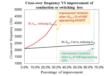
Figure 1-5 Crossover frequency V.S. Improvements in switching or conduction loss. ... 7
Figure 2-1 The flow chart of parameter extraction of the proposed 4H-SiV 15kV MOSFET. ... 12
Figure 2-2 Simulated IV curves of 4H-SiC 650 V MOSFET with constant channel mobility ... 14
Figure 2-3 Simulated IV curves of 4H-SiC 15 kV MOSFET (overlapped with 650 V) with constant channel mobility. ... 15
Figure 2-4 Simplified Cross-section and simple equivalent circuit of 4H-SiC 15kV MOSFET. ... 16
Figure 2-5 Device dimension and resistance estimation of 10A 4H-SiC 15kV MOSFET. ... 17
Figure 2-6 The illustration of the difference between E field in low and high doping drift region .... 18
Figure 2-7 Electron velocity plots of SiC MOSFET with ND=4.5E14 cm-3 at Vg=15 volts and Vdd= 45, 100, 150, 170 volts. Current start to saturate at Vdd=150 volts. ... 19
Figure 2-8 Electron velocity plots of SiC MOSFET with ND=4.5E14 cm-3 at Vg=15 volts and Vdd= 1, 4, 6, 7.5 volts. Current start to saturate at Vdd=4 volts. ... 19
Figure 2-9 Electron velocity V.S. electric field for 4H-SiC ... 20
Figure 2-10 Threshold voltage extraction at different temperatures. ... 22
Figure 2-11 Parameters optimization by iterating to find the minimum sum of least square root. ... 23
Figure 2-12 Simulated and measurement results for 15kV MODFET at lower bias. ... 23
Figure 2-13 Simulated and measurement IV curves of 15kV MOSFET at different temperatures. ... 24
Figure 2-14 Transconductance in the linear region and threshold voltage as a function of temperature. ... 24
Figure 2-15 Transconductance in saturation region and saturation current vs gate voltage ... 25
Figure 2-16 Modeled IV curves of 15kV MOSFET in linear, transition, and saturation region. ... 27
Figure 2-17 Turn-on transient and current flows. Solid and dashed lines are the conduction and displacement current, respectively. ... 28
Figure 2-18 Typical turn-on waveforms of a MOSFET with a freewheeling diode. ... 28
Figure 2-19 Turn-on transient and current flows. Solid and dashed lines are the conduction and displacement current, respectively. ... 30
Figure 2-20 Typical turn-on waveforms of a MOSFET with a freewheeling diode ... 30
Figure 2-21 The measured output capacitance of the 15kV MOSFETs compared to calculated values. ... 33
Figure 2-22 Typical CV curve for the input capacitance of a MOSFET. ... 34
Figure 2-23 Extracted Coss, Ciss and Crss for the 15kV MOSFET. ... 34
Figure 2-24 Non-linear capacitance implementation in Simulink/Matlab. Measured C-V curve can be put into the look up table. ... 35
Figure 2-25 A 15kV MOSFET model in Simulink/Matlab. ... 36
Figure 2-26 Inductive load switching of the 15kV MOSFET with a simplified Schottky diode model. ... 37
x Figure 2-28 Simulated and measured turn-on waveforms of the 15kV MOSFET for different gate
resistance. ... 39
Figure 2-29 The actual turn-on loss is 25% percent higher than the measured loss. VDD= 6kV. ... 40
Figure 2-30 Energy loss versus current prediction at 25oC. VDD=9kV. ... 41
Figure 2-31 Energy loss versus current prediction at 125oC. VDD=9kV. ... 41
Figure 2-32 Total switching loss at 25 and 125oC. VDD=9kV. ... 42
Figure 3-1 Equivalent circuit in Hefner’s model. ... 44
Figure 3-2 Illustration of the redistribution current induced carrier density profile. ... 45
Figure 3-3 Illustration of the carrier dynamics in a lumped charge model. ... 48
Figure 3-4 The Fourier-series-based solution for carrier density profile and its algorithm. ... 50
Figure 3-5 Device physics during on-state that will be discussed in the section. ... 52
Figure 3-6 Device physics during switching transient that will be discussed in the section. ... 52
Figure 3-7 Illustration of the sudden current drop after the IGBT gate turnoff... 57
Figure 3-8 Hole carrier densities before punch-through during turn-off. ... 60
Figure 3-9 The slice of charge marked by the dashed line and the expression of its change rate. ... 61
Figure 3-10 Figurative steps of the proposed IGBT model. ... 62
Figure 3-11 Simulated snapshots of carrier density distribution during the inductive turn-off of 4H-SiC IGBT. ... 64
Figure 3-12 The simplified equivalent circuit (left) and the proposed equivalent circuit (right) based on derived KCL. ... 68
Figure 3-13 Detailed illustration of the current components going in and coming out of the transition region. ... 69
Figure 3-14 Proposed IGBT model implemented in Simulink/Matlab. ... 71
Figure 3-15 Charge continuity equation block in Simulink/Matlab for dyanmic charge calculation. 72 Figure 3-16 The implementaion of non-linear capacitance in Simulink/Matlab. ... 73
Figure 3-17 The drift region voltage drop calculator in Simulink/Matlab. ... 74
Figure 3-18 Proposed parameter extraction procedure for 4H-SiC IGBT. There are five steps and requires only two experiments... 75
Figure 3-19 Validation of proposed direct mapping technique using simulation... 77
Figure 3-20 Dynamic carrier and the effective saturation velocity. The background doping ND can be obtained by extrapolating the curve to current=0. ... 79
Figure 3-21 The result of direct mapping of carrier density profiles at different temperatures for the 10A 4H-SiC n-IGBT. Dashed line: extracted. Solid line: fitting using exponantail expression (𝐴 ∙ 𝐸𝑥𝑝𝑋𝐿 + 𝐵 ∙ 𝐸𝑥𝑝(−𝑥𝐿)). ... 80
Figure 3-22 Extracted ambipolar lifetime and ℎ𝑛. ... 80
Figure 3-23 Extracted constant of 𝑑2𝜏𝐵′ at different temperature. ... 83
Figure 3-24 Simulated turn-off waveforms for different buffer layer thickness at fixed 𝐶 ≡ 𝑑2𝜏𝐵′. ... 84
Figure 3-25 Modeled and measured IV curves of 15kV 4H-SiC at different temperatures. ... 87
Figure 3-26 The extracted threshold voltage and transconductance as a function of temperature. ... 88
Figure 3-27 The equivalent circuit model during the steady-state. ... 89
Figure 3-28 15kV IGBT modeled in an double pulse switching circuit in Simulink. ... 90
Figure 3-29 Simulated and measured turn-off waveforms at different current at 25oC. ... 91
Figure 3-30 Simulated and measured turn-off waveforms at different current at 125oC. ... 91
Figure 3-31 Measured 15kV 4H-SiC turn-off waveforms under different conditions. ... 92
Figure 3-32 Simulated 15kV 4H-SiC turn-on waveforms under different conditions. ... 92
xi
Figure 3-34 Simulated 15kV 4H-SiC turn-on waveforms under different conditions. ... 93
Figure 3-35 Instantaneous physical quantities during turn-off plotted in the Simulink. ... 94
Figure 3-36 Instantaneous physical quantities during turn-on plotted in the Simulink. ... 97
Figure 3-37 Energy loss during turn-off and turn-on at 25oC. VDD=9kV, Rg=10ohm. ... 98
Figure 3-38 Energy loss during turn-off and turn-on at 125oC. VDD=9kV, Rg=10ohm. ... 99
Figure 3-39 Side-by-side comparison of the charge continuity equation between Hefner’s and the proposed model. ... 100
Figure 3-40 Side-by-side comparison of the calculation of the drift region resistance between Hefner’s and the proposed model. ... 101
Figure 3-41 Side-by-side comparison of the diffusion capacitance between Hefner’s and the proposed model. ... 103
Figure 3-42 Difference between Hefner’s and the proposed model in terms of lifetime extraction methodology. ... 104
Figure 3-43 Hefner’s model compared with the measurement results. ... 105
Figure 3-44 Side by side comparison of voltage waveforms and normalized error bars for the proposed and Hefner’s model. ... 106
Figure 3-45 The proposed model compared with the measurement result. ... 106
Figure 3-46 Improving the computational speed by inserting the low pass filter. ... 107
Figure 3-47 The low pass filter in the Charge Continuity Equation (CCE) block. ... 108
Figure 4-1 IGBT optimizations and theories that will be discussed in this chapter. ... 109
Figure 4-2 Three different types of carrier density profile and their corresponding turn-off waveforms. ... 110
Figure 4-3 Turn-off loss and Vdrift V.S. increment of the boundary carrier densities. ... 111
Figure 4-4 Proposed two-zone IGBT. The electric field will be terminated before the maximum voltage rating. Higher doping in zone 2 will result in faster voltage ramping during turn-off. ... 114
Figure 4-5 Different electric fields of five combination of drift region parameters at 8kV. ... 117
Figure 4-6 Turn-off waveforms of different drift region designs. ... 118
Figure 4-7 𝐸𝑜𝑓𝑓 − 𝑉𝑐𝑒, 𝑠𝑎𝑡 trade-off curve for different designs of drift region. ... 119
Figure 5-1 Cross section of a 22kV 4H-SiC p-GTO. ... 120
Figure 5-2 Injection efficiency function of n- and p-IGBT that will result in the same stored charge at given current. ... 124
Figure 5-3 The inductive turn-off for n- and p-IGBT with the same amount of stored charge. ... 126
Figure 5-4 Equivalent circuit for p-GTO and n-IGBT. ... 127
Figure 5-5 4H-SiC p-GTO model implemented in Simulink/Matlab. ... 128
Figure 5-6 Proposed parameter extraction procedure for 4H-SiC GTO. There are six steps and only requires two experiments. ... 130
Figure 5-7 The inductive turn-off of two p-GTO with different injection efficiency are simulated in TCAD. Current density is 30A/cm2. ... 132
Figure 5-8 Extracted carrier density profile using the proposed ECDM technique. ... 132
Figure 5-9 Switching waveform zoom-in at low voltage range. ... 133
Figure 5-10 The depiction of the dynamic of excess carrier during turn-off. ... 134
Figure 5-11 A model describing the carrier dynamic during switching. A slice of local excess charge with a tilted rectangular shape is being removed at each time step. ... 135
Figure 5-12 The extracted carrier profile using ECDM technique and the fitted curve using different lifetime... 136
xii Figure 5-14 Simulated and measured IV curve for 15kV p-GTO at 25oC. ... 140 Figure 5-15 Measured versus simulated turn-off waveforms at different current level. The ambipolar lifetime of 2.2 𝜇𝑠 is used throughout the drift region. ... 141 Figure 5-16 Measured versus simulated turn-off waveforms at different current level. The ambipolar lifetime of 3.5 𝜇𝑠 is used near the surface and 1.5 𝜇𝑠 is used closed to the cathode... 142 Figure 5-17 The switching speed of 15kV n-IGBT is more than 10 times faster than p-GTO. ... 143 Figure 5-18 Improvement of the accuracy of the proposed model by incorporating two-zone
1
Chapter 1
Introduction
Introduction
1.1 Recent progress on high voltage 4H-SiC power switches
Figure 1-1 are the simplified cross-sections of >10kV 4H-SiC power switches that have
been developed over the past decade [1]. Figure 1-2 shows the measurement results of the IV
curves at 25oC and 125oC for 15kV device technologies. 4H-SiC GTO has the best conduction characteristics and is insensitive to the temperature, while the conductivity of MOSFET has
dropped more than 50% from 25oC to 125oC.
2 Figure 1-3 summarizes the recent >10kV 4H-SiC technologies of ambipolar transistors.
Figure 1-3 Recent progress on 4H-SiC high-voltage ambipolar switches.
3 From this trend shown in Figure 1-3, n-channel devices seem to be the focus for the future
IGBT device technologies. It also has been experimentally [2] and theoretically [3] that
n-channel IGBTs can switch faster than p-n-channel ones. The reason that n-GTO has not been
demonstrated might be due to the poor quality of P+ substrate [4].
4H-SiC MOSFETs are strong candidates for the application in solid-state transformer (SST)
for future smart grid technology because the faster switching speeds compared to 6.5 kV Si
IGBTs [5]. The major advantage is that the lower switching loss due to its unipolar nature
allows the device to operate at higher frequency, which significantly reduces the size of the
passive components.
4H-SiC IGBTs are gate-controlled devices with conductivity modulation during on-state
that can provide smaller conduction loss, and therefore, higher current capability than 4H-SiC
MOSFET for the same voltage rating. For distribution level SST with up to tens of kilo watts
(2.3~35kVA) [6], however, 15kV MOSFETs seems to be slightly favorable than its IGBT
counterparts due to the switching loss for MOSFET is about half of the value of IGBTs [7].
Nevertheless, current trend or preference may be upset by the ongoing improvement and
evolving on SiC device technologies. For example, a 16kV SiC injection enhanced n-IGBT
(IEGT) [8] and a 22kV SiC n-IGBT have just been introduced in 2014 [9]. At 20kV voltage
rating with junction temperature of 125oC, SiC MOSFET technology might suffer from a much higher conduction loss due to its unipolar nature.
For the applications of higher power rating (MVA~GVA) with lower frequency and high
current, e.g. FACT and HVDC, SiC GTOs are the ideal candidates for the enabling
4 density profile in a thyristor is similar to a P-i-N diode, providing superior on-state
characteristics than IGBTs.
1.2 Frequency capability V.S. Device Size (15kV MOSFET and IGBT)
It will be shown in this section that, for the current 15kV SiC device technologies,
MOSFETs seem to be more favorable than IGBTs in terms of frequency capability. Based on
the measurement results of 15kV devices at 125oC for switching loss (both turn-on and off) and conduction loss in [7], an empirical power loss estimation is provided in Table 1.1.
𝐏𝐜𝐨𝐧𝐝𝐮𝐜𝐭(𝑾) 𝐄𝐬𝐰,𝐬𝐪(𝑱𝒐𝒖𝒍𝒆/𝒄𝒎𝟐) Coefficients
15kV MOSFET
I × I ×Ron,sp
𝐴 Esw0,sq_M+
𝜕𝐸𝑠𝑤,𝑠𝑞_𝑀 𝜕𝐽
𝐼 𝐴
Ron,sp= 0.4432
Esw0,sq_M = 0.0286
𝜕𝐸𝑠𝑤,𝑠𝑞_𝑀
𝜕𝐽 = 0.0014
15kV n-IGBT
I × (2.7 + km 𝐼
𝐴) Esw0,sq_I+
𝜕𝐸𝑠𝑤,𝑠𝑞_𝐼 𝜕𝐽
𝐼 𝐴
𝑘𝑚 = 0.53
Esw0,sq_M = 0.0409
𝜕𝐸𝑠𝑤,𝑠𝑞_𝑀
𝜕𝐽 = 0.0025
5 The on-state voltage drop for IGBT in the linear region is found to be proportional to √𝐼.
Therefore, the conduction loss is found to be proportional to I1.5, as opposed to I2 for MOSFET.
The switching loss versus current for both devices can be approximated as a straight line.
For a given power rating, 9kV blocking capability is assumed, the corresponding required
current can be calculated. The total power loss of a transistors can be estimated by:
Ptotal= Pconduct× δ + Esw,sq× 𝑓𝑠𝑤× 𝐴 (1.1)
Noted that the actual calculation of a power conversion circuitry is far more complicated but
is not the focus of this work. The maximum switching frequency as a function of the device
area at the 300W/cm2 limit are given by:
fmax_MOS =
300 − (𝐴)𝐼 2Rsp,onδ
𝐸𝑠𝑤0,𝑠𝑞_𝑀+𝜕𝐸𝑠𝑤0,𝑠𝑞_𝑀𝜕𝐽 ×𝐴𝐼
(1.2)
fmax_IGBT =300 − [
𝐼
𝐴 𝑉𝑝𝑛 + 𝑘𝑚(𝐴)𝐼 1.5
]δ
𝐸𝑠𝑤0,𝑠𝑞_𝐼+𝜕𝐸𝑠𝑤0,𝑠𝑞_𝐼𝜕𝐽 ×𝐴𝐼
(1.3)
where
I ≡ 𝑝𝑜𝑤𝑒𝑟 𝑟𝑎𝑡𝑖𝑛𝑔
6
A preliminary assessment between MOSFET and IGBT in terms of frequency capability
VS device size for different power rating are shown in Figure 1-4.
It can be observed that, for the current device technology:
A. 15kV MOSFET seems to be more suitable than IGBT in terms of higher frequency
switching for power rating up tens of kilo watts.
B. Applications with power rating higher that 100kVA have to resort to multiple device
paralleling or low frequency high current devices like GTO.
C. The cross-over frequency is around 2k Hz.
7
1.3 Challenge and Outlook for SiC IGBTs for high frequency operation
Due to the presence of excess carriers in ambipolar switches, the design consideration of
IGBTs not only have to include the device dimension and geometry, but also the
ambipolar-related parameters and characteristics [12]. For the previous discussion on the 15kV device
technology, SiC IGBTs seems to be unfavorable in terms of frequency capability. Also in [10],
it has been predicted that SiC IGBT technology is only suitable for the voltage rating between
15kV and 20kV application, in which >20 kV devices are required for the safe operation. Due
to the fact the development of SiC IGBTs starts relatively later than its MOSFET counter parts,
it is of interest to see the impact of the feasible future improvements of device characteristics
on the frequency capability.
Figure 1-5 shows the crossover frequency of 15kV and MOSFTs versus the percentage of improvement on either switching loss or conduction loss by fixing the other.
8 The improvement of the conduction loss is capped to the on-state voltage drop approaching
that of GTOs. The improvement of the switching loss is capped to the case when ∂E ∂J⁄ of the
IGBT is the same as the MOSFET in Table 1.1. Noted that km is a coefficient in the empirical
expression of conduction power loss described in Table 1.1. It can be seen that by reducing the
switching loss is more efficient than reducing the conduction loss in terms of improving the
frequency capability of IGBTs.
Although it seems unlikely to reducing switching loss without compromising the
conductivity, it has been suggested that [13] the carrier density profile can significantly affect
the switching loss. To be more specific, at a given total excess charge, different carrier profile
distributions can have different switching waveforms and therefore different switching loss.
The optimum carrier density profile is suggested to be higher close to the bipolar collector and
lower to the bipolar emitter. In order to achieve this, except for the insertion of current
spreading layer (CEL), the injection from the MOSFET channel has to be increased either by
using trench technology or increasing the channel mobility. The channel mobility in a
16kV-4H-SiC IEGT has been demonstrated to be able to increase from 10 ~ 20 to over 100 cm/V.s
[8]. Trench MOSFETs including U and V shaped channel have been demonstrated in [14] and
[15].
Another issue of the 15kV 4H-SiC IGBT technology is the EMI issue that can be induced
by the high dv/dt during the turn-off and turn-on [16]. The reason is the design of the drift
region is not optimized and punch through at much lower voltage. This issue can be solved by
optimizing the drift region [17] at the cost of longer epi layer and higher switching loss due to
9
1.4 The Purpose of this Modeling Work
Simulation is important and necessary for optimization either for device technology or
circuit design. It can reduce the numbers of the cycle of learning and, especially for devices
fabricated on new and expensive materials, minimizing the risk of destroying the devices
during the test. For different purposes, different types of simulation or modeling are required.
Analytical modeling is necessary for the in-depth understanding of device physics [17],
parameter extractions, or some preliminary works [18] of device macro models. For discrete
device design, simulations based on Finite-Element Method are preferred in order to capture
as many device physics as possible. For wide-band gap material, the execution time for
steady-state is acceptable. However, transient simulation like double pulse switching including a
physical freewheeling diode can take as long as few hours. Convergence problem is also an
issue due to the extremely low intrinsic carrier density of wide-band gap materials.
For power conversion circuitry loss estimation, direct power loss calculation or device
macro-models (in SPICE or SABER) can be the option. The former one takes shorter time to
perform at the cost of lower accuracy compared to the latter one. Direct power loss calculation
can be either analytical [19], or using ideal switch with loss lookup table [20]. Estimating loss
using macro models may take longer time, but details of the waveform including, overshoots,
current tail, ringing can only be observed using the macro models. Some of these phenomenon
need to be included in the model in order to investigation of interaction between the transistors
and the diodes [21] or to design gate drive circuit or filters for EMI issues [16] [22].
In terms of the focus of this work – high voltage 4H-SiC switches, very few of the
10 technology. Macro device models whose goal are to predict the genuine waveforms can present
the unique characteristics, if any, of devices that are fabricated on the new materials. High
voltage 4H-SiC IGBT and GTO are known for their two-phase transient, which need to be
carefully addressed while building circuits using the components. In addition, as discussed
earlier, excess carrier density profile plays an important role in the switching loss and also
accurately prediction of dv/dt for EMI issue; therefore, macro models that are capable of
emulating the effects of carrier density profile on the switching waveforms are desired. The
goals of this work are:
A. Builds macro model for 4H-SiC MOSFET, IGBT and GTO.
B. Delivering models that can predict unique characteristics of these switches
C. Developed models are capable of predicting the waveforms for different carrier density
profiles.
1.5 Outline of this work
In chapter 1, the latest high voltage 4H-SiC switches have been introduced. Frequency capabilities versus device size have been plotted for IGBT and MOSFETs based on
measurement data. The feasible improvement for 15kV IGBT’s frequency capability are
briefly discussed. Finally, the purpose and focus of this modeling work are listed.
In chapter 2, previous SiC high voltage MOSFET modeling works will be reviewed. The
11 parameter extractions and fitting techniques will be introduced and followed the
implementation of the model into Simulink/Matlab.
In chapter 3, different methodologies of constructing the IGBT model will be reviewed and
pros and cons will be addressed. The modified equations for ambipolar devices and an
analytical turn-off model that has included the displacement current and local carrier density
will be presented. A novel characterization technique – Excess Carrier Distribution Mapping
(ECDM) – will be introduced. Finally, the model will be implemented into Simulink/Matlab
and will demonstrate its capability to capture the unique features for 4H-SiC IGBTs.
In chapter 4, optimization works for high voltage 4H-SiC IGBTs will be reviewed. With
the aid of developed analytical model, feasible concepts of improving the IGBT performance
by using today’s device technology will be proposed. Then, novel structures in order to achieve
these goal will be proposed and investigated using TCAD simulation.
In chapter 5, 4H-SiC GTO model that accurately predicts on-state and transient
characteristics will be discussed. It will be shown that the proposed new model for the
ambipolar switches are capable of accurately predicting the device behavior even if the
ambipolar lifetime is not uniform throughout the drift region.
12
Chapter 2
10A 15kV 4H-SiC MOSFET Modeling
10A 15kV 4H-SiC MOSFET Modeling
This chapter will describe the implementation of a 10A 15kV 4H-SiC MOSFET sub-circuit
model. Previous modeling works for 4H-SiC MOSFET will be reviewed, and improvement on
the existing model will be proposed and incorporated in this model. The modeling focus on
ultrahigh voltage SiC transistors will also be addressed. The methodology and parameter
extraction procedure of the proposed model is summarized in Figure 2-1.
13 We will first roughly estimate part of the parameters based on the information of nominal
dimension provided by the vendor. Then, MOSFET current equation in different regions will
be introduced with parameters that needs to be extracted or fitted. Measurement data from the
packaged device will be used to fit or optimized those parameters, such as threshold voltage
and transconductance, in the proposed MOSFET equation. Parasitic capacitance Coss, Ciss and
Crss will be extracted. The model will be implemented in Simulink/Matlab.
2.1 Review of existing models
Ultra high voltage (>10kV) 4H-SiC MOSFET have been developed in recent years for the components used in future smart grid application. Although the commercialized 1200V SiC
MOSFET modeling have been proposed in recent years, few high voltage MOSFET modeling
works have been reported. The major differences between high voltage 4H-SiC MOSFET and
low-to-medium voltage ones are that (a) the drift region is long and (b) current saturation
happens at much higher drain bias.
It is well-known in general that the extension of the edge termination is at least 5~6 times
of the drift region length. For example, the recent 15kV MOSFET has a 32mm2 active area but with a 64mm2 total chip size. This means that the current spreading effect of a high voltage
device cannot be ignored. Calculating the drift region resistance using active area may lead to
erroneous results based on the discussion above. Although it is possible to still have a compact
model by parameter fitting to the measurement results, the model will not be physically
14 The conduction current level in the saturation region is important since the model has to
predict the short circuit capability. In addition, during switching transient, the MOSFET is in
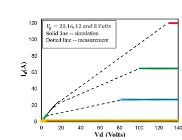
the saturation region and the channel current need to be correctly modeled. Figure 2-2 and Figure 2-3 are the TCAD simulation IV curve for a medium voltage and high voltage SiC MOSFET, suggesting that the saturation bias is much higher for high voltage SiC than for medium one.
This is due to the peak electric field, which is the cause of the velocity saturation, increases
slower in high voltage SiC with lower doping drift region according to Poisson equation.
This particular feature of high voltage SiC MOSFET – saturation voltage increases
drastically as the gate voltage increases – poses a challenge when it comes to fitting the IV
curves with relatively simple equations.
15 In 2007, a 2kV SiC MOSFET model [23] has been developed in SaberTM. The drift region
resistance is calculated based on the doping concentration provided by the vender and the
active area. Although the current spreading effect might not be significant given that it only
has 20 μm drift region, using only active area to calculate the resistance for longer drift region
(e. g. 100 μm) might be erroneous. In addition, in order to deal with the fact that the saturation
happens at higher drain bias for high voltage SiC MOSFET, the author in [23] propose
superposition of Imosh and Imosl to fit the total current. One component saturate at lower drain
bias and another saturate at higher drain bias. This results in more complicated current
16 to the model without superposition of two current components. Finally, the parameter
extraction procedure in the paper requires unique software that might not be easily accessible
to the public. In 2008, a 10kV MOSFET model in SPICE has been proposed. The MOSFET
equations being used are the SPICE level 1 model. The drift region resistance is fitted in a
behavior manner, and the saturation current is not discussed. For dynamic switching, a rather
complicated sub-circuit is used to describe the non-linear capacitance Cgd. In sum, the goal is
to develop a macro device model of 4H-SiC high voltage MOSFET for circuit simulation with
fairly simple current equation. The model will have the ability to describe the current in the
saturation region and fit the IV curves with the drastic increase of Vd,sat as gate voltage
increases.
2.2 On-state modeling of the proposed model
2.2.1 Drift region resistance
Accurately modeling of the drift region resistance is important especially for the high voltage device with a long drift region. Figure 2-4 shows the simple cross-section of the
MOSFET and the simplified equivalent circuit to describe the behavior during on-state.
17 Figure 2-5 illustrates the current conducting path from the back side to the top active area. The nominal chip size and active area are 64mm2 and 32mm2, respectively. The resistance
between the top and bottom metal should be calculating using the effective cross-section
marked using the red dashed line in Figure 2-5. Table 2.1 shows that it would be erroneous if
calculating Rdrift using the active area of 32mm2.
Noted that, however, the actual resistance can be up to 10% lower due to the fact that
there will be some fringing current outside the truncated shape indicated by the red dotted line.
The active area under low drain bias should be at least 45.3mm2. The estimated drift region
resistance at room temperature and low drain bias is 0.488 Ω. This initial estimated value will
be optimized within a 10% range of this estimated value together with other parameters in the
model.
Table 2.1 Resistance calculated using different methods.
𝐑𝐭𝐨𝐭𝐚𝐥(25oC)
(Measured)
𝐑𝐝𝐢𝐫𝐟𝐭(25oC)
(Calculated using active area)
𝐑𝐝𝐫𝐢𝐟𝐭(25oC)
(Calculated using effective active area)
0.627 Ω 0.703 Ω (not likely) 0.488 Ω
18 2.2.2 Velocity saturation in the drift region
The velocity saturation in semiconductor power devices happens near the area of high
electric field. For vertical power MOSFET, the current saturation mechanism might result from
the combination of two: (a) saturation in the channel and (b) saturation in the JFET region, or
quasi saturation. For high voltage device with lightly doped drift region, the saturation will
happen at higher drain bias, as depicted in Figure 2-6. To reach the peak electric field that
causes the velocity saturation, device with lightly doped drift region has to apply more voltage
to reach that value according to Poisson equation.
Figure 2-7 and Figure 2-8 plot electron velocity at varied drain bias for two SiC
MOSFETs with 4.5E15 and 1E15 cm-3 doping, respectively. At relatively low drain bias, the channel as well as the JFET region for 650 V MOSFET already reach velocity saturation,
19 Figure 2-8 Electron velocity plots of SiC MOSFET with ND=4.5E14 cm-3 at Vg=15 volts and Vdd= 1, 4, 6, 7.5 volts. Current start to saturate at Vdd=4 volts.
20 Figure 2-9 is the electron velocity versus the electric field in 4H-SiC, which indicates
that the velocity starts to saturate after the electric field of 1E5V/cm. Later in the derivation of
MOSFET current equation, the peak electric field of 1E5 V/cm is assumed to be the criteria of
velocity saturation.
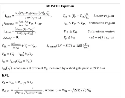
21 2.2.3 MOSFET current equation and its parameters
Linear region (𝑘𝑙, 𝑘𝑠, 𝜃, 𝑉𝑡ℎ):
The equation that describes voltage-current relationship in the linear region is given in tab.
III. The transconductance in the linear region at smaller drain bias is 𝑘𝑙, and ks serves as a
correction term to gradually modulate the transconductance as the drain bias increases. The
effect of channel mobility as a function of vertical electric field in the channel is modeled by
the parameter 𝜃𝑙. These parameters will be directly fitted later using the measurement results.
The threshold voltage Vth can be estimated using Vgs – Id curve and will be optimized later
along with the other parameters.
MOSFET Equation
Id,lin =
kl× Vg−Vth ×Vch−12×Vch2 ×kskl
1+𝜃𝑙(𝑉𝑔−𝑉𝑡ℎ) , 𝑉𝑐ℎ< 𝑉𝑔− 𝑉𝑡ℎ
kl
ks 𝐿𝑖𝑛𝑒𝑎𝑟 𝑟𝑒𝑔𝑖𝑜𝑛
𝐼𝑑,𝑡𝑟𝑎𝑛𝑠.=𝑉𝑑ℎ−𝑉𝑑𝑙
𝐼𝑑ℎ−𝐼𝑑𝑙 𝑉𝑐ℎ+ 𝐼𝑑𝑙, 𝑉𝑑𝑙≤ 𝑉𝑐ℎ≤ 𝑉𝑑ℎ 𝑇𝑟𝑎𝑛𝑠𝑖𝑡𝑖𝑜𝑛 𝑟𝑒𝑔𝑖𝑜𝑛
Id,sat =
1
2𝑘𝑚𝑎𝑥. 𝑉𝑔−𝑉𝑡ℎ 2
1+𝜃𝑠 𝑉𝑔−𝑉𝑡ℎ , 𝑉𝑐ℎ≥ 𝑉𝑑ℎ 𝑆𝑎𝑡𝑢𝑟𝑎𝑡𝑖𝑜𝑛 𝑟𝑒𝑔𝑖𝑜𝑛
𝐼𝑑,𝑜𝑓𝑓 = 0, 𝑉𝑔≤ 𝑉𝑡ℎ 𝑐𝑢𝑡 − 𝑜𝑓𝑓 𝑟𝑒𝑔𝑖𝑜𝑛
Vdh=𝜀𝐸𝑐𝑜𝑟𝑛𝑒𝑟2
2𝑞𝑁𝐷 + 𝑉𝑔− 𝑉𝑡ℎ, Ecorner(4𝐻 − 𝑆𝑖𝐶) ≅ 1𝐸5 (
𝑉 𝑐𝑚)
Vdl= 𝑉𝑔− 𝑉𝑡ℎ 𝑘𝑙 𝑘𝑠
Idl = 𝐼𝑑,𝑙𝑖𝑛(𝑉𝑐ℎ = 𝑉𝑑𝑙)
Idh 𝑉𝑔 is constants at different Vg, measured by a short gate pulse at 2kV bias KVL
Vd= 𝑉𝑐ℎ+ 𝑅𝑑𝑟𝑖𝑓𝑡× 𝐼𝑑
Rdrift= 𝑞𝑁1 𝐷𝜇𝑛
𝐿
𝐴𝑎𝑐𝑡𝑖𝑣𝑒×𝐴𝑐ℎ𝑖𝑝 , where L = WD − 2𝜀𝑉𝑐ℎ 𝑞𝑁𝐷
22 Figure 2-10 shows that the Vds-Id curve at low gate bias at different temperature, and
clearly the threshold voltage decreases with temperatures. The estimated threshold voltage
ranges from 5.3 volts at room temperature to 3.5 volts at 125oC. After the initial estimation of some parameters, the fitting is conducted in EXCEL by finding the sum of the least square root
between the calculated and measured data points, as shown in Figure 2-11. The initial
estimation is necessary to avoid the iteration of finding the minimum ending up converging to
local minimum instead of global minimum.
23
Figure 2-12 shows the simulated and measured I-V curve at different gate voltage at room temperature. Figure 2-13 shows the model can predict that the on-state conductance is lower at elevated
Figure 2-11 Parameters optimization by iterating to find the minimum sum of least square root.
24 temperature. Figure 2-14 is the extracted threshold voltage and transconductance as a function
of temperature.
Figure 2-14 Transconductance in the linear region and threshold voltage as a function of temperature.
25 Saturation region (𝑘𝑚𝑎𝑥, 𝜃𝑠):
MOSFET current at higher bias is assume to be a constant in this model. The saturation
region is defined as the peak electric field excees 1E5 V/cm, as pointed out in Figure 2-6 The
illustration of the difference between E field in low and high doping drift region. The measured
saturation current level at different gate bias is obtained by give a gate pulse at Vd=2k [7]. The
equation in this region is provided in tab. III. By using the same parameter optimization manner
introduced earlier, the fitted transconductance in the saturation region and θs are shown in
Figure 2-15.
26 For low-to-medium voltage MOSFET behavior modeling, using only two region can
smoothly fit the model with the measurement results for a wide gate bias range. However, it is
difficult for high voltage SiC MOSFET due to the fact that the difference between the
saturation voltage at high gate bias and low bias is too large, as evidenced in Error! Reference
ource not found. and Error! Reference source not found. (15kV and 650kV) plotted using TCAD simulator, in which the parameter file in the channel region of the software are identical.
This make it difficult to fit the curve using only linear and saturation region in a wide range of
gate bias. Therefore, a transition region must be introduced between the linear and saturation
region. This region also known as quasi-saturation region [24], in which the voltage drop
across the depletion region prevent the end of the channel from perceiving the high electric
field. Nevertheless, the current (and the electron velocity) will still gradually saturate due to
the velocity saturation in the depletion region of the drift region.
Transition region (quasi-saturation):
In [23], two current components Imosh and Imosl, are superposed in the linear region to
smoothly connects the linear region and saturation region. In this proposed model, a simpler
way of describing this region is to connect the linear region and the saturation region with a
straight line. Although losing certain fidelity in this region is inevitable, from a practical point
27 The boundaries between linear/transition region (vdl) and transition/saturation region (vdh)
have to be defined. The linear region at corresponding gate voltage ends when the derivative
of the I-V curve is zero. The saturation region starts when the peak electric field in the drift
region reaches 1E5 V/cm2. The equations and relations are provided in Table 2.2, and the final IV curves across three regions are shown in Figure 2-16.
2.3 Dynamic switching modeling
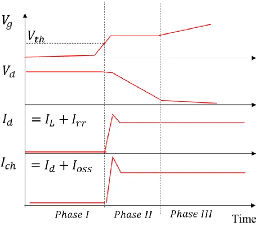
2.3.1 Switching dynamics during turn-on
Figure 2-17 shows three phases during turn-on transient and the current flows. Figure
2-18 shows the corresponding voltage and current waveforms.
28 Figure 2-17 Turn-on transient and current flows. Solid and dashed lines are the conduction and displacement current, respectively.
29 Phase I:
This phase is defined before the gate voltage reaches the threshold voltage. The gate current
is charging the Cgs through gate resistances. The non-linear Cgs will decrease from its
maximum capacitance C𝑚𝑎𝑥. at negative gate voltage to its minimum capacitance value
Cmin. when the gate voltage increases toward threshold voltage. Therefore, the gate voltage
charging trajectory is slow (delay) and then fast. The channel remains off during this phase
while the load current floating through the freewheeling diode.
Phase II:
Once the gate voltage rises above the threshold voltage, the channel starts to turn-on, and the channel current rises. When the gate voltage reaches the “Millar plateau,” the drain voltage
will start to rise, while gate current will flow mostly through Cgd. Noted that due to the dv/dt
presents at the drain node, there will be displacement current flow from the capacitance of the
diode. Also noted that the total current that flow through the channel is the sum of ioss, IL and
Irr. The displacement current that discharge the output capacitance (ioss) is an internal current
that cannot be measured at the drain node. But this current component will contribute to the
total turn-on loss.
Phase III:
After the drain voltage decrease to the on-state voltage drop at the gate plateau voltage, the
gate current stops flowing through Cgd and starts to further overdrive Cgs until the gate voltage
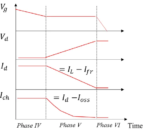
30 2.3.1 Switching dynamics during turn-off
Figure 2-19 Turn-on transient and current flows. Solid and dashed lines are the conduction and displacement current, respectively.
31 Phase IV:
The gate current slowly discharges Cgs before the gate voltage reaches the Miller plateau. The drain voltage will slightly increase due to the increase of channel resistance.
Phase V:
When the gate voltage reaches certain value (plateau), the channel current is not large
enough to carrier all the load current. Part of the load current will start to charge the capacitance
seen by the drain node – output capacitance of the MOSFET as well as the diode. The current
measured at the drain node will decrease since part of the load current has been stolen by the
diode output capacitance due to the presence of dv/dt. Noted that, internally, the current
flowing through the channel is even smaller and is equal to the drain current minus the current
that charging the MOSFET output capacitance.
Phase VI:
When the drain voltage exceeds the bus voltage plus the forward voltage of the diode,
the diode starts to turn on. The drain voltage will remain constant and the gate current will
32 2.3.2 Extraction of parasitic capacitance
Output capacitance (Coss):
The output capacitance is composed of Cds and Cgd. It can be obtained by giving a current
pulse and directly measuring the dv/dt with the gate and source shorted. Alternatively, one can
switch two parallel devices with the DUT’s gate and source connecting to the ground. The
output capacitance of the DUT can then be obtained by dividing the current flowing through it
by dv/dt.
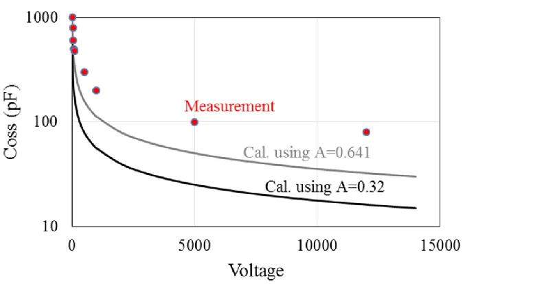
Since the device active area (32mm2) and chip size (64mm2) are known, it is interesting to
compare the calculated and extracted results, as shown in Figure 2-21. Surprisingly, even
calculated using the total chip size area, the calculated output capacitance is still two times
smaller than the actual measured results. The difference of the capacitance value may come
from package capacitance, fringing effect and 2-D effect while the depletion region
expanding/retrieving in the edge termination area. In other words, these secondary effect
makes it harder to charge/discharge the overall capacitance than a 1-D ideal capacitance, and
33 Crss (reverse transfer capacitance):
Also known as the gate-to-drain capacitance, this capacitance can be extracted by dividing the
gate current during the Miller plateau by the dv/dt during turn-on.
Ciss (input capacitance)
This capacitance consists of Cgd and Cgs. Since Cgd has been extracted, we will only discuss
the extraction of Cgs. A typical Cgs as a function of gate voltage is depicted in Figure 2-22. The
Cmax is extracted by using the Vg-t curve in phase III during turn-on. The Cmin. is extracted
by using the Vg-t curve in phase I during turn-on.
34 The C-V curves for the 10A 15kV 4H-SiC MOSFET with a 32mm2 active area is shown in Figure 2-23.
Figure 2-22 Typical CV curve for the input capacitance of a MOSFET.
35
2.4 Model implemented in Simulink/Matlab
Simulink/Matlab is a powerful software that allows model developer to write the equations
in the user-defined box to describe the device behavior. For example, the MOSFET equation
in tab. III are directly written in the user-defined box to serve as a voltage-controlled current
source. The implementation of non-linear capacitance can be done by building a look-up table,
in which the capacitance as a function of the voltage can be directly plotted. This means no
cumbersome equation is needed to account for the secondary effect of the capacitance (for
example 2-D effects). The capacitor implementation is shown in Figure 2-24, in which the
1-D look up table is where the user can directly draw or key in the capacitance value as a function
of voltage.
36 The final model is shown in Figure 2-25.
37 Figure 2-26 shows the simulation setup of double pulse test circuit. Ode 15 is used for simulation in the Simulink/Matlab to get fast and easy-to-converge result.
38
2.5 Model validation
The simulated results will be compared to the measurement results for inductive switching for both turn-on and turn-off. The circuit simulation will also include a simple
Schottky diode model, whose parameters are extracted from a real device that is used in
the measurement. Figure 2-27 and Figure 2-28are the turn-off and turn-on result comparison, respectively.
39 The turn-on energy loss as a function of current predicted by the proposed model is
shown in Figure 2-29. Most importantly, this model accounts for the loss related to energy
stored in the output capacitance, as discussed in section 2.3.1. Also known as Eoss, this loss
cannot be directly measured and is important to include when estimating the turn-on loss. Since
the charge and discharge of the capacitance do not consume power, it is the current that flow
through the resistors, such as channel resistance or partially depleted drift region during the
40 Figure 2-30 and Figure 2-31 show the model’s prediction of the energy loss as a
function of current at 25oC and 125oC, respectively. The DC bus voltage is 9kV and the gate resistance is 10 ohm. Notice that these simulated results do not include the Eoss but simply the
power calculated using the terminal current and the voltage of the device.
41 Figure 2-31 Energy loss versus current prediction at 125oC. VDD=9kV.
42 Figure 2-32 is the total switching loss prediction by the model, showing excellent match
between the simulated and measured results.
43
Chapter 3
20A 15kV 4H-SiC n-IGBT Modeling
20A 15kV 4H-SiC n-IGBT Modeling
3.1 Review of IGBT model
Due to the presence of the excess carrier, modeling ambipolar devices is more challenging
than unipolar devices. In general, IGBT model can be categorized in two ways: the manner of
implementing the model and handling the excess carriers in the drift region. It is summarized
in Table 3.1.
44 3.1.1 Hefner’s model (E.D.C)
The most classic modeling work is proposed by Hefner in [18] and later implemented in
saber [26]. This work can be categorized as an E.D.C (equivalent-circuit dynamic charge)
model according to the definition in Table 3.1. The equivalent circuit model is depicted in
Figure 3-1.
45
Noted that an IGBT model will become a MOSFET model when the quasi-neutral base
region in Figure 3-1 is removed. The left leg of the model is the hole current path while the
right one is the electron current path. It can be seen that the amount of the current that charges
the Cgd and Cds are smaller in IGBT than in MOSFET. This is because the current that actually
goes to Cgd and Cds in IGBT is total current minus the current flow through collector current
(Jc) and redistribution current (Credist.𝑑𝑣/𝑑𝑡).
The center-piece of Hefner’s model is the redistribution capacitance Credist., or Ccer. The
origin of this capacitance is depicted in Figure 3-2 and the detail derivation is in [18].
It basically describes that when the depletion boundary pushes the excess carrier
plasma, there will be a counter-force that slows down the retreating of the depletion boundary
due to the presence of excess carrier plasma.
46 In D. C. (dynamic charge) model, there is only one big node being placed in the drift region
and another in the buffer layer. The equation that governs the charge dynamic is based on
charge continuity equation and Boltzmann’s Junction Law. Fore non-punch through, the
equation is given by:
𝑑𝑄 𝑑𝑡 = −
𝑄 𝜏 −
𝑄2 𝑄𝐷2
4𝑁𝑠𝑐𝑙2
𝑛𝑖2 𝐼𝑠𝑛𝑒 + 𝑖𝑑+ 𝐼𝑀𝑂𝑆 (3.1)
Once the total charge is obtained, the carrier is assumed to be linear, as the solid line shown in
Figure 3-2. This assumption is somehow valid if the depletion region is not moving, for
example, during the current decaying phase; however, if the boundary is moving (pushing the
excess carrier into quasi-neutral base region), according to Hefner, there will be a redistribution
carrier profile component that will be superposed on this linear carrier. The redistribution
carrier profile is then lead to an extra current component and can be modeled using a
redistribution capacitor Credis:
Credis = 𝐶𝑏𝑐𝑗 𝑄(𝑡)
3𝑞𝑁𝐷𝐴(𝑊 − 𝑥𝑑) (3.2)
It is reported in [27, 28] that this capacitance might be the cause of the unrealistic ringing of
the model. This capacitance is even abruptly incorporated in other model [27, 28] to account
for this phenomenon.
In fact, if enough nodes were placed throughout the drift region to modeled the dynamic
47 redistribution component would not have to be included in the model. However, placing too
much nodes may significantly slow down the computation speed of the model.
The KCL of this model is given by [18]:
IT= 1 1 + 𝑏 𝐼𝑇+
2𝐷𝑎
𝑊2AQ(t) + Credist.
𝑑𝑉
𝑑𝑡 +IMOS+ 𝑖𝑔𝑑+ 𝑖𝑑𝑠 (3.3)
48 3.1.2 Lumped charge model (E. L. C.):
One way of modeling the ambipolar devices, including PiN [29], GTO [30] and IGBT [27], is the lumped charge model. All the lumped charge models in recent years have been added
the displacement current in the continuity equations in the models. The methodology is to
deploy charge nodes at critical position in a device. This model type can be categorized in E.
L. C in Table 3.1. For a non-punch through structure, it only takes 5 nodes – three in the drift
region and two nodes at the junction in the emitter and the collector. However, only one ODE
has to be solved in the drift region. Figure 3-3 depicts the carrier dynamics at low and high
reverse bias during turn-off.
From Figure 3-3, it can be observed that using three nodes along is not sufficient to model the boundary of the carrier density profile near the depletion region, especially when the
49 neutral base is long at low reverse bias. This will lead to erroneous calculation of the hole
current entering from quasi-neutral base region to the depletions region. In this sense, devices
with long drift region (high voltage) are not suitable for this modeling technique. Although
using the parameter fitting techniques might lead to decent match of the switching waveform,
the carrier dynamics and the physical parameters might be totally different from the real case
in order to compensate the insufficiency of this model in predicting carrier dynamics.
For current high voltage 4H-SiC IGBT technology, the punch through happens around
half of the DC bus voltage [31]. In addition, the buffer layer in the structure not only serves as
a field stop layer but also a valve to adjust the carrier injection. This means that in order to
model the high voltage 4H-SiC IGBT, it requires at least 8 nodes deployed in the structure –
three in the drift, three in the buffer (has to be so in order to model recombination in the buffer)
and two in the emitter and the collector. Moreover, the carrier dynamic during the transition
right before and after punch through can be complicated to handle.
3.1.3 Fourier-series-based model:
The techniques of this model is to use the Fourier-series as a solution of PDE that describe
the carrier density profile. The boundary conditions of the profile are from the currents that
enter/leave the quasi-neutral base region. This method is first proposed in [32]. In 2007, an
IGBT model has been developed using this techniques [22].This model is depicted in Figure
50
Notice that this model also emulates the contraction of the carrier profile during turn-off
near the drift region. This is a similar feature captured in Hefner’s model, in which he uses the
“redistribution current” or the redistribution capacitance (Ccer) [18] to achieve this feature.
Since Fourier-series-based model already capable of predicting the sharp bend of the carrier
density profile near the depletion region using Fourier-series, and therefore, do not require any
imaginary component like redistribution current to describe this transition region.
The mathematical nature of this techniques, however, may limit the implementation of the
model into software such as PSPICE. In addition, mathematical models are proprietary to the
developers and can be complicated to develop, especially for engineer with circuit background,
mainly because equivalent circuit model is more systematically connected by utilizing the KCL
and KVL that is inherently embedded in most of the software such as Simulink, PSPICE and
51 convergence issues [22]. In determining the depletion region, a large negative feedback loop
that has no physical meaning, as shown in Figure 3-4, is used to constantly keep the boundary
carrier density near the depletion region (px2) to be zero while the depletion voltage is
generated. While other models need the depletion width and voltage first to calculate the new
carrier profile for each time step, this model backwardly calculate the carrier profile first and
then use the trick mentioned above to obtain the voltage across the depletion region.
Based on the discussion above, equivalent-circuit model seems to be preferable to the
mathematical model. This means the Fourier-series-based model is opted out toward
52
3.2 IGBT theory and principle
Figure 3-5 and Figure 3-6 summarize the preliminary theories in the quasi-neutral
base region that will be used in the on-state modeling of IGBTs.
Figure 3-5 Device physics during on-state that will be discussed in the section.
53 3.2.1 Ambipolar diffusion equation at arbitrary injection level
Ambipolar transportation is used to describe the electron and hole current in the presence
of each other. The derivation of the expression of the current under the high-level injection can
be found in [11]. Here the ADE under more general cases are provided under arbitrary injection
level.
For n channel device:
Jn = 𝑏(1 + 𝜆)
1 + 𝑏(1 + 𝜆)𝐽𝑇− 𝑞 2 + 𝜆
2
1 + 𝑏
1 + 𝑏(1 + 𝜆)𝐷𝑎 𝜕𝑝(𝑥)
𝜕𝑥 (3.4)
Jp =
1
1 + 𝑏(1 + 𝜆)𝐽𝑇+ 𝑞 2 + 𝜆
2
1 + 𝑏
1 + 𝑏(1 + 𝜆)𝐷𝑎 𝜕𝑝(𝑥)
𝜕𝑥 (3.5)
For p channel device:
Jn = 𝑏
1 + 𝑏 + 𝜆𝐽𝑇− 𝑞 2 + 𝜆
2
1 + 𝑏 1 + 𝑏 + 𝜆𝐷𝑎
𝜕𝑛(𝑥) 𝜕𝑥
(3.6)
Jp = 1
1 + 𝑏 + 𝜆𝐽𝑇+ 𝑞 2 + 𝜆
2
1 + 𝑏 1 + 𝑏 + 𝜆𝐷𝑎
𝜕𝑛(𝑥) 𝜕𝑥
(3.7)
λ(x) = 𝑏𝑎𝑐𝑘 𝑔𝑟𝑜𝑢𝑛𝑑 𝑑𝑜𝑝𝑖𝑛𝑔