Implementation of Dual Booting Module of
Convolution Encoder and Viterbi Decoder
Rakhi B. Menon1, Dr. Gnana Sheela K.2
M.Tech Student, Department of ECE, TOCH Institute of Science &Technology, Arakkunnam, Ernakulam, Kerala,
India 1
Professor, Department of ECE, TOCH Institute of Science &Technology, Arakkunnam, Ernakulam, Kerala, India2
ABSTRACT: Simulation of Convolution encoder and Viterbi decoder is done with the help of Model Sim. RTL view and Schematic view is obtained after the synthesis using Xilinx ISE tool. Detailed analysis of power and memory utilization is obtained using Altera Quartus software. Finally the encoder and decoder is implemented using dual booting module on Spartan 3E FPGA kit. On changing the position of switch, the same board works as convolution encoder and viterbi decoder. The decoding technique used is soft decision Viterbi decoding and it provides better accuracy for the decoded information.
KEYWORDS: Convolution encoder, Viterbi decoder, Simulation, Model Sim, Synthesis, Xilinx ISE tool, Dual booting module
I. INTRODUCTION
Codes are classified as Block codes and Convolutional codes. The block codes can be applied only for the block of data but the convolutional coding can be applied to a continuous data stream as well as to blocks of data. A convolutional code works by adding some structured redundant information to the user’s data and then correcting errors using this information. The difference between block codes and convolutional codes lies in encoding principle .In block codes, information bits are followed by parity bits. For convolution codes, information bits spread along the sequence. Also different is the utilization of memory elements in the convolutional encoders. In the case of block codes, there is no memory element involved in the generation of encoded data.
II. CONVOLUTION ENCODER
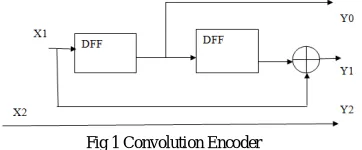
A convolution coding is done by combining fixed number of input bits. The input bits are stored in fixed length shift registers and combined using mod-2- adders. This operation is equivalent to binary convolution and hence it is called convolution encoding. Convolutional codes were introduced in 1955 by Peter Elias. Every two bits of a data stream are encoded into three bits for transmission. The ratio of input to output is called rate of encoder; thus it is a 2/3 encoder. The three outputs are calculated by:
Y2 = X2
Y1 = X1⋀D2
Y0 = D1
Fig 1 Convolution Encoder
convolution code is much more complex task. Several classes of algorithm exist for this purpose: Threshold decoding, sequential decoding and Viterbi decoding. Threshold decoding is the simplest of all the decoding, error correction capability is far from optimal and it can be applied only to a specific class of convolution codes. Sequential decoding is better than threshold decoding, it has unpredictable decoding latency, its error correction capability is sub optimal and is complex to decode. Immediate data delivery, high speed, high throughput, good error correction capability and no need for retransmission viterbi decoding is found to be the best of all decoding techniques.
III.VITERBI DECODER
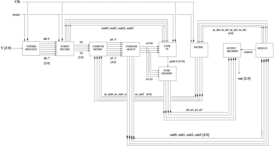
The Viterbi algorithm is named after Andrew J. Viterbi, who proposed it in 1967 as a decoding algorithm for convolutional codes. The Viterbi decoder consists mainly of four major blocks: Branch Metric Unit, Path Metric Unit, Add- Compare- Select Unit and Survivor Memory Management Unit. The internal modules of Viterbi decoder are: Viterbi distance calculation Module, Subset Decode Module, Compute Metrics Module, Compare Select Module, path memory Module, path in Module Metrics Module, Reduce Module and Output Decision Module.The received signal is converted into a series of distance measures from the known eight possible transmitted signals. The digitally encoded 3-bit signal, Y, from the encoder is converted directly to the distance measures. d[N] is the distance from signal = (2*sin(N*PI/8)) in 3-bit binary. Subset module chooses the signal corresponding to the smallest of each set {0,4},{1,5},{2,6},{3,7}.Therefore there are eight input signals dis0 to dis7 and four signals S0 to S3 are given as input to compute metric and Sout0 to Sout3 are given as the input to path in module.
Output of Subset decodes Module and output of Metric module is fed into the Compute Metric module. Eight paths are generated and is given to compare select module and it selects the path with minimum value. Path Metrics and Branch Metrics are added together here. Sum of branch metric and path metric is compared and minimum of the value is selected by Compare Select module. Control signals from the subset decoder and ACS modules are used to store the correct signal. Inside the path in module there are 12 different paths and this module decides the path. Path memory module consists of an array of memory elements that store and shift the path as new signals are added to the four paths. The registers created in this module store the four path metrics. Each register is 5 bits wide. Reduce module reduces the metrics after the addition and comparison operations. This module selects the smallest metrics and subtracts it from other metrics. Output decision decides the output signal based on path that corresponds to smallest metric.
IV.LITERATURE REVIEW
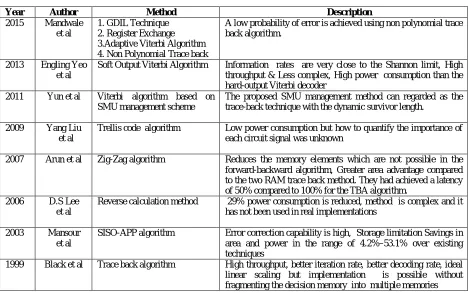
Different methods of Viterbi decoding techniques are compared and soft decision Viterbi decoding algorithm based on trace back method was found to be the best of all. In the case of hard decision Viterbi decoder, the only possible values are 0 and 1. But for a soft decision Viterbi decoder, wide ranges of values such as 0, 0.2, 0.4, 0.7,1 are possible and thus ensures more accuracy for the decoded values.
Mandwale et al (2015) compared four different approaches [1]
Method I: GDIL Technique: GDIL technique is introduced for low area consumption and for reducing delay of the circuit. By comparing GDIL with other traditional CMOS and various pass-transistor logic design techniques less area consumption for GDIL is achieved. With the GDIL approach we can design the wide range of complex logic functions using minimum transistors. This method gives us fast speed, low-power consumption circuits, using minimum number of transistors as compared to other techniques like CMOS and Pass transistor logic design.
Method II: Register Exchange: This is mainly concentrated on light-weighted pipelined serial Viterbi Decoder design for resource saving purpose. The trace back bits are stored in RAM unit instead of register array and TBU is not needed. Also for string the BMU and ACS values ‘Metric RAM’ is used.
Method III: Adaptive Viterbi Algorithm: Instead of saving data in RAM, data is stored in buffers for designing path storage block. For reducing the time when performing branch metric calculation parallel processing is done with Hamming distance. While designing the ACS unit, ROM and 3bit to 12bit shift register is considered.
Method IV: Non Polynomial Approach: A low probability of error is achieved in this Viterbi decoder paper using non polynomial approach. For BMU, it compares the received bits with expected bits. While designing the ACS unit, the addition of path metric and then subtraction is done for purpose.
Engling Yeo et al (2013) [2] compared four different structures for the implementations of the ACS recursion. These inferences are applicable to the implementations of both soft and hard - decision Viterbi decoders. It was found that architectural retiming and transformation of the ACS structures with modification of the register exchange provided the highest throughput without excessive area and power penalties. Although the SOVA has less complexity than the MAP decoder, it still has higher power consumption than the hard- output Viterbi decoder. In practical high performance iterative decoders, the power could be lowered through custom circuit design and technology scaling. Yun et al (2006) described a novel low - power design methodology of Viterbi decoder. Based on the described SMU management scheme, [3] the number of memory access could be significantly reduced, that could help to reduce the power consumption. The studied SMU management could also be regarded as the trace-back technique with the dynamic survivor length. Yang Liu et al (2009) [4] discussed Design of voltage over scaled low-power trellis decoders in presence of process variations. Unequal error tolerance involved two main issues i.e. how to quantify the importance of each circuit signal and how to incorporate the importance qualification into signal processing circuit designs.
Arun et al (2007) [5] minimized memory architecture for low latency Viterbi decoder using Zig-Zag algorithm. In forward backward algorithm, when employed in sliding window technique, the time slot is properly utilized to reduce the memory elements. The data storage takes place always in the forward manner and the trace back in reverse manner. Whereas in the Zig-Zag algorithm, storage takes place from right to left in the forward direction and trace back from left to right in the reverse direction but it is exactly opposite in the second time and vice-versa which reduces the memory elements which is not possible in the forward-backward algorithm. The proposed method provided greater area advantage compared to the two RAM trace back method. They had achieved a latency of 50% compared to 100% for the trace back algorithm. Dong-Soo Lee et al (2006) [6] implemented approximate reverse calculation method for backward metrics with simple arithmetic operations such as addition and comparison .They achieved the access rate of the backward metric memory by 87% in W-CDMA standard without affecting error correcting performance. 29% power consumption was reduced in a log- MAP decoder by employing the approximate reverse calculation method.
radix-2 state parallel Viterbi decoder could be increased by using higher radix formulations of the trellis. Implementation of trace-back algorithm using pre-traced decision was possible without fragmenting the decision memory into multiple memories and without running multiple trace-back recursions in parallel.
Table 1 Comparison of Viterbi decoding techniques
Year Author Method Description
2015 Mandwale et al
1. GDIL Technique 2. Register Exchange 3.Adaptive Viterbi Algorithm 4. Non Polynomial Trace back
A low probability of error is achieved using non polynomial trace back algorithm.
2013 Engling Yeo et al
Soft Output Viterbi Algorithm Information rates are very close to the Shannon limit, High throughput & Less complex, High power consumption than the hard-output Viterbi decoder
2011 Yun et al Viterbi algorithm based on SMU management scheme
The proposed SMU management method can regarded as the trace-back technique with the dynamic survivor length.
2009 Yang Liu et al
Trellis code algorithm Low power consumption but how to quantify the importance of each circuit signal was unknown
2007 Arun et al Zig-Zag algorithm Reduces the memory elements which are not possible in the forward-backward algorithm, Greater area advantage compared to the two RAM trace back method. They had achieved a latency of 50% compared to 100% for the TBA algorithm.
2006 D.S Lee et al
Reverse calculation method 29% power consumption is reduced, method is complex and it has not been used in real implementations
2003 Mansour et al
SISO-APP algorithm Error correction capability is high, Storage limitation Savings in area and power in the range of 4.2%–53.1% over existing techniques
1999 Black et al Trace back algorithm High throughput, better iteration rate, better decoding rate, ideal linear scaling but implementation is possible without fragmenting the decision memory into multiple memories
V. SIMULATION OF ENCODER AND DECODER
Codes of Convolution encoder and Viterbi decoder and their test benches is written in Verilog HDL and is simulated using Altera Model Sim. Simulator is a software program to verify functionality of a circuit. The functionality of code is checked. The inputs are applied and corresponding outputs are checked. If the expected outputs are obtained then the circuit design is correct. Simulation gives the output waveforms in form of zeros and ones. Here arises what is called RTL diagrams.
Fig 3. Simulation of convolution encoder
System C, and includes a built-in C debugger. ModelSim can be used independently, or in conjunction with Altera Quartus or Xilinx ISE.
VI.SYNTHESIS OF ENCODER AND DECODER
An intermediate representation of the hardware design is produced. This step is called synthesis and the result is a representation called a net list. Once the functional verification is done, the RTL model is taken to the synthesis process using the Xilinx ISE tool. In synthesis process, the RTL model will be converted to the gate level netlist mapped to a specific technology library. In this step, any semantic and syntax errors are checked. The synthesis report is created which gives the details of errors and warning if any.
Fig 4. RTL view of Convolution encoder and Viterbi decoder
The RTL (Register Transfer Logic) of Convolution encoder is shown in first figure, where an input of two bits is provided to the encoder along with clock and reset. Three bit values are obtained as output. The RTL of Viterbi decoder is shown in second figure, where an input of three bits is provided to the encoder along with clock and reset. Two bit values are obtained as output along with an error bit. If the error bit is 0, there are no errors occurred. When the error bit is 1, it indicates the presence of errors.
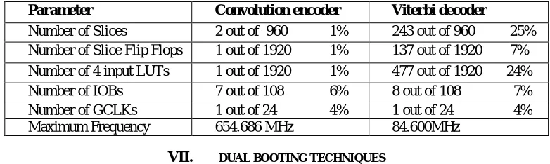
Table 2 Comparison of Device utilization memory of Convolution encoder and Viterbi decoder
Parameter Convolution encoder Viterbi decoder
Number of Slices 2 out of 960 1% 243 out of 960 25%
Number of Slice Flip Flops 1 out of 1920 1% 137 out of 1920 7%
Number of 4 input LUTs 1 out of 1920 1% 477 out of 1920 24%
Number of IOBs 7 out of 108 6% 8 out of 108 7%
Number of GCLKs 1 out of 24 4% 1 out of 24 4%
Maximum Frequency 654.686 MHz 84.600MHz
VII. DUAL BOOTING TECHNIQUES
Fig 5 Multiple booting technique- a) Convolution encoder b) Viterbi decoder
VIII. IMPLEMENTATION RESULTS
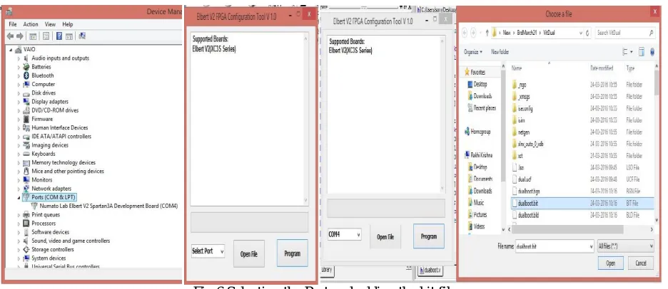
In order to select the port, device manager of the computer is to be checked whenever the kit is connected as the port varies over time. Here, as shown in the figure Numato Lab Elbert V2 Spartan 3A Development Board (COM4) means that the port that must be selected is COM 4. The next step is to select the Port which must be the same as shown by the device manager. So COM 4 is selected and corresponding bit file is added.
Fig 6 Selecting the Port and adding the bit file
Fig 6 Loading the files
Working as Convolution Encoder: The button is turned on and the value is made ‘0’. Results are obtained both on Leds and Seven Segment display. The figure shows the implementation of a convolution encoder of rate ½. The decoded two bit outputs are visible both on LCD as well as indicated by LED.
Working as Viterbi decoder: The button is turned off and the value is made ‘1’. Results are obtained both on Leds and Seven Segment display. The output of the encoder is given as input of Viterbi decoder
.
The output obtained from decoder matches with the input of encoderFig 8 Implementation of Viterbi decoder of rate 2/1
IX.CONCLUSION AND FUTURE WORK
Simulation of Convolution encoder and Viterbi decoder is done with the help of Model Sim. RTL view and Schematic view is obtained after the synthesis using Xilinx ISE tool. Detailed analysis of power and memory utilization is obtained using Altera Quartus software. Finally the encoder and decoder is implemented using dual booting module on Spartan 3E FPGA kit. On changing the position of switch, the same board works as convolution encoder and viterbi decoder. In future, encoder and decoder of higher rates can be implemented using multiple booting techniques
REFERENCES
1. Mandwale A. J and Mulani A O” Different Approaches For Implementation of Viterbi decoder on reconfigurable platform” International Conference on Pervasive Computing (ICPC) 2015
2. Engling yeo, Augsburger, S.A., Rhett Davis, W. and Borivoje Nikolic . “ A 500-Mb/s soft-output Viterbi decoder”, IEEE Journal of solid-state circuits ,Vol. 38, No. 7, pp. 1234-1241,2013
3. Yang Liu, Tong Zhang and Jiang Hu. “Design of voltage over scaled low-power trellis decoders in presence of process variations”, IEEE Transactions on Very Large Scale Integration (VLSI) systems, Vol.17 , No.3, pp. 439-443, 2009
4. Arun, C. and Rajamani, V. “Minimized memory architecture for low latency Viterbi decoder using Zig-Zag algorithm”, International Journal on Wireless and Optical Communications (IJWOC), Vol.4, No.3, pp. 313-323, 2007
5. Jameel Hussein, "Multiple-Boot with Platform Flash PROMs", Application Note on Spartan-3E FPGA, Xilinx Company, April 2007 6. Lee, D.S. and Park, I.C., “Low-power log-MAP decoding based on reduced metric memory access”, IEEE Transactions on Circuits and
Systems, Vol.53, No.6, pp.1244-1253, 2006
7. Ken Chapman, "NOR FLASH Programmer for Spartan-3E Starter Kit", User Guide Xilinx Ltd., March 2006 8. S. Haykin M. Moher, “Modern wireless communications”, Printice Hall,2005
9. Mohammad M. Mansour and Naresh R. Shanbhag. “VLSI Architectures for SISO-APP Decoders”, IEEE Transactions on very large scale integration (VLSI) systems, Vol. 11, No. 4, pp 627-650, 2003
10. Peter, J. Black and Teresa, H . Meng, “A 140-Mb/s, 32-state. Radix4 Viterbi Decoder”, in: Proceedings of the IEEE Journal of Solid State Circuits, Vol.27 , No.12, pp.1877- 1885, 1993
11. Proakis, J.G., Digital Communications, 2nd Ed., McGraw-Hill, 1989
BIOGRAPHY
Rakhi B. Menon completed her B.Tech in Electronics & Communication Engineering under Mahatma Gandhi University. Currently she is pursuing M.Tech in the specialization of VLSI and Embedded System of CUSAT.