ABSTRACT
YU, YILING. Engineering Light Matter Interaction of Atomically Thin Transition Metal Dichalcogenide Materials. (Under the direction of Linyou Cao.)
The study on class of atomically thin metal dimensional transition metal dichalcogenide
materials (TMDC) is growing fast. The distinct electronic and optical properties of this
material direct point to its application in the new generation of real atomically thin devices.
Since it is relative new class of materials, a lot of fundamental physical problems which
relate to the origin of its novel properties still need to be answered for this new emerging low
dimensional material. In another hand, there are also many problems need to be solved regard
to reaching high performance of the TMDC devices in real applications. Our focus is to
study TMDC for understanding and engineering their strong light-mater interactions. This
can be both fundamentally and practically important to TMDC nanophotonics.
We systematically studied two light-matter interaction processes of TMDC: absorption,
reflection, transmission process and light emission process. The two processes are key for
realizing TMDC photonic devices in different applications. For the light absorption process,
we measured the layer dependent optical dielectric function of MoS2 films for the first time
and demonstrates the dielectric function is dominated by excitonic effect rather than
electronic band structure. Based on this conclusion, we further realize giant tunability of
refractive index of monolayer TMDC by applying electrical gating field and revealed more
complex underlying mechanisms. These two work no doubt pave a new way to realize
CMOS compatible electro-photonic devices for atomically thin TMDC. For the light
emission process in monolayer TMDC, we revealed the intrinsic limitation for TMDC is the
power for population inversion for monolayer TMDC, which is the first step to making Laser.
We also thoroughly investigated the effect of substrate to the light emission efficiency, which
is the most important external environment factor. Get to the conclusion that substrate-defect
assisted non-radiative recombination and substrate-borne moisture are dominating factor of
quenching light emission efficiency to the monolayer TMDC, which we should avoid. This
Engineering Light Matter Interaction of Atomically Thin Transition Metal Dichalcogenide Materials
by Yiling Yu
A dissertation submitted to the Graduate Faculty of North Carolina State University
in partial fulfillment of the requirements for the Degree of
Doctor of Philosophy
Physics
Raleigh, North Carolina
2016
APPROVED BY:
_____________________ _____________________
Linyou Cao David Aspnes Committee Chair
_____________________ _____________________
DEDICATION
BIOGRAPHY
The author, Yiling Yu was born on September 15th, 1986 in Zhuzhou City in south part of
China. She joined Sichuan University in Chengdu, China study Physics. After she received
her Bachelor of Science degree in 2009, she enrolled in the doctoral program of the Physics
ACKNOWLEDGMENTS
First, I would like to thank my advisor Prof. Linyou Cao for his patient guidance in my research as well as his rich knowledge and expertise in almost every aspects of work. I would like to thank Prof. Kenan Gundogdu, Prof. David Aspnes and Prof. Zlatko Sitar for being my committee members and providing useful suggestions and comments. I greatly appreciate Prof. Kenan Gundogdu for his general help on the exciton dynamics study and Prof. David Aspnes’s advices on the ellipsometry measurements. In addition, I am grateful to all the colleagues in our group for their resourceful help in my research and discussions during my PhD. They are: Yifei Yu, Lujun Huang, Alper Gurarslan, Guoqing Li. Also, I would like to thank Chao Xu, Andrew Berrette from Dr. Gundogdu’s group at Physics department for helping with all the exciton dynamics measurements and fruitful discussions.
TABLE OF CONTENTS
LIST OF TABLES ...x
LIST OF FIGURES ... xi
CHAPTER 1: Introduction and Background ...1
1.1 Introduction ...1
1.2 Strong excitonic effect of 2D TMDC ...2
1.3 Light-matter interaction of 2D TMDC ...4
1.4 Experimental methods ...7
CHAPTER 2: Exciton dominated dielectric function of atomically thin MoS2 films ...11
2.1 Introduction ...11
2.2 Measurement of layer-dependence of the dielectric function ...12
2.3 Strong excitonic effect on layer dependent dielectric function ...20
2.4 Conclusion ...28
CHAPTER 3: Giant gating tunability in refractive index of transition metal dichalcogenide monolayers ...29
3.1 Introduction ...29
3.2 Analysis of gating refractive index ...31
3.3 Effects of gating induced charge carrier injection ...38
3.4 Fractional dimensional space model analysis ...41
3.5 Conclusion ...45
CHAPTER 4: Fundamental Limits of Exciton-Exciton Annihilation for Light Emission in Transition Metal Dichalcogenide Monolayer ...47
4.2 Measurement of power dependent light emission efficiency of suspended and
supported monolayer TMDC ...48
4.3 Measurement of power dependent exciton dynamics of monolayer TMDC ...51
4.4 Derivation of population inversion in monolayer TMDC ...58
4.5 Conclusion ...61
CHAPTER 5: Engineering Substrate Interactions for High Luminescence Efficiency of Transition Metal Dichalgogenide Monolayers ...63
5.1 Introduction ...63
5.2 Observation of huge light emission efficiency difference between suspended TMDC and supported TMDC ...64
5.3 Doping effect from substrate-borne moisture ...68
5.4 Doping effect from substrate charge transfer ...76
5.5 Effect of substrate-defect assisted non-radiative recombination ...87
5.6 Effect of dielectric environment of substrate on out-coupling efficiency ...92
5.7 Conclusion ...94
CHAPTER 6: Conclusion ...95
PUBLICATION LIST ...96
LIST OF TABLES
LIST OF FIGURES
Figure 1.1. Illustration of MX2 crystal structure [2] ...1
Figure 1.2. Illustration of exciton in monolayer TMDC ...3
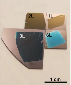
Figure 1.3. Transferred different layer MoS2 film onto SiO2/Si substrate ...4
Figure 1.4. Absorption efficiency of monolayer suspended MoS2 in visible light range .... ...5
Figure 1.5. Calculated band structures of (a) bulk MoS2, (b) quad-trilayer MoS2, (c) bilayer MoS2, and (d) monolayer MoS2.[5] ...6
Figure 1.6. Illustration of exciton recombination process ...6
Figure 1.7. Illustration of exciton-exciton annihilation process ...7
Figure 1.8. Raman spectrums of MoS2 film with different layer number (a). The illustration of phonon vibration modes of MoS2 (b) [24] ...9
Figure 2.1. The AFM measurement of MoS2 film with different layer number ...13
Figure 2.2. The ellipsometry measurement fitted results for delta and phi of MoS2 film with different layer number ...14
Figure 2.3. Anomalous layer-dependence of the dielectric function of 2D MoS2 ...16
Figure 2.4. Independence of the measured dielectric function from synthetic processes and substrates (a). Measured and simulated reflection spectra of monolayer MoS2 on different substrates, sapphire and silicon with 80 nm thick thermal oxide (b) ...17
Figure 2.5. Stability of the dielectric function ...18
Figure 2.6. Comparison of the measured and calculated dielectric function of 2D MoS2 ... ...22
Figure 2.7. Strong, layer-dependent excitonic effects in atomically thin MoS2 films ...23
Figure 2.8. Geometric confinement of excitons in MoS2 films ...27
Figure 3.1. Gated refelction and refractive index of monolayer WS2 ...32
Figure 3.2. Gated refelction of monolayer WS2 around C exciton ...32
Figure 3.3. Gated refelction of monolayer MoS2 and WSe2 ...33
Figure 3.4. Fitted and measured spectra reflection of monolayer WS2 under different gate voltages ...35
Figure 3.5. Photoluminescence spectra of monolayer WS2 under different gate voltages (a). I-V curve measurement of monolayer WS2 (b) ... 36
Figure 3.6. Fitted real and imaginary parts of dielectric function under different gate voltages ...37
Figure 3.7. Tunability of physical parameters in monolayer WS2 ...38
Figure 3.8. Bandgap renormalization and change in exciton binding energy in monolayer WS2 ...39
Figure 3.9. Change in the binding energy of charged A exciton as a function of the gating voltage ...41
Figure 4.1. PL efficiencies of (a) suspended monolayer WS2, (b) suspended monolayer MoS2, (c) as-grown monolayer WS2 on sapphire substrates, and (d) as-grown monolayer
MoS2 on sapphire substrates as a function of the incident power density ...49
Figure 4.2. Optical image of typical as-grown monolayers on sapphire substrates and transferred monolayers on SiO2/Si substrates pre-patterned with holes ...49
Figure 4.3. Dependence of the PL spectra of suspended MoS2 and WS2 on incident power ... ...50
Figure 4.4. Differential reflection of suspended WS2 with different pumping fluences ..52
Figure 4.5. Differential reflection of suspended MoS2 with different pumping fluences .52 Figure 4.6. Differential reflection of supported MoS2 at different temperatures ...53
Figure 4.7. Differential reflection of supported WS2 with different pumping fluences ...54
Figure 4.8. Differential reflection of supported MoS2 with different pumping fluences ..55
Figure 4.9. (ΔR/R)0/(ΔR/R)t -1 of (a) as-grown MoS2 and (b) as-grown WS2 ...55
Figure 4.10. Measured refractive index of monolayer WS2.(a) measured real and imaginary part of the refractive index of monolayer WS2. (b) measured and fitted transmission of as-grown monolayer WS2 on sapphire substrates ...57
Figure 4.11. Measured refractive index of monolayer WS2.(a) measured real and imaginary part of the refractive index of monolayer WS2. (b) measured and fitted transmission of as-grown monolayer WS2 on sapphire substrates ...61
Figure 5.1. Improved luminescence efficiency of suspended monolayers WS2 and MoS2 . ...65
Figure 5.2. Improved luminescence efficiency of suspended monolayer WSe2 ...66
Figure 5.3. Raman and PL mapping of as-grown MoS2 on sapphire substrates ...67
Figure 5.4. Raman and PL mapping for the monolayer MoS2 transferred on sapphire substrates ...68
Figure 5.5. Effect of the transfer process on the Raman spectrum ...69
Figure 5.6. Effect of the transfer process on the PL efficiency ...70
Figure 5.7. Effect of trapped water moisture on the PL efficiency of monolayer MoS2 and WS2 ...71
Figure 5.8. Heavy n-doping in the monolayer transferred onto hydrophilic substrates ....72
Figure 5.9. Absence of heavy n-doping in the monolayer transferred onto hydrophobic substrates ...73
Figure 5.10. PL spectra of the monolayer MoS2 directly grown on mica substrates and the monolayer transferred onto mica substrates. ... 74
Figure 5.11. Doping effect of the substrate ...77
Figure 5.12. Fitting of the PL emission of monolayer MoS2 on different substrates ...78
Figure 5.13. Calculated charge transfers between monolayer MoS2 and various substrates ...80
Figure 5.14. PL and Raman of the monolayer MoS2 grown on different substrates ...83
Figure 5.15. Comparable crystalline quality in the monolayer MoS2 grown on different substrates ...84
Figure 5.16. Substrate-dependent PL of supported monolayer WS2 ...84
Figure 5.17. Raman and PL of monolayer WSe2 on different substrates ...85
Figure 5.18. Defect-assisted recombination in as-grown monolayer MoS2. ... 88
Figure 5.20. Normalized PL collected from the two different areas of as grown WS2. ...90
Figure 5.21. Similar exciton dynamics in suspended monolayers with different sizes. ...91
Figure 5.22. Effect of the substrate on radiative decay. ...92
CHAPT 1: Introduction and background
1.1 Introduction
Atomically thin two dimensional transition metal dichalcogenide materials (TMDC) has
attracted lots of attention from researchers in recent years since it is discovered [1]. This
monolayer TMDC family shares some similarities with graphene. They are both composed of
one single atomic layer with hexagonal arrangement of atoms crystal structures. The
interaction between different layers for both TMDC and graphite is only Van der Waals force,
makes the surface passivated without dangling bonds.
Figure 1.1. MX2 structure with (a) top view [2] and (b) side view.
They both have strong mechanical strength that can apply to elastic devices [3, 4]. The key
difference between TMDC and graphene is that the TMDC is semiconductor material
functional optoelectronic devices those requires good on and off switch. However for TMDC,
they have band-gaps range from 1.6ev to 2.1ev depend on their composition and layer
numbers[5, 6]. Though the mobility of TMDC is not as good as graphene, The TMDC still
can reach to high mobility [7, 8]. All of these electronic properties make TMDC a very
promising candidate that can lead to real next generation atomically thin devices era. What’s
more important, the TMDC has very novel optical properties. Their band-gap is located in
visible light region, and with extremely strong light-matter interaction even with single layer
material due to its strong excitonic effect. It will be the main topic I will discuss in this thesis.
The TMDC material can change from indirect band gap material to direct band gap material
when thickness reduces to monolayer. Very high luminescence efficiency has been observed
for monolayer TMDC [9, 10]. Efficient TMDC based LED has been realized [11, 12]. People
even successfully make out laser based on this monolayer TMDC [13, 14]. Overall, the
extraordinary optical and electronic properties of 2D TMDC make it great material to realize
next generation atomically thin optoelectronic devices.
1.2 Strong excitonic effect of 2D TMDC
Excitons are coupled electron-hole pairs via coulomb attraction. The distinct optical
properties of 2D TMDC are originating from the strong excitonic effect of the material. Since
it is atomically thin layered materials with very small Bohr radius, so the dielectric screening
effect for exciton is very small. It leads to very large exciton binding energy. The simplified
Figure 1.2. Exciton in monolayer MX2. The interaction of electron-hole pair can go out of the material reduces the dielectric screening effect, generating strong binding energy.
For conventional bulk semiconductors or semiconductor quantum wells, the exciton binding
energy is smaller than 100mev. However for monolayer TMDC such as monolayer MoS2,
WS2, WSe2, their exciton binding energy are of one order higher magnitude range from
400mev to 800mev [15-21]. The strong binding energy also results in very strong
many-body interactions for this low dimension material. For instance, the charged exciton called
trion, which is one extra carrier bound to a neutral exciton form a three body complex, can be
observed at room temperature in TMDC. But for conventional semiconductors, trion can only
observed at low temperature region. I will show later in the thesis that this trion has profound
effect on the optical properties of 2D TMDC. Moreover, not only strong three-body effect
exist, even higher order interaction like exciton-exciton interaction also play very important
role in the light emission efficiency of monolayer TMDC. We will also discuss this in
Chapter 4. In fundamental wise, the 2D TMDC really provide a perfect platform to observing,
studying the many-body interaction, which has been the most important topic in condensed
matter physics. In engineering wise, the exciton involved many-body interaction can be
tuned by electric field. And many-body interaction is intrinsically affected by the density of
excited excitons which is determined by excitation power. These indicate possibility to
This thesis will address to answer two questions: How the strong exciton many body effects
affect the optical properties of 2D TMDC? How to engineering the excitonic effects to
improve the optical performance of 2D TMDC?
1.3 Light-matter interaction of 2D TMDC
There are two main processes for light-matter interaction of 2D TMDCs, which are also two
key processes relate to application of 2D TMDCs in photonic devices. One is the light
absorption, reflection and transmission process. Another one is the light emission process.
The light absorption/reflection/transmission process is dominated by the optical dielectric
function of the 2D TMDCs. Even for a single layer TMDCs, it can have very strong
absorption and reflection efficiency to the light.
light. Monolayer MoS2 has been proved to have 5% solar absorption [23]. These are due to
strong quantum confinement effect and weak screening effect of the excitons when the layer
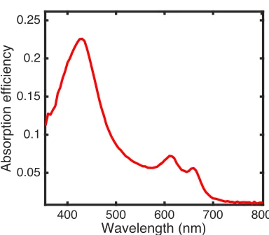
thickness reduces to a few atoms thickness. Fig. 1.4 shows the absorption efficiency
spectrum of the single suspended MoS2 layer, it can absorb over 20% of light around
430nm(C exciton peak) and 7% of light in range 600nm to 680nm (A exciton and B exciton
peaks). This makes atomically thin layer 2D TMDCs potentially a very good platform to
realize functional nanophotonic devices such as ultrathin optical modulator, solar absorber
and phase steering meta-surfaces.
Figure 1.4. Absorption efficiency of monolayer suspended MoS2 in visible light range.
The quantum efficiency is most important property of light emission. Enhancing the light
emission efficiency is the key to use the material to realize application like LED and Laser.
For the 2D TMDCs, the monolayer TMDCs are direct band gap material while the
multi-layer TMDCs are indirect band gap material Fig. 1.5. Only the monomulti-layer TMDCs promised
to high light emission efficiency.
400 500 600 700 800
Wavelength (nm) 0.05
0.1 0.15 0.2 0.25
Figure 1.5. Calculated band structures of (a) bulk MoS2, (b) quad- rilayer MoS2, (c) bilayer MoS2, and (d) monolayer MoS2. The solid arrows indicate the lowest energy transitions. [5]
So we will only focus our discussion on monolayer light emission. The light emission
process is determined by the recombination process of excited excitons (Fig 1.6). The
efficiency is determined by the competition between the radiative recombination rate and
non-radiative recombination rate. To enhance the light emission efficiency is about to
The radiative recombination rate is determined by radiative lifetime of exciton k r =1/τr. Same
to the non-radiative lifetime knr=1/τnr. The radiative lifetime of exciton is mostly determined
by the intrinsic properties of the material that only relate with the exciton binding energy and
band structure. The non-radiative lifetime however is affected by extrinsic properties, such as
defects, impurities, doping level and substrate conditions.
Figure 1.7. Illustration of exciton-exciton annihilation process.
Due to the strong exciton binding energy of monolayer TMDCs, strong many-body
interaction caused nonlinear higher order recombination term like exciton-exciton
annihilation Fig. 1.7 will also play a very important role, which we will discuss in detail in
Chapter 3.
1.4 Experimental methods
There are several important optical spectroscopy methods to characterize the low
dimensional TMDCs. There are two categories of the optical characterize methods, one is
time averaged spectroscopy and another one is time resolved spectroscopy. The time average
reflection/transmission spectroscopy and Raman spectroscopy. These measurements have
time scale much longer than the material response time, so the measurements are detecting
the physical response from steady states. This kind of characterization not only tells
information of fundamental properties of the material but also reveals how good is the optical
performance of the material that directly relate to the device performance. In addition, the
Raman spectroscopy is very useful tool to identify the layer number of TMDC which is
pretty difficult for other techniques. Even atomic force microscopy sometimes cannot get
precise layer number when thickness goes down to below 1nm to 2nm scale. The Raman
spectroscopy essentially detects the inelastic electron-phonon scattering signal so as to show
the phonon modes properties. Take MoS2 film as an example. There are two signature
phonon modes in the range from 350cm-1 to 450cm-1. One is in plane optical phonon mode
E12g, another is out of plane mode A1g (Fig 1.8). As the layer number increases, the A1g
vibration mode will be compressed that lead to blue shift of the Raman shift of A1g peak.
Meanwhile, for the in plane E12g mode, increasing layer number will results in larger
dielectric screening. It will soften the E12g vibration mode which cause redshift to E12g. This
will give us the layer dependent Raman spectrum like showing in Fig 1.8 Generally, the
Raman shift difference between A1g and E12g peaks can precisely determine the layer
numbers, for monolayer the difference is range from 19cm-1 to 20cm-1; bilayer is 22cm-1 to
Figure 1.8. (a) Raman spectrums of MoS2 film with different layer number. (b) The
illustration of phonon vibration modes of MoS2 [24].
For the time resolved spectroscopy, this kind of measurement can resolve the physical
response of the material in a very short time scale before the system reach to steady state.
The time resolved spectroscopy provide perfect way to detect the dynamics of the carriers
and excitons, which is very important to understand the fundamental physics process that
affect the optical performance. In this thesis, the main time resolve spectroscopy technique
been used is pump probe transient absorption spectroscopy. The carriers in the material have
been pumped to excited states a short pulse laser (150fs) with photon energy larger than the
band gap (2.1ev), and a time-delayed probe pulse beam with photon energy around the band
edge (1.88ev for MoS2, 2ev for WS2 and 1.76v for WSe2) is used for detect the differential
reflection (ΔR/R). ΔR is the reflection difference between with pump and without pump.
After the system has been pumped, the conduction (valence) band has been occupied by the
pumped. That will be indicated by change in reflection also. The excited excitons will
recombined after ps or ns scale, the change in reflection of probe beam would be able to tell
the population of excitons in the excited states in time range from 0ps to 500ps. So the
CHAPT 2: Exciton dominated dielectric function of atomically thin MoS2 films
We systematically measure the dielectric function of atomically thin MoS2 films with
different layer numbers and demonstrate that excitonic effects play a dominant role in the
dielectric function when the films are less than 5-7 layers thick. The dielectric function
shows an anomalous dependence on the layer number. It decreases with the layer number
increasing when the films are less than 5-7 layers thick but turns to increase with the layer
number for thicker films. We show that this is because the excitonic effect is very strong in
the thin MoS2 films and its contribution to the dielectric function may dominate over the
contribution of the band structure. We also extract the value of layer-dependent exciton
binding energy and Bohr radius in the films by fitting the experimental results with an
intuitive model. The dominance of excitonic effects is in stark contrast with what reported at
conventional materials whose dielectric functions are usually dictated by band structures. The
knowledge of the dielectric function may enable capabilities to engineer the light-matter
interactions of atomically thin MoS2 films for the development of novel photonic devices,
such as meta-surface, waveguides, light absorbers, and light emitters.
2.1 Introduction
Two-dimensional (2D) transition metal dichalcogenide (TMDC) materials have been known
exhibiting strong exciton binding energy that may be one order of magnitude larger than
conventional semiconductor materials[1, 25-29]. However, how the extraordinarily strong
exciton binding energy could affect the light-matter interactions such as dielectric functions
of the materials has remained unexplored. The lack of knowledge about the dielectric
photonic fields such as metamaterials[30], which relies on the sophisticated manipulation of
effective dielectric functions to enable novel optical functionalities. In this work we have
measured the dielectric function of atomically thin MoS2 films and discovered that it is
dominated by the effect of the tightly bound excitons, as evidenced by an anomalous
dependence of the dielectric function on the layer number. The dielectric function decreases
with the layer number increasing when the MoS2 films are less than 5 layers thick, but turn to
increase with the layer number for thicker. We also quantitatively evaluate the exciton
binding energy and Bohr radius of the thin films by fitting the experimental results with an
intuitive model. The observed dominance of excitonic effects in the dielectric function is in
stark contrast with what expected at conventional materials, whose dielectric functions are
usually dictated by band structures[31, 32]. Our success in this discovery is built upon a
unique self-limiting chemical vapor deposition (CVD) process that we have recently
developed[33]. The self-limiting CVD process can be used to grow centimeter-scale,
uniform, and high quality atomically thin MoS2 films with controlled layer numbers and
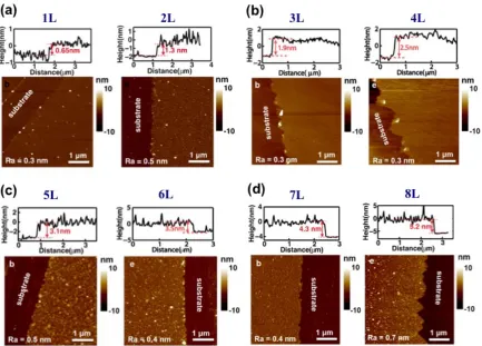
remarkable uniformity (Fig. 2.1). This allows us to examine the dielectric function of MoS2
films as a function of well-defined layer numbers. Our work is different from earlier
research for the dielectric function of MoS2 films[34, 35], whose results are likely inaccurate
due to the lack of satisfactory uniformity or precise control of the layer number.
2.2 Measurement of layer-dependence of the dielectric function
We measured the dielectric function (ε1 +iε2) of as-grown MoS2 films on sapphire substrates
the dielectric function in the visible range that are derived from experimental measurements
(see Fig2.2 for the fit between experimental and simulated results).
Owing to the extreme geometrical anisotropy of the film, what we obtained is actually the
in-plane component of the dielectric tensor because the out-of-in-plane dielectric function may
only contribute trivially to the optical response due to the difficulty in exciting the vertical
dipole of the atomically thin film[36]. As further evidence for the measured in-plane
dielectric function, we performed the spectroscopic ellipsometry at different incident angles
(40°-75°), and all of them ended up with giving very similar dielectric functions. The
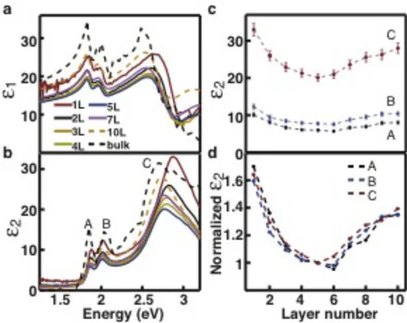
Figure 2.3. Anomalous layer-dependence of the dielectric function of 2D MoS2. (a-b) Real and imaginary parts of the dielectric function of 2D MoS2 vs. layer number. Also given is the dielectric function of bulk MoS2. The three peaks can be assigned to A, B, and C excitons as labeled. (c) The dependence of the imaginary part ε2 of the dielectric function at the A, B, and
C peaks on layer number. The error bar is 5% and estimated from the measurement results of multiple samples. (d) Normalized ε2 at the A, B, and C peaks vs. layer number. The normalization is performed with respect to the corresponding value of each peak in the 5-layer MoS2. Error bar is ignored for visual convenience.
The three peaks in the spectral dielectric function can be assigned to A, B, and C from low to
high energies, respectively[20, 38-40]. The A and B peaks are related with the transition
from the spin-orbit split valence bands to the lowest conduction band at the K and K’ points,
while the C peak is associated with the transition from the valence band to the conduction
Figure 2.4. Independence of the measured dielectric function from synthetic processes and substrates. (a) Measured dielectric constants of as-grown monolayer MoS2 made by two different CVD processes, one using MoCl5 and S as the precursors and the other using MoO3 and S as the precursors. The growth substrate in both growths is sapphire. (b) Measured and simulated reflection spectra of monolayer MoS2 on different substrates, sapphire and silicon with 80 nm thick thermal oxide. The monolayer MoS2 involved is grown on sapphire substrates and then transferred to SiO2/Si substrates. The simulation uses the optical constant measured with the as- grown MoS2 on sapphire substrates.
The measured dielectric function is not sensitive to the synthetic process or the substrate. The
dielectric functions measured from the MoS2 grown by using MoCl5 and S as the
precursors[33] and by using MoO3 and S as the precursors[41] are essentially identical (Fig
2.4a). We also find that the dielectric functions of the as-grown MoS2 films on sapphire
substrates and those transferred onto SiO2/Si substrates are identical (Fig 2.4b). Additionally,
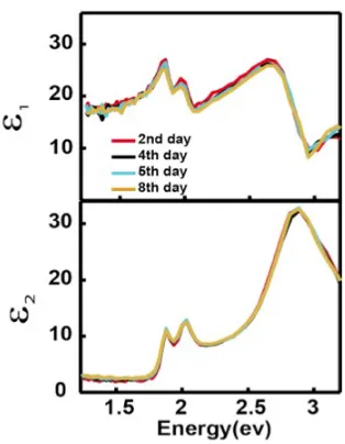
Figure 2.5. Stability of the dielectric function. Real (upper panel) and imaginary (lower panel) parts of the dielectric function of monolayer MoS2 measured at different times after synthesis.
We monitored the dielectric function of the as-grown MoS2 films on sapphire substrates as a
function of the time for the films to be exposed to ambient environment. We monitored the
dielectric function of the films exposed to ambient environment for more than one week and
found no change in the measured result (Fig. 2.5). The result we measured for the monolayer
MoS2 film is consistent with what previously measured using spectroscopic ellipsometry20
but is 10-15% less than the results derived from absorption spectra[42, 43]. We do like to
point out some difference in the spectroscopic ellipsometry used by us as well as Ref.42 and
the spectroscopic absorption technique used in Ref.43. Spectroscopic ellipsometry is the
most established technique for the measurement of dielectric functions, in which two
parameters are measured at each wavelength and the dielectric function can be uniquely
determined in any spectrum range with the thickness information of the film indepedently
determined by AFM. The dielectric function may be derived from spectroscopic reflection
function using the Kramer-Kronig relationship requires information of the absorption in the
entire spectral range. In Ref.43 the absorption of the monolayer in the range higher than 3 eV,
whose value is not experimentally available, is assumed to be equal to that of the bulk
counterpart. This assumption might overestimate the dielectric function to some degree. We
believe this is likely the reason why our result is around 10-15% less than the result reported
in Ref.43.
Significantly, the measured dielectric function shows an anomalous dependence on the layer
number (Fig 2.3). It decreases with the layer number increasing when the film is less than
5-7 layers thick and then turns to increase with the layer for thicker films. We were very careful
to ensure no artifact introduced in the measurement. More specifically, we performed
extensive AFM for each of the films studied prior to the ellipsometry measurement and
confirmed the atomic-scale smoothness (roughness usually < 0.5 nm except the 8L, 9L and
10L films, whose roughness is a little bit larger in the range of 0.7-0.9 nm, see Fig 2.1) and
excellent uniformity of the film. Additionally, for the result of each layer number, we
measured at least three different sets of samples and observed only minor variation (5%) in
the resulting dielectric function. To further illustrate this anomalous layer-dependence, we
extract the imaginary part of the dielectric functions at the A, B, and C peaks from Fig. 2.3b
and plot it as a function of the layer number (Fig.2.3c). The result clearly shows a decrease
and then an increase in the dielectric function with the layer number continuously increasing
from one. The layer dependence is similar for all the A, B, and C peaks (Fig. 2.3d). Given
the similarity in the layer dependence, we only focus on the C peak in the following
2.3 Strong excitonic effect on layer dependent dielectric function
To obtain physical insights into the observed layer dependence, we examine the dielectric
function from the perspective of quantum mechanics. We only focus on the imaginary part ε2
because the real part ε1 can be deterministically correlated to ε2 by the well-established
Kramer-Kronig equation[44]. Fundamentally, ε2 is related with interband transitions as[31, 44,
45]
(2.3.1)
where ω is the frequency, ħis the Planck’s constant, e and m0 are the charge and mass of free
electrons, Jcv is the joint density of the initial (valence band) and final (conduction band)
states involved in the transition. pcv is an optical matrix element indicating the probability of
the transition from the initial to final states. It consists of an integral over a unit cell that
involves the momentum operator as well as the unit cell wavefunctions in the conduction and
valence bands. represents the effect of excitons on the oscillator strength of the
interband transition, where U is the relative motion wavefunction of the eletrons and holes
bound by Coulomb interactions and 0 indicates the physical overlap of the electron and hole
wavefunctions. Ecv is the optical energy gap between the conduction and valence bands
involved and Γ is a damping constant determining the bandwidth of the interband transition.
For simplicity, we only focus on the dielectric function at the peak position (on-resonance) as
shown in Fig. 2.3c-d, where Ecv - ħω = 0 and Eq.(2.3.1) can be simplified as
(2.3.2)
ε2
( )
ω =4π2e2 m0
2ω2 Jcv pcv
2
U(0)2 Γ/ 2
Ecv−!ω
(
)
2+
(
Γ/ 2)
2U(0)2
ε2(ω)= 4π
2
e2
m02ω2 Jcv pcv
2
U(0)2 2
Physically, Γ represents the width of the peak. From Fig. 1b the peak can be found
phenomenally remaining to be similar in the films with different layer numbers. Therefore, it
is reasonable to consider that Γ is independent of the layer number. The optical matrix
element pcv is also independent of the layer number because it is only related with unit cells
and unit cell wavefunctions, both of which are not dependent on the layer number. The
independence of pcv on geometrical features has previously been demonstrated at quantum
wells[46]. Therefore, Eq. (2.3.2) can be further simplified as
(2.3.3)
where A0 includes all the terms independent of the layer number. Eq. (2.3.3) indicates that
the layer dependence of the dielectric function may result from only two parameters: the joint
density of states Jcv and the excitonic effect .
Figure 2.6. Comparison of the measured and calculated dielectric function of 2D MoS2. (a) Calculated imaginary part ε2 of the dielectric function of MoS2 with different thickness. (b) Comparison of experimental and calculated results for ε2 at the C peak as a function of the layer number. The error bar in the experimental result is ignored for visual convenience.
ε2(ω)=A0JcvU(0)
2
U(0)2
2 4 6 8 10
10 15 20 25 30 35 Layer number
1.5 2 2.5 3
0 5 10 15 20 Energy(eV)
ε
2ε
2We can get more insight by further examining the specific layer dependence of the two
parameters Jcv and . The joint density of states Jcv is determined by the band structure
and expected to monotonically increase with the layer number. This is because the density of
states in 2D materials is well known to be smaller than that in 3D materials[31, 44] and the
increase of the layer number in effect enables a continuous evolution from two dimensions
(monolayers) to three dimensions (bulk). To quantitatively elucidate the layer dependence of
Jcv, we calculate the ε2 of MoS2 films using density functional theory (DFT) techniques
without considering excitonic effects[20]. The calculation result is given in Fig. 2.6a and
essentially represents the density of states Jcv. It reproduces the major spectral features of the
experimental results and indeed shows a monotonic increase with the layer number. For the
convenience of comparison, we plot the calculated and measured dielectric functions at the C
peak as a function of the layer number in Fig. 2.6b. The calculated results are
understandably smaller than the experimental results due to the exclusion of excitonic effects.
Of our interest is to compare the layer dependence in the calculated and experimental results.
The similarity of the two results for the films > 5L suggests that the observed
layer-dependent increase in the dielectric function in the relatively thicker films may be correlated
to the effect of the density of states Jcv. However, for the films less than 5 layers thick the
calculated layer-dependence is opposite to the experimental observation (Fig. 2.6b). This can
be correlated to the other parameter not considered in the calculation, the excitonic effect
. The excitonic effect is expected to be strong and to quickly decrease with the layer
number due to the well known layer-dependent exponential decrease of exciton binding
energy[38].
U(0)2
Figure 2.7. Strong, layer-dependent excitonic effects in atomically thin MoS2 films. (a) The
position of the C peak in MoS2 films as a function of the thickness of the film L. The error
bar ±0.005 eV results from the possible errors in determining the peak position. The dashed
lines are the fitting results using the model of infinite quantum wells (fitting 1) and the
quantum well in fraction space (fitting 2) (b) The position of the C peak in MoS2 films as a
function of 1/L2, where L is the thickness of the film. The red line is the fitting results using
the model of infinite quantum well with the fitting equation given as shown. The inset is a
magnified version of the area indicated by the dashed yellow rectangle. (c) The dependence
of the binding energy and exciton radius in MoS2 films on the layer number.
The layer-dependent excitonic effect can be understood more quantitatively by examining the
excitonic peak position with an intuitive model that involves quantum confinement and
exciton binding energy. Of our interest is to quantitatively evaluate the layer dependence of
the exciton binding energy from the observed evolution of the C exciton peak position with
the layer number (Fig. 2.7a). The excitonic peak position (i.e. optical bandgap) is equal to
the electronic bandgap minus the exciton binding energy, and its layer dependence originates
from the layer dependence of both components. Should the layer dependence of the
20 40 60
2.7 2.75 2.8 2.85 2.9
0 0.01 0.02 0.03 2.7
2.75 2.8 2.85 2.9
0 2 4 6x10⁻⁴
2.74 2.78
Peak
position
(eV)
Thickness L (Å) fitting 1 fitting 2
0
1/L2 (Å-2)
Peak position (eV) a b 2.695+150.9/L2 0.1 0.2 0.3 0.4 Binding
energy
(eV)
2 4 6 8 10
to experimentally or theoretically evaluate the electronic bandgap of MoS2 with different
layer numbers. However, we find out that the layer dependence of the electronic bandgap
may be reasonably correlated to quantum confinement effects. The peak position of the C
exciton EC in the films thicker than 7 layers shows a linear dependence on 1/L2 (Fig. 2.7b),
and can be fitted by the conventional model of infinite quantum wells as EC = Eg + Ry +
π2ħ2/2meffL2 – Ry. where Eg is the position (optical bandgap) of the C peak in bulk MoS2
materials (Eg = 2.695 eV as measured in Fig. 2.3b), Ry is the exciton binding energy and
assumed not changing with the thickness in the model of infinite quantum wells, and meff is
the reduced electron-hole effective mass of the film. The introduction of Ry in the equation is
to illustrate that the optical bandgap is equal to the electronic bandgap (the first three terms)
minus the exciton binding energy (the last term). The fitting to the experimental results (the
red lines in Fig. 2.7a-b) gives EC = 2.695 eV + 150.9/L2, from which we can derive the
reduced effective mass meff = 0.250 m0 for the C extions in bulk MoS2 and the films thicker
than 7 layers. We can also derive the exciton binding energy Ry = 58.9 meV and Bohr radius
ab = 1.61 nm in bulk MoS2 and thick films, in which the static dielectric constant is set to be
7.6 as measured for bulk MoS2 previously[47].
The peak position EC in the films thinner than 5-7 layers shows apparent deviation from the
model of infinite quantum wells (Fig. 2.7b). Instead, we can fit the experimental results with
a model of quantum wells in fractional dimensional space as[48, 49]
(2.3.4)
where D is the effective dimensionality that is defined by the ratio of the exciton binding
energy Ry* in the films and that of bulk MoS2 Ry as [(D-1)/2]2 = Ry/ Ry*. Again, the first
EC =Eg+Ry+
π2!2
2meffL
2 ⎡⎣
(
D−1)
/ 2⎤⎦ 2− Ry
D−1
(
)
/ 2three terms of eq. (4) represent the electronic bandgap and the last term indicates the exciton
binding energy. The factor of [(D-1)/2]2 in the third term originates from the change in the
effective mass associated with the effective dimensionality. For the films thicker than 7
layers, D is 3 and Eq. (2.3.4) is then reduced to the equation for infinite quantum wells. By
fitting the experimental results with Eq. (2.3.4), we can have the effective dimensionality D
as 1.75, 2.07, 2.30, 2.51, 2.65, and 2.83 for the films in layer number of 1, 2, 3, 4, 5, and 6,
respectively. We can then derive the corresponding exciton binding energies using Ry* =
Ry/[(D-1)/2]2 as 0.421eV, 0.206 eV, 0.139 eV, 0.103 eV, 0.0865 eV, and 0.0704 eV; we can
also derive the corresponding Bohr radius of excitons from ab*= ab(D-1)/2[48, 49] as 0.602
nm, 0.861 nm, 1.04 nm,1.22 nm,1.33 nm, and 1.47 nm, respectively. These results are
plotted in Fig. 2.7c.
The model we used to fit the experimental result is based on an assumption that the layer
dependence of the electronic bandgap can be ascribed to the effect of quantum confinement.
This is supported by our experimental results, in particular, the consistence between the
observed peak position of the films thicker than 7 layers and what predicted from the model
of infinite quantum wells. However, more theoretical and experimental studies would be
necessary to provide more rigorous support, which is to our best knowledge expected to very
difficult. Nevertheless, the result we obtained by fitting the experimental results using this
model seems to be reasonable when compared to the limited number of studies on the exciton
binding eerngy and Bohr radisu available in the literature. There is not study that would
allow us to systematically crosscheck all of our results. For instance, the binding energy Ry =
exciton in bulk MoS2, which are 87.2 meV and 1.11 nm, respectively[50]. Additionally, the
Bohr radius (0.602 nm) we derived for the C exciton in monolayer MoS2 nicely matches the
theoretical prediction, ~ 0.5 nm[40]. The derived binding energy (0.421 eV) is reasonable
compared with what reported for the A exciton, which is believed to be 0.4-0.6 eV in
monolayer MoS2 [20, 21].
With the information of the exciton binding energy and radius, the observed layer
dependence of the dielectric function can be intuitively understood from a perspective of
geometric confinement. Fig. 2.8 shows the comparison between the size of excitons and the
thickness of the film. While the film is highly anisotropic, the size of the exciton is
schematically illustrated by the diameter of a sphere anyway. This is because Eq. (2.3.4),
which we used to derive the exciton radius, treats the excitons as spheres in an isotropic
space by converting the geometrical anisotropy into fractional dimensionality[48, 49]. The
size of the exciton in bulk MoS2, 3.22 nm, is close to the thickness of the 5L film, 3.10 nm
(Fig. 2.8a). Therefore, the exciton in MoS2 films is expected to start experiencing substantial
geometrical confinement when the layer number of the film is decreased to 5, which may
lead to decrease in the exciton size. Intuitively, a smaller exciton radius can better facilitate
the spatial overlap of the electron and hole wavefunctions and subsequently cause larger
amplitude in . The layer-dependent decrease of the dielectric function is expected when
the dependent decrease of the excitonic effect offsets or even exceeds the
layer-dependent increase of the join density of states.
Figure 2.8. Geometric confinement of excitons in MoS2 films.(a) Comparison of the size of the exciton in bulk MoS2 with the thickness of MoS2 films. The regime where the film is thinner than the exciton size is categorized as strong confinement. (b-e) Schematic illustration of the size of excitons in the films with different layer numbers.
The main conclusion we draw from the analysis of the C exciton, i.e. the dominance of
excitonic effects in the dielectric function, can be applied to the A and B excitons as well due
to the similar layer dependence in corresponding dielectric functions (Fig 2.3c-d). However,
it is difficult to quantitatively extract the binding energy and Bohr radius for the A and B
excitons as what we did for the C exciton. This is because that the positions of the A and B
excitons do not show substantial layer dependence as what observed as the C exciton, which
makes the fitting by the intuitive model difficult. One reason for the less layer dependence
observed at the A and B excitons could be related with the random variation of the position of
the A and B excitons due to local doping effect from the substrate, which may be as large as ~
10 meV [51]. Another reason could be related with the better localization of the A and B
2.4 Conclusion
While our work mainly focuses on MoS2, we believe that similar dominance of excitonic
effects in the dielectric function could generally exist in all the atomically thin
semiconducting TMDC materials. Our result bears significant implications for the
development of photonics devices with 2D TMDC materials. The obtained dielectric
function and refractive index for the MoS2 with different layer numbers can be immediately
useful for the rational design of photonic devices. In particular, as excitons are subject to
influence of electric or magnetic fields, the dominance of excitonic effects in the dielectric
function makes atomically MoS2 films an unprecedented platform that may enable the
development of field-effect photonics, whose optical functionalities would be tuned by
CHAPT 3: Giant gating tunability in refractive index of transition metal dichalcogenide monolayers
We report that the refractive index of transition metal dichacolgenide (TMDC) monolayers,
such as MoS2, WS2, and WSe2, can be substantially tuned by up to 60% using
CMOS-compatible electrical gating. This strong tunablility is rooted in the strong excitonic effect of
the monolayers and the high susceptibility of the excitons to the influence of free charge
carriers. More specifically, we have elucidated that the tunability mainly results from the
effects of free charge carriers on spectral broadening and the inter-transfer of transition
probabilities between neutral and charged excitons, while the other effects of free charge
carriers, including bandgap renormalization and change of exciton binding energy, only play
negligible roles. The electrical gating of refractive index may open up a new age of
field-effect photonics in which the optical functionality can be dynamically controlled in speed
comparable to that of state-of-art CMOS circuits.
3.1 Introduction
Electrically gating photons in ways comparable to the gating of electrons has the potential to
revolutionize the photonic industry. It would enable the development of unprecedented
dynamic photonics with operation speed comparable to that of state-of-art CMOS circuits. It
would also enable chip-scale integration of optical functions into electronic circuits, which
could dramatically improve the computing speed [52, 53]. However, the electrical gating of
photons is very challenging because of the difficulty in gating refractive index. Photon is
transmission, absorptions, and scattering. As refractive index consists of the most
fundamental measure for light-matter interactions, to gate photons is in essence to gate
refractive index. None of the existing approaches for electrically gating refractive index may
provide satisfactory tunability, tuning spectral range, speed, and compatibility with CMOS
circuits. The most common strategy to electrically tune refractive index relies on the plasma
dispersion effect of free charge carriers, in which the optical absorption of injected electrons
or holes may give rise to changes in the refractive index.[54-61] But the density of the charge
carriers that can be injected is limited, and this fundamentally limits the tunability in
refractive index, usually in the scale of 0.1-1%.[54-58] While ionic gating has been recently
reported to be able to enable larger tunability,[62-64] its nonlocal nature, inferior chemical
stability, and intrinsically slow switching make it not ideal in terms of speed and
compatibility with CMOS circuits.
Here we demonstrate that the refractive index of monolayer transition metal dichalcogenide
(TMDC) materials, including MoS2, WS2, and WSe2, can be substantially tuned by up to
60% using CMOS-compatible gating. Unlike the previous approach of relying on the plasma
dispersion effect of free charge carriers to tune the refractive index,[54-58] this large
tunability in refractive index is rooted in the strong excitonic effects of the monolayers [65]
and the high susceptibility of excitons to the influence of free charge carriers. More
specifically, we have discovered that the tunability is mainly due to the effects of free charge
carriers in spectral broadening and the inter-transfer of transition probabilities between the
neutral and charged excitons, while the other effects, including bandgap renormalization and
change in exciton binding energy, play only negligible roles. It is worthwhile to point out that
monolayer TMDC materials [66-71], but this work is the first ever quantitatively
demonstrating the gated tunability in refractive index as well as the dominating mechanism.
3.2 Analysis of gating refractive index
We start with examining the spectral reflection of TMDC monolayers. Figure 1a inset
schematically illustrates the measurement configuration. The monolayers are grown on
degenerately doped Si substrates with thermally grown silicon oxide (SiO2/Si) using well
established chemical vapor deposition (CVD) processes.[72, 73] The source and drain
electrodes are fabricated on top of the monolayer using standard e-beam lithography and
metallization procedures. We have confirmed that the electrodes form Ohmic contact with
the monolayers. In the experiments, the Si substrate is used as the gate and the potentials at
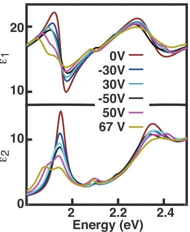
the source and drain electrodes are kept to be the same. Fig 3.1a shows the spectral reflection
Figure 3.1. Gated refelction and refractive index of monolayer WS2. (a) Reflection spectra of monolayer WS2 at different gating voltages. The inset is schematic illustration for the measurement configuration. The two arrows point out the two excited states of the A exciton, 2S and 3S. (b) Fitted real part n and imaginary part k of refractive index with different gating voltages. (c) The peak value of the real part (at around 1.92 eV) and the imaginary part (at around 1.95 eV) as a function of carrier densities.
The reflection of the A exciton shows substantial variation with the gating voltage, while the
variation is much less at the B exciton and essentially negligible at the C exciton (Fig. 3.2).
Figure 3.2 Gated refelction of monolayer WS2 around C exciton.
1.8 2 2.2 2.4
0.06 0.07 0.08 0.09
2 2.2 2.4
Energy (eV)
0 1 4 5 Refractive index n k 67 V 0V -30V 30V -50V 50V -1
Carrier density (cm×-210)13
0.5 1 1.5 4 4.5 5 Refractive index 0 1 n k
Energy (eV)
Reflection
efficiency
a b c
67 V 0V -30V 30V -50V 50V Vg
The appearance of reflection change only at the excitonic peaks suggests that the variation is
not caused by the plasma dispersion effect of free charge carriers as reported in previous
studies[54-58], which would otherwise lead to changes over a broad spectral range. Similar
gating effects in reflection can also be observed at monolayer MoS2 and WSe2 (Fig. 3.3).
Figure 3.3 Spectral reflection collected from (a) monolayer MoS2 and (b) monolayer WSe2 under different gating voltages.
Of our interest is to find out how the refractive index of the monolayer may be tuned by the
electrically gating. We can extract out the information of refractive index by fitting the
measured reflection with a combination of multi-Lorentzian and multilayer reflection
modeling. Basically, we fit the complex dielectric function ε = ε1+ iε2 of the monolayer as a
sum of contribution from multiple Lorentz oscillators[74, 75]:
1.55 1.6 1.65 1.7
0.14 0.16 0.18 0.2 0V -30V -50V 30V 50V WSe2
1.8 1.9 2
where ε∞ is the high frequency dielectric constant, Ej and γj are the resonant energy and
damping factor of the jth oscillator, respectively. fj is a phenomenal parameter involving
contribution from the transition matrix element, density of states, and excitonic effects.
Additionally, we fit the reflection of the monolayer on top of SiO2/Si substrates using a
model for the reflection of multilayer structures as[76]
(3.2.2)
where ρ1 = (n1 - n0)/(n1+ n0), ρ2 = (n2 - n1)/(n1 + n2), and ρ3 =(n3 - n2)/(n2 + n3). n0, n1, n2, and
n3 are the refractive index of air, the monolayer, SiO2, and Si, respectively. k1 and k2 are the
wavenumber in the monolayer and SiO2 as k1= n12π/λ and k2= n22π/λ. d1 and d2 are the
thickness of the monolayer and the SiO2. The refractive index of the monolayer n2 can be
correlated to the fitted dielectric function ε as n22 = ε. The fitting mainly focuses on the
spectral range shown in Fig.1a as the dielectric function outside this spectral range only
negligibly varies with the gating voltage (see more details of the fitting in the Supporting
Information). Three major oscillators are involved in this spectral range, including the
neutral A exciton (A0), the charged A trion (A- or A+), and the B exciton (B). The resonant
energy Ej and damping factor γj of each of the oscillators can be found out from the measured
spectral reflection. There are another two small oscillators corresponding to the excited
states (2S and 3S) of the A exciton as indicated by the black arrows in Fig. 3.1a [77] but
excluding them may not cause much difference in the fitting. As a result, the only
parameters in Eqs. (3.2.1)-(3.2.2) that we need to fit are the fj of A0, A-, and B.
R= r2 = ρ1+ρ1e
−i2k1d1+ρ
1ρ2ρ3e
−i2k2d2+ρ
3e
−i2(k1d1+k2d2)
1+ρ2ρ1e
−i2k1d1+ρ
2ρ3e
−i2k2d2+ρ
1ρ3e
−i2(k1d1+k2d2)
Figure 3.4. Fitted (dash lines) and measured (solid lines) spectra reflection of monolayer WS2 under different gate voltages. In this fitting, the dielectric function is fitted using the multi Lorentzian model.
Fig. 3.1b shows the refractive index obtained from the fitting. We also plot the fitted
reflection spectra along with the experimental result (Fig. 3.4), the consistence of which
supports the validity of the fitting. The refractive index at the frequencies close to the A
exciton shows substantial tunability, with the real part tuned from 4.80 to 3.97 and the
imaginary part from 1.7 to 0.7 when the gating voltage Vg is changed from 0 to 67 V. This is
two orders of magnitude higher than what previously reported for tuning the refractive index
by electrical gating [78]. Note that the maximal tunability of the real and imaginary parts
appears at different frequencies, 1.95 eV for the imaginary part and around 1.92 eV for the
real part. This is rooted in the conjugation nature of the real and imaginary parts of dielectric
functions. To further illustrate the tunability, we plot the real part of the refractive index at
1.8 2 2.2 2.4
0.06 0.07 0.08 0.09
Energy (eV)
Reflection
efficiency
67 V 0V -30V
Fig. 3.1c. The charge density is estimated using the capacitor model Q = Cox(Vg-Vth), in
which Cox is the oxide capacitance, Vg is the gate voltage, and Vth is the threshold voltage for
charge neutrality in the monolayer that we find to be around 6V from PL and I-V
measurements (Fig. 3.5). Both the real and imaginary parts of the refractive index show a
maximum at the point of charge neutrality, and decrease with the density of charge carriers
increasing.
Figure 3.5 (a) Photoluminescence spectra of monolayer WS2 under different gate voltages. (b) I-V curve measurement of monolayer WS2.
The observed tunability in refractive index can be mainly correlated to the absorption of the
neutral A exciton (A0). This is evidenced by the imaginary part of the fitted dielectric
function ε2 (Fig. 3.6), which shows substantial variability only at A0. Generally, the imaginary
part of dielectric functions is linearly proportional to optical absorption and may uniquely
determine the real part of the dielectric function via the Kronig-Kramers relationship [75].
0 V -10 V 10 V -30 V -60 V 30 V 63 V
1.6 2 0
-10 -8 40 30 20 10 -9 -12 -11 -10 -7
Energy (eV)1.8 Vg (V)
PL intensity (a.u.)
Figure 3.6. Fitted real (upper) and imaginary (lower) parts of dielectric function under different gate voltages.
The peak absorption of A0 is linearly proportional to ε2 = fA0/(EA0*γA0). As the resonant
frequency EA0 does not change much with the gating voltage (Fig. 3.7a), the tunability in the
refractive index can be further ascribed to the gated variation of fA0 and γA0. To better
illustrate the variation, we plot the γ and fitted f of A0 as a function of charge carrier densities
in Fig. 3.7b-c. The result for the charged A exciton (A+/-) is also plotted as reference.
2 2.2 2.4
Energy (eV) 0
10
10 20
ε
167 V 0V -30V 30V -50V 50V
Figure 3.7 Tunability of physical parameters in monolayer WS2. (a) Optical bandgap E (b) damping factor γ, and (c) f that representing the oscillation strength of the neutral (A0) and charged A (A+/-) excitons.
3.3 Effects of gating induced charge carrier injection
We can find out the physical mechanism dominating the gated variation of f and γ by
quantitatively examining the effects of free charge carriers. Generally, free charge carriers
may affect the optical properties of low-dimensional semiconductor materials through three
major physical mechanisms: Pauli blocking, Coulomb scattering, and dielectric screening.
While theses effects have previously been discussed for monolayer TMDC materials [66-71],
there is no study on how each of the mechanisms may affect the refractive index. The Pauli
blocking effect is expected to be negligible for the neutral A exciton in monolayer WS2,
because the injected electrons tend to fill in a lower-lying spin-orbit-split level of the
conduction band that is not involved in the absorption of the neutral A exciton[66]. The
Coulomb scattering, by which excitons scatter with free charge carriers, may broaden 1.88
1.92 1.96
E
(eV)
-1 -0.5 0 0.5 1
0.5 1 f 60 80 γ
Carrier density (cm-2)×1013
A+/-excitonic absorption and also facilitate the formation of charged excitons. The screening of
Coulomb interactions may lead to bandgap renormalization and decrease in the exciton
binding energy [77, 79, 80]. We believe that the Coulomb scattering is the major mechanism
for the observed increase in the damping factor γ, because there is no change in the other
factors like electron-phonon scattering or defect scattering that may induce homogeneous or
inhomogeneous broadening to the absorption [81]. As a result, the focus of our analysis is to
evaluate how the Coulomb scattering and the screening of Coulomb interactions may affect
the f.
Figure 3.8. Bandgap renormalization and change in exciton binding energy in monolayer WS2. (a) Comparison of Raman spectra of monolayer WS2 at different temperatures (left) and different gating voltages (right). The intensity is normalized to that of the A1g peak. (b) The measured (red dots) and fitted (blue line) Raman intensity ratio as a function of the temperature (red dots). The black curve is the calculated bandgap shift of the monolayer as a function of temperature, in which the bandgap at 300 K is used as the reference. The dashed lines indicate one Raman intensity ratio measured at the monolayer under electrically gating. (c) The estimated bandgap renormalization of monolayer WS2 as a function of the density of
398K
349K
300K 0V
30V 50V
300 350 400
Raman shift (cm-1)
Raman
intensity
(a.u.)
300 350 400
300 350 400 450 2 3 4 5 6 Raman ratio δ E (T) (meV) Temperature (K) E(T) = -αT2/(T+β)
α= 5.35 *10-4 ev/K
β= 180 K
a b A1g A1g 2LA+E2g 2LA+E2g ∆
E (meV) -40 0
10 5
Carrier density (cm-2) -5 0 -80 -60 -40 -20 0
×1013