Design and Simulation of low power 8T
SRAM using 180nm Technology
Pramod Kumar Jain, Chandresh Chandrakar
Associate Professor, Department of E & I, Shri G.S. Institute of Technology and Science, Indore, India
M.Tech Student, Department of E & I, Shri G.S. Institute of Technology and Science, Indore, India
ABSTRACT: The major concern in SRAM cell designing is about its stability in different modes of operation, whether it is READ, WRITE and HOLD state.In this paper we proposed a technique to reduce energy and staticpower consumption in a SRAM cell by modification in its cell structure using stacking technique and also analyse the effect of stacking on SNM(Static Noise Margin) on different VDD supply. Simulation is done using cadence spectre tool at 180nm CMOS technology and comparison between conventional & proposed design has also been done. The result of simulations shows an improvement ofenergy &power reduction as compared to the standard conventional 6T SRAM & SRAM using stacking Technique.
KEYWORDS:SRAM, SNM(Static Noise Margin), Read stability and Write stability of SRAM, VDD Scaling,Cadence, Virtuoso, 180 nm technology.
I. INTRODUCTION
With scaling of Mosfet dimensions, microscopic variations in number and location of dopant atoms in the channel region of the device induce increasingly limiting electrical deviations in device characteristics [1]–[3]. There are number of design criteria that must be taken into the consideration. The two basic criteria which we have taken such as one is the data read operation should not be destructive and another one is static noise margin should be in the acceptable range [4]. For demand of high speed operation, it is necessary to analyse SRAM read/write margin.
The SNM of a CMOS SRAM cell is defined [5] as the minimum dc noise voltage necessary to flip the state of a cell, The stability of SRAM is usually defined by the static noise margin (SNM) as the maximum value of the DC noise voltage that can be tolerated by the SRAM cell without altering the stored bits.The data retention of the SRAM cell in hold state and the read state are important constraints in advanced CMOS technology nodes. The SRAM cell becomes less stable at low supply voltage (VDD), with increasing leakage currents and variability.As technology is shrinking, demand is increasing for better functionality, less silicon area, low power consumption, and longer battery life. So there is trade-off between various performance parameters of SRAM cells. There are severe constraints for reliable write and
read operation which affect the performance of SRAM cells. The power
dissipatedinbitlinesrepresentsabout60%ofthetotaldynamic power consumption during a write operation [6].
II. RELATED WORK
Conventional 6T SRAM
As shown in Fig. 2 the conventional 6T memory cell comprises of two CMOS inverters cross coupled with two pass transistors connected to a complementary bit lines. The access transistors M5 and M4 are connected to the word line (WL) to have the data written to the memory cell from bit lines (BL). The bit lines act as I/0 buses.The main operations of the SRAM cells are the write, read and hold. The SNM is an important performance factor of hold and read operations, specifically in read operation when the wordline is '1' and the bit lines are pre-charged to '1'.
For a stable write operation, setting one of the bit lines to “0” and the other to “1” is necessary. Careful transistors sizing is also required to ensure a stable read and write operation [8].All the results were obtained in a 0.18µm CMOS
ISSN(Online): 2320-9801
ISSN (Print) : 2320-9798
I
nternational
J
ournal of
I
nnovative
R
esearch in
C
omputer
and
C
ommunication
E
ngineering
(An ISO 3297: 2007 Certified Organization)
Vol. 4, Issue 7, July 2016
measuring static noise margin [10]. Static noise margin of the SRAM cell depends on the cell ratio (CR), supply voltage and also pull up ratio. For stability of the SRAM cell, good SNM is required that depends on the value of the cell ratio, pull up ratio and also for supply voltage. Driver transistor is responsible for 70 % value of the SNM [11].
Write, Hold & Read SNM –
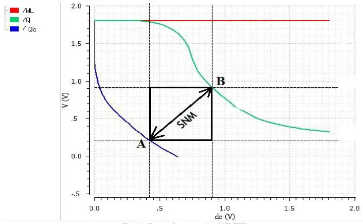
Fig.1. The standard setup for the SNM Calculation.
The SRAM to operate in read mode and write mode should have "readability" and "write stability" respectively. Above diagram shows the setup for SNM calculations. In which Both Inverters are biased with a variable voltage source that helps to analyse in different states, that is whether the cell stored logic ‘0’ or logic ‘1’. After this by making BL (Bit Line) and BLB (Bit Line Bar) at logic 0 or 1.i.e. low or high respectively.
The three different states work is as follows:
WRITE: The start of a write cycle begins by applying the value to be written to the bit lines. If we wish to write a 0, we would apply a 0 to the bit lines, i.e. setting BL bar to 1 and BL to 0. A 1 is written by inverting the values of the bit lines. WL is then asserted and the value that is to be stored is latched in. Note that the reason this works is that the bit line input-drivers are designed to be much stronger than the relatively weak transistors in the cell itself, so that they can easily override the previous state of the crosscoupled inverters.
Fig. 4. Butterfly curve for HOLD
HOLD(Standby): Fig .4.shows the SNM curve forHOLDor Standby statestate. If the word line is made low, the access transistors will disconnect the cell from the bit lines. The two cross coupled inverterswill continue to reinforce each other as long as they are connected to the supply.
ISSN(Online): 2320-9801
ISSN (Print) : 2320-9798
I
nternational
J
ournal of
I
nnovative
R
esearch in
C
omputer
and
C
ommunication
E
ngineering
(An ISO 3297: 2007 Certified Organization)
Vol. 4, Issue 7, July 2016
Read: Assume that the content of the memory is a 1, stored at Q. The read operation is done by using the sense
amplifiers that pull the data and produce the output. The row decoders and column decoders are used to select the appropriate cell or cells from which the data is to be read and are given to the sense amplifiers through transmission gate.
STATIC NOISE MARGIN OF SRAM
Noise margin can be defined using the input voltage to output voltage transfer characteristic (VTC). The static noise margin high and static noise margin low is defined as [7]
NMH = VOH - VIH …..(3.1) NML = VIL- VOL ….. (3.2)
where VIL is the maximum input voltage level recognized as logical ‘0’, VIH is the minimum input voltage level recognized as a logical ‘0’ VOL is the maximum logical ‘0’ output voltage, VOH is the minimum logical ‘1’
III.PROPOSED WORK
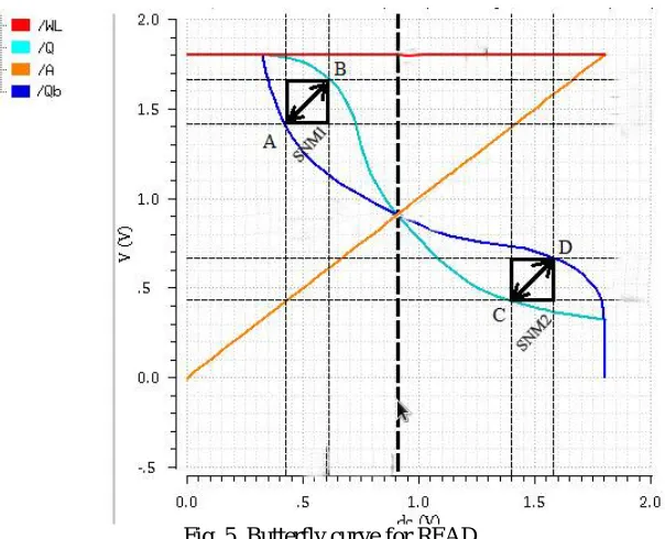
Fig.6, Shows the proposed 8T SRAM, in 6T SRAM. Two NMOS (M1 & M3) have been connected in series with already connected NMOS (M0 & M2) in latched inverter. Connecting Transistor in this way is to reduce leakage current as this will increase the resistance of current path, when the NMOS is in cut-off region. So reduce the leakage current and improve stability of SRAM cell. In this work we have scaled supply voltage and analyse the effect of supply voltage on Energy and Power consumption. In SNM curves in Fig4 and Fig 5, square box is fit and marked some points namely A,B,C,D on Q vsQb curves. In which A is less than B & C is less than D. Differences of this points gives the value of SNM1 & SNM2. We estimate the SNM by calculating the node voltage at read cycle (VOL) and the turnon voltage when the state transition begins (VOH) [12].
In this configuration Pass transistor M5 & M4 are adjusted such that they neither stronger than NMOS nor PMOS. Width of PMOS M7 & M6, kept higher than pass transistor and Nmos.
Then on different mode that is Read, Write & Hold mode,the butterfly curve made, and power and energy is calculated.
Fig.7. Comparison of Q &QB at different Vdd in Write Mode
Fig.8. Comparison of Q&Qb at different Vdd in READ Mode
IV.SIMULATION RESULTS
ISSN(Online): 2320-9801
ISSN (Print) : 2320-9798
I
nternational
J
ournal of
I
nnovative
R
esearch in
C
omputer
and
C
ommunication
E
ngineering
(An ISO 3297: 2007 Certified Organization)
Vol. 4, Issue 7, July 2016
1. READ MODE -
VDD Power (Conventional) Power(Present Work) Energy
(Conventional)
Energy (proposed)
1.8 195.0 E-06 126.7E-06 92.63E-06 53.86E-06
1.5 105.2 E-06 66.53E-06 38.43 E-06 21.68E-06
1.0 20.25 E-06 11.93E-06 3.860 E-06 2.04E-06
0.9 12.06 E-06 6.946E-06 1.913 E-09 994.7E-09
0.5 205.8 E-09 113.7 E-09 12.64 E-09 6.519E-09
2. WRITE MODE –
VDD Power (Conventional) Power (Present Work) Energy
(Conventional)
Energy (proposed)
1.8 175.4 E-06 141.2 E-06 156.7 E-06 137.3 E-06
1.5 99.39 E-06 72.94 E-06 82.40 E-06 58.82 E-06
1.0 16.53 E-06 12.37 E-06 7.411 E-06 6.501 E-06
0.9 9.567 E-06 07.02 E-06 3.725 E-06 3.266 E-06
0.5 125.9 E-09 74.84 E-09 16.79 E-09 13.66 E-09
3.HOLD MODE –
VDD Power (Conventional) Power (Prosed Work) Energy
(Conventional)
Energy (proposed)
1.8 175.4 E-06 18.53E-06 156.7 E-96 17.05E-06
1.5 9.974 E-06 6.104E-06 8.245 E-06 4.730E-06
1.0 360.2 E-09 206.5E-09 202.3 E-09 109.8E-09
0.9 130.8 E-09 75.43E-09 066.6 E-09 33.33E-12
0.5 895.7 E-012 556.6E-12 260.3 E-12 151.6E-12
V. CONCLUSION AND FUTURE WORK
As the conventional have number of drawbacks like more power consumption, increased leakage current, noise problem,8T SRAM with this technique called stackinghelps to reduce leakage current, power consumption is introduced. We have shown the power consumption comparison between our proposed Cell with convention logic at 180nm standard CMOS technology.This paper represent 53% static power reduction at 1.8v in read. 24.2% reduction in Write mode at 1.8v.
REFERENCES
1. R. W. Keyes, “The effect of randomness in the distribution of impurity atoms on FET threshold,” App. Phys., vol. 8, pp. 251–259, 1975.
2. T. Mizuno, J. Okamura, and A. Toriumi, “Experimental study of threshold voltage fluctuations using an 8K MOSFET array,” in Proc. Symp. VLSI Tech., Jun. 1993, pp. 41–42.
3. X. Tang, V. De, and J. D. Meindl, “Intrinsic MOSFET parameter fluctuations due to random dopant placement,” IEEE Trans. VLSI Syst., vol. 5, pp. 369–376, Dec. 1997J.
4. A. P. Chandrakasan el al., “Low-power CMOS digital design,” IEEE Journal of Solid-state Circuits”, Vol. 27, pp. 473-484, Apr. 1992.
5. J. Lohstroh, E. Seevinck, and J. Groot, “Worst-case noise margin criteria for logic circuits and their mathematical equivalence,” IEEE J. Solid State
Circuits, vol. SC-18, pp. 803–806, Dec. 1983A. Yang and L. Kim, “A low-power SRAM using hierarchical bit line
andlocalsenseamplifiers,”IEEEJ.Solid-StateCircuits,vol.40,no.6, pp. 1366–1376, Jun. 2005
6. Lee, D. Blaauw, and D. Sylvester, "Gate oxide leakage current analysis and reduction for VLSI circuits," IEEE Trans. on Very Large Scale Integration
7. J. Rabaey, A. Chandrakasan, and B. Nikolic, Digital Intergrated Circuits: A Design Perspective, 2nd ed. Englewood Cliffs, NJ: Prentice-Hall, 2003
8. E.Seevinck,“Static-noisemarginanalysisofMOSSRAMcells,”IEEE J. Solid-State Circuits, vol. SC-22, no. 5, pp. 748–754, Oct. 1987.
9. Andrei Pavlov &ManojSachdev, “CMOS SRAM Circuit Design and Parametric Test in Nano-Scaled Technologies”. Intel Corporation, University of
Waterloo, 2008 Springer Science and Business Media B.V., pp:1-202.
10. A. P. Chandrakasan el al., “Low-power CMOS digital design,” IEEE Journal of Solid-state Circuits”, Vol. 27, pp. 473-484, Apr. 1992
11. T. Sakurai, “High-speed circuit design with scaled-down MOSFET’s and low supply voltage,” in Proc. IEEE Int. Symp. Circuits Syst., May 1993, pp.