Electric-field-induced point defect redistribution in single-crystal TiO
2–xand
effects on electrical transport
Ali Moballegh
⇑and Elizabeth C. Dickey
Department of Materials Science and Engineering, North Carolina State University, Raleigh, NC 27606, USA
Received 13 August 2014; revised 28 October 2014; accepted 20 November 2014 Available online 14 January 2015
Abstract—The spatial redistribution of non-stoichiometric point defects in rutile TiO2is studied as a function of voltage and time. Single crystals are
equilibrated initially to a well-defined stoichiometry with n-type conductivity and a carrier concentration on the order of 1018cm3. The crystals are subsequently electroded with Pt contacts that exhibit Schottky behavior. When subjected to an applied voltage of 15 V, a time-dependent increase and saturation in the leakage current is observed, which is associated with an accumulation of point defects and an attendant decrease in stoichi-ometry at the cathode electrode. This local change in stoichistoichi-ometry degrades the Schottky barrier, leading to asymmetric electrodes and thus mac-roscopic rectifying behavior. Cathodoluminescence spectroscopy shows that Ti interstitials dominate the point defect redistribution process. Under larger applied voltages, of around 30 V, qualitatively different behavior is observed in which the resistivity increases as a function of time. This behav-ior is associated with condensation of point defects into a region of extended defects and Magne´li phases near the cathode, sufficient to increase the bulk stoichiometry and resistivity. These experiments demonstrate that a one-dimensional drift-diffusion process, as opposed to filamentary growth, dominates in these experimental conditions and that the Pt–TiO2–Pt system remains closed, with no significant oxygen transport across the Pt–TiO2
interfaces. We believe this is the first observation of a second higher-voltage regime in which the bulk stoichiometry and thus resistivity is increased as large concentrations of defects condense into metallic Magne´li phases in the near-electrode regions.
Ó2014 Acta Materialia Inc. Published by Elsevier Ltd. All rights reserved.
Keywords:Oxides; Electromigration; Point defects; Electrical properties; Analytical electron microscopy
1. Introduction
The performance of electroceramic devices is largely determined by the thermodynamic and transport behaviors of coupled point and electronic defects in the material. Under direct current (DC) voltage these charged defects can redistribute spatially as a function of time. This phe-nomenon has been studied in numerous dielectric materials, such as TiO2[1–3], BaTiO3[4,5]and SrTiO3[6,7]. Although lattice defect migration can lead to detrimental behavior such as leakage current enhancement in capacitor devices
[4], it can also be utilized to form novel functional behav-iors, such as resistive switching in metal oxides[8–10].
Typically, electrodes for dielectric materials are chosen such that they lead to interface Schottky barriers that limit charge carrier injection into the dielectric. Seminal work in the 1990s by Waser et al. showed that point defect migra-tion under applied bias in BaTiO3and SrTiO3leads to an accumulation of charged point defects at the dielectric-elec-trode interface, modifying the interface characteristics
[6,11]. The local accumulation of point defects near the interface can modify the Schottky barrier and width of
the depletion layers [12]which increases the electron injec-tion. The conduction mechanism itself can be modified in these highly defective regions[13]. Further, the asymmetri-cal behavior at the anode and cathode can lead to diode-like rectification behavior [1,2,4]. This functionality can be utilized for electronic devices, such as cross-bar array-type memory devices[14,15].
Several studies have quantitatively modeled the temporal ionic point defect redistribution under voltage biasing by solving the drift-diffusion equation in a time domain and considering ionic transport behavior across the interface as a boundary condition within the dilute solution approxima-tion[8,11,16–18]. If, however, the electrodes block or limit mass transport across the interface, then very high concen-trations of point defects may accumulate, well beyond a dilute concentration, and may even push the ion activity out-side of the material’s stability range. Several experimental studies have, in fact, shown condensation of point defects into higher-dimensional defects or ordered structures near electrodes as a consequence of DC biasing[3,19–22].
The present work focuses on point defect migration in TiO2, a material that has attracted intense interest in diverse applications such as capacitors, where its high dielectric constant is influenced from the unique arrange-ment of the TiO6-octahedra, and memristor/resistive switching memory, with the ability of unipolar [23] or
http://dx.doi.org/10.1016/j.actamat.2014.11.032
1359-6462/Ó2014 Acta Materialia Inc. Published by Elsevier Ltd. All rights reserved. ⇑Corresponding author. Fax: +1 919 515 7724; e-mail: amoball@
ncsu.edu
Available online at www.sciencedirect.com
ScienceDirect
Acta Materialia 86 (2015) 352–360
bipolar[8,15,24]switching. Regardless of the form of TiO2 (amorphous, polycrystalline, single crystal), the governing model for resistive memory behavior has been the electro-formation of conductive (substoichiometric) filaments that shunt the anode and cathode, leading to a low-resistance state. As the local stoichiometry near the electrodes is mod-ulated with subsequent applied fields, the rectification behavior of the Schottky contacts can be manipulated
[15]. Jameson et al.[1]demonstrated Schottky barrier mod-ulation at the electrodes via local reduction/oxidation of TiO2, with electrical measurements on TiO2single crystals with surface-patterned Pt electrodes. The field-programma-ble rectification behavior was observed after voltage biasing at fields of 125–375 kV cm1 at room temperature. The behavior was also demonstrated to be reversible by revers-ing the polarity of the programrevers-ing voltage. Szot et al.[10]
provided a critical review of resistive switching in TiO2 and emphasized the need for more fundamental research aimed at understanding the mechanisms of defect transport and phase stability in these materials, since prior work on TiO2spanned materials with various degrees of crystallin-ity, purcrystallin-ity, etc. They emphasized the significance of the small stoichiometry range for rutile TiO2–xand the
forma-tion of crystallographic shear planes and Magne´li phases to accommodate the substoichiometry resulting from electrochemical reduction at the cathode. The authors pre-sented further work on heavily reduced single-crystal TiO2, annealed under different conditions with concomitant differences in initial stoichiometry. It was demonstrated with surface Pt electrodes that conductive, substoichi-ometry filaments were formed as well as crystallo-graphic shear defects and Magne´li phases at the cathode interfaces.
While a substantial body of literature already exists on point defect dynamics in TiO2, there has been significant disconnect between this body of literature and the abun-dant information known about point defect energetics and mobilities in rutile TiO2 [25–28]. This work aims to help bridge that gap by providing new and more general-ized insight into the mechanisms of point defect electromi-gration in TiO2. Ultimately, we aim to provide experimental data and guidance for future studies, which could predict quantitatively the time-dependent evolution of point defect redistribution under an applied electric field. We specifically focus on point defect transport behavior in single-crystal rutile TiO2 with well-defined initial-state defect chemistries and electrode geometries that interrogate the bulk (as opposed to surface) defect transport kinetics.
In addition, while prior literature almost exclusively considers the role of oxygen vacancies in the transport pro-cess, we also consider the role of titanium interstitials, which are known to dominate the point-defect equilibria at low oxygen activities [25–28]. Further, in contrast to the many perovskites in which cation interstitials are rela-tively immobile[4,6,29–31], both oxygen vacancies and tita-nium interstitials have significant mobility in rutile TiO2–x [32,33]. Referring to transition-state theory calculations, the titanium interstitial has lower migration energies, 0.225 eV along <1 1 0> and 0.37 eV along <0 0 1>[34], com-pared to the oxygen vacancy, 0.69 eV along <1 1 0> and 1.77 eV along <0 0 1>. As shown experimentally by Lee and Yoo[35], two different relaxation times are observed for TiO2during equilibrium with the external oxygen par-tial pressure due to the diffusivity of oxygen vacancies being one order of magnitude lower than titanium interstitials.
In the present work, the local interface microstructure and microchemistry are studied as a function of the degra-dation process via electron microscopy, diffraction and spectroscopy to gain insight into point defect transport and its role in the contact and electrical transport evolu-tion. We make no a priori assumptions about mechanisms of defect redistribution (i.e. homogeneous or filamentary growth) and show that in these well-defined and largely homogeneous materials a 1-D homogeneous modulation of the interface chemistry dominates under the conditions studied and is sufficient to describe the degradation process. In this mode of degradation we observe two regimes: one in which the electrical transport is dominated by local changes near the electrodes and another in higher-voltage regimes where large concentrations of point defects condense near the electrodes. In these higher-voltage ranges, the bulk stoi-chiometry is altered to the extent that it begins to dominate the electrical transport.
2. Experimental procedure
High-purity (1 0 0)-oriented rutile TiO2 single crystals, made by the Verneuil growth process, were purchased from Shinkosha Company (Japan). The most significant impu-rity was reported to be Al at50 ppm by weight. The crys-tals, well polished with 1lm diamond paper, were annealed under specific oxygen partial pressure (pO2) and tempera-ture conditions to establish the initial defect chemistry state of the material, taking into account the known equilibra-tion kinetics in TiO2[25–28].
Specifically, a series of single-crystal rutile samples were annealed and equilibrated at apO2of 104atm at 1100°C for 36 h. In this temperature range and reducing atmo-sphere (1050–1350°C and pO2= 102–104atm), TiO2 is an n-type semiconductor with the ln(conductivity) vs.
pO2 having a 1/4 slope, consistent with fully charged oxygen vacancies as the dominant point defects, which are compensated by titanium vacancies [25–27]. The pO2 was controlled in a high-temperature tube furnace using an argon and argon/H2 forming gas and monitored by a commercial zirconia-based oxygen gas sensor. After equil-ibration, the samples were quenched to T< 300°C in the flowing reducing atmosphere to establish the initial defect chemistry state. The approximate quench rate was mea-sured to be 40°C s1 (1100–900°C), 7.5°C s1 (900– 700°C), 2°C s1 (700–400°C) and 0.5°C s1 (700– 250°C). While the oxygen vacancies and titanium intersti-tials are mobile in TiO2, the titanium vacancies are rela-tively immobile [26,27] and are not expected to participate in the subsequent lower-temperature, field-induced redistribution.
Pairs of electrodes were deposited on opposite lateral (0 1 0) surfaces (3 mm0.5 mm) by magnetron DC sput-tering to study transport along the [0 1 0] direction. A power density of 6.11 W cm2, a gas pressure of 30 mTorr (pure Ar) and a substrate to target distance of 3.4 cm were used in the deposition process, which resulted in a deposition rate of 75 nm min1for platinum. The deposited contacts, which covered the two lateral surfaces, were annealed at 200°C for 3 h to establish reproducible contacts at the TiO2–x/Pt interface [36]. Since the work function of Pt
The defect migration studies were performed at 200°C by applying a DC voltage using a HP-6634B power supply with 15–70 V, corresponding to average electric fields rang-ing from 100 to 500 V cm1. Throughout various points in the degradation process, the current–voltage (I–V) behav-ior was measured at room temperature over a voltage range of ±8 V by a high-precision Keithley 617 electrometer. The voltage was stepped in increments of 0.05 V and current measurements were made after 10 s to achieve steady state and avoid the effects of polarization currents.
The local microstructure and microchemistry in the near-electrode regions were studied by electron microscopy and spectroscopy. Cathodoluminescence (CL) spectroscopy was accomplished using a Gatan MonoCL4 with a highly sensitive photomultiplier tube (160–930 nm) detector on a Zeiss Evo 50 scanning electron microscope with a tungsten emitter. Site-selective transmission electron microscopy (TEM) samples were prepared by focused ion beam (FIB) from the TiO2–x/Pt interfaces before and after the
degrada-tion studies. Microstructural defects, formed after the deg-radation process, were studied using a JEOL transmission electron microscope equipped with a field emission gun (JEOL 2010F) operated at 200 kV. Electron energy loss spectroscopy (EELS) and scanning transmission electron microscopy (STEM) were performed in a monochromated FEI G2 Titan microscope operated at 200 kV. The EEL spectra were acquired in STEM mode with a collection angle of 39.1 mrad. The energy resolution of the EELS was measured to be about 0.2 eV, as determined with the full width at half maximum of the zero-loss peak. Energy dispersion of 0.1 eV per channel was used to record both Ti-L2,3 and O-K edges simultaneously. The Ti:O ratio was quantified by integrating the respective edges, after appropriate background subtraction for both Ti-L2,3 and O-K edges and using Hartree–Slater inelastic scattering cross-sections.
3. Results
3.1. Initial defect chemistry state and electrode boundary conditions
Fig. 1 shows a defect equilibrium diagram of TiO2, calculated from published equilibrium constants [25,28], considering the Al impurity level ([Al]1= 1.47106 per site) and the charge neutrality condition. The dia-gram includes the concentration of charged point defects and electronic carriers over a wide range of oxygen activ-ities (1020–102pO2). In the reduced region, three regimes are identified as a function of oxygen partial pressure: (i) the reduced regime, which is dominated by oxygen vacancies and titanium vacancies compensation ðV 2þ
O ¼2½V 4
Ti Þ, but where the electron carrier concentra-tion is governed by Ti interstitials; (ii) the strongly reduced regime, in which doubly ionized oxygen vacan-cies dominate, with an associated electron carrier concen-tration exponent equal to1/6 ð2½V 2þ
O ¼nÞ; and (iii) the extremely reduced regime, in which trivalent titanium interstitials are the dominant point defects, with the
pO2-dependent electronic carrier concentration exponent equal to 1/4 ð3½Ti3þ
i ¼nÞ.
The defect equilibria expected for annealing conditions of 104pO2and 1100°C are denoted by the vertical dashed line and correspond to: ½V 2þ
O ¼4:5810
3
ðper siteÞ,
½V 4
Ti ¼2:2910
3ðper siteÞ, ½Ti3þ
i ¼6:3610
7ðper siteÞ,
½Ti4þ
i ¼1:3710
5ðper siteÞ, n= 3.73105 (per site) or 1.791018cm3 andp= 4.46107(per site). Based on the electron carrier concentration, the bulk electrical resis-tivity,qB, is calculated to be 52X.cm, considering an
elec-tron mobility (le) of 6:7102cm2=V:s[28].
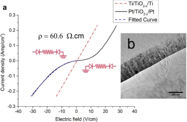
To corroborate the expected defect chemistry state, the bulk resistivities of equilibrated crystals were measured using Ti electrodes, which form ohmic contacts with TiO2. Fig. 2a (dashed red line) presents the resulting I–V characteristics measured at room temperature. The bulk resistivity is measured to be 60.6O.cm, which is within 16.5% of the expected value based onFig. 1.
For the remainder of the studies, approximately 300 nm thick symmetrical Pt contacts were used, as shown in the bright-field TEM image in Fig. 2b. The I–V curve of Pt/ TiO2–x/Pt (solid curve inFig. 2a) shows an initial
exponen-tial behavior, indicative of reverse-biased Schottky barriers at the TiO2–x/Pt interfaces.
TheI–Vbehavior of the Pt/TiO2–x/Pt cell was modeled
by an equivalent circuit consisting of two Schottky barriers in series with the bulk (ohmic) resistance, assuming therm-ionic emission over the interface barriers [12]. One of the Schottky interfaces is forward biased (Eq. (1)), while the other is reverse biased (Eq.(2)) and modeled by the Scho-ttky equation, taking into account the effects of image charge lowering (Eq.(3)):
JF ¼AT2exp qøBn
kT
exp qVF nkT
1
ð1Þ
JR¼AT2exp
q øBn ffiffiffiffiffiffi qEm 4ps q kT 2 6 4 3 7 5 ð2Þ Em¼ ffiffiffiffiffiffiffiffiffiffiffiffiffiffiffiffiffiffiffiffiffiffiffiffiffiffiffiffiffiffiffiffiffiffiffiffiffiffiffiffiffiffiffiffiffiffiffiffi 2qND s
VRubi kT
q
s
ð3Þ
øBn,A**,n,es,ubi,EmandNDare the barrier height,
effec-tive Richardson constant, ideality factor, dielectric permit-tivity, built-in potential, maximum electric field at the interface and carrier concentration at the interface,
respec-Fig. 1.Defect diagram for single-crystal TiO2 at 1100°C, where the
tively. The model was fitted to the experimentalI–Vdata by setting the parameters to independently measured or litera-ture values (i.e. measured bulk resistivity = 60.6O.cm,
A**= 1.2106(A m2K2)[41],e
s= 7.5[42]andn= 1).
The fitted values for the barrier height, built-in potential and carrier concentration at the reversed-biased electrode were 0.78 eV, 0.5 eV and 1.131019cm3, respectively. The dashed blue line inFig. 2a is the fitted curve with an
R2 value of 0.9984, and is almost indistinguishable from the experimental curve (solid black line).
In the lower voltage range, the reverse-biased electrode limits the conduction through the TiO2, and the fitted value of the Schottky barrier height is reasonable within the reported ranges for the electron affinity of TiO2 and the work function of Pt. The total resistivity converges to the bulk resistivity around 20 V cm1, as evidenced by the converging slope of theI–Vcurve (solid curve inFig. 2a) to the bulk linear resistivity (dashed red line in Fig. 2a). It should be noted that since both the bulk and reversed-biased electrodes significantly affect the I–V response, it was necessary to fit the experimental data to an equivalent circuit model with these two elements to extract the interface characteristics. The contributions of the forward bias electrode are insignificant for these samples.
3.2. Low electric-field degradation regime
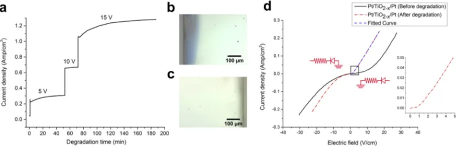
The Pt/TiO2–x/Pt sample was then subjected to DC field
degradation studies at 200°C. Fig. 3a shows the leakage current gradually increasing during the degradation process at 15 V bias voltage (75 V cm1) until it reaches a satura-tion of 1.3 A cm2 after several hours. An optical image of the negative terminal (Fig. 3b) shows that the TiO2–x
near the cathode interface becomes a dark blue color over a length scale of approximately 120lm, indicative of an increased concentration of Ti3+in that region[43]. In con-trast,Fig. 3c shows an optical image of the TiO2–x/anode
interface, where the TiO2–xremains colorless and
transpar-ent. TheI–V response of the degraded sample inFig. 3d displays a diode-like rectification behavior, with nearly
ohmic behavior in the positive bias direction when the cath-ode serves as the reverse-biased Schottky barrier. The bulk resistivity remains constant at 60.6O.cm.
Although the sample in the degraded state had an inho-mogeneous distribution of point defects, we still attempted to model theI–Vdata inFig. 3d to the three-element equiv-alent circuit model. The model was fitted to the positive part of theI–Vcurve, with the barrier height for the unde-graded sample, 0.78 eV, being used as the forward-biased electrode (anode during degradation). The parameters for the reverse-bias electrode (cathode during degradation) were refined, resulting in a fitted barrier height of 0.75 eV, a carrier concentration of 9.411019cm3, a built-in potential of 0.1 eV and an R2 fit value of 0.9999. The most significant difference in the contact characteristics from the undegraded samples is found in the built-in poten-tial term, which may be associated with the accumulation of positively charged point defects (titanium interstitials and oxygen vacancies) in that region, compensated by elec-trons that raise the local Fermi level. It should be men-tioned that this interpretation is considered only speculative at this point, as the interface barrier affects only a small portion of the totalI–Vbehavior and the fit to the linear part of the curve dominates theR2.
In principal, we should be able to use the fitted values from the positive part of the I–V curve and reverse the polarity on the equivalent circuit model to predict the I– Vresponse on the negative part of the curve. This approach does not, however, adequately reproduce the current response, achieving an R2value of only 0.6887. While the nearly ohmic contact, now in the forward-biased polarity, accounts for some of the increased current density in this polarity, it does not account for all of it.
To investigate changes in the local microchemistry, site-selective TEM samples were made via FIB lift-out from the TiO2–x/cathode interface region after the first-step-forward
degradation process. The Ti valence state and oxygen stoi-chiometry as a function of position from the cathode were measured using monochromated EELS mapping. Fig. 4a shows a set of EEL spectra acquired from the interface to 200 nm from the interface. The onset of the O K edge
Fig. 2. (a) The conductivity of TiO2single crystal, annealed at 1100°C for 36 h and 104pO2, with ohmic contacts (Ti/TiO2–x/Ti), is compared to the
Pt-deposited electrodes (Pt/TiO2–x/Pt), with Schottky barriers formed at the interfaces. (b) TEM image of single-crystal TiO2 after Pt contact
(532 eV) was used to calibrate the energy position of the spectra. Fig. 4b presents the quantified stoichiometry of TiO2–xas a function of position from the interface toward
the bulk. The stoichiometry reaches as low as TiO1.67, which is far outside the stability region of rutile and should correspond to a Magne´li phase of Ti3O5 [44,45]. Ordered phases in these regions have not been detected by TEM or electron diffraction, which may indicate a nucleation barrier to the Magne´li phase formation, although some extended defects such as dislocations are observed.
Also apparent in the EEL spectra ofFig. 4a is a signif-icant change in the energy onset and fine structure of the Ti-L2,3 edges near the interface, as compared to 200 nm from the interface. As shown inFig. 4b, a 0.7 eV chemical shift of Ti-L2,3edge toward lower energy is observed near the interface. This is consistent with a lowering of the Ti oxidation state, concomitant with the change in local stoi-chiometry[46,47].
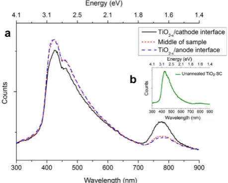
While EELS is useful for measuring local stoichiometry, it does not provide information regarding the type of point defects that are responsible for the substoichiometry, nor is it sensitive to subtle changes in stoichiometry that can lead to quite large changes in carrier concentrations. CL spec-troscopy is a complementary technique that is used to investigate energy levels related to the point defects and has been used to study defect states in n-type TiO2single
crystals[48]. The rutile TiO2CL spectrum exhibits a broad peak around 410 nm wavelength, 3 eV, which corre-sponds to the TiO2band gap[49]. The energy level of tita-nium interstitials ðTi3þ
i Þ is reported to be about 1.53 eV above the valence band and has an associated emission peak in the infrared region. The energy position of fully ionized oxygen vacancies is around 2.23–2.83 eV above the valence band where the associated emission peak lies within the tail of the band-gap emission[48,50].
Fig. 5presents the CL spectra taken from various regions in the TiO2–xcrystal after the first-step forward-degradation
process: adjacent to the cathode (solid black line), from the center of the sample (red dotted line) and adjacent to the anode (blue dashed line). The inset shows a CL spectrum from an as-received rutile single crystal, in which the peak intensity at 1.6 eV corresponds to Ti interstitials and is small relative to the intensity in the annealed sample (dashed red line in main figure). The spectra from the anode and sample center after degradation are almost identical, while a significant increase in the peak intensity at 1.6 eV is observed in the cathode region. Note the spatial resolution of the CL spectra is1lm, based on the interaction volume of the electron beam with the sample – much larger that the region probed by the EELS measurements. The CL spectra thus probe the broader darkened regions evident inFig. 3b. These data suggest thatðTi3þ
i Þdominates the defect
chemis-Fig. 4. (a) EEL spectra of single-crystal TiO2after 15 V degradation from a region adjacent to the cathode. (b) The oxygen content and chemical shift
of the Ti L2,3edge after degradation as a function of distance from the interface.
Fig. 3. (a) Conductivity of TiO2–xas a function of time for 5, 10 and 15 V biasing. (b) An optical image of the Pt–TiO2–xcathode region after 15 V
degradation. (c) An optical image of the Pt–TiO2–x anode region after 15 V degradation. (d)I–Vmeasurement before and after 15 V forward
try in the near-cathode region, even though oxygen vacancies were the dominant defect in the as-equilibrated state. This finding is consistent with the facts that Ti interstitials are more mobile than oxygen vacancies in the rutile lattice[35]
and that Ti interstitials become the preferred substoichio-metric defects at low oxygen activities (Fig. 1).
To assess the reversibility of the defect migration in the low electric field regime, another crystal was prepared iden-tically and studied in a forward and subsequent reverse deg-radation cycle. The forward-biased I–V characteristics (Fig. 6) are very similar in comparison to the data presented inFig. 3. When subjected to reverse biasing (dashed line in blue), the electrode behavior is nearly inverted, with the ori-ginal cathode (as defined during forward degradation) approaching, but not fully converging to, its original I–V
behavior (in black), suggesting that the stoichiometry changes in the near-cathode region are nearly reversible.
3.3. Moderate electric-field regime
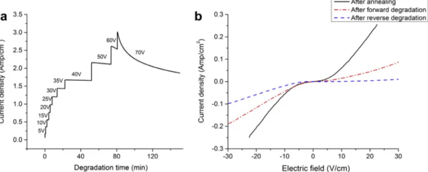
At higher levels of applied bias, qualitatively different behavior is observed and will therefore be discussed sepa-rately. A different set of thermally equilibrated samples were biased at higher voltage levels, 35–60 V (175– 300 V cm1electric field). After similar increases in leakage current at low fields, the samples then exhibit a decrease in the leakage current as a function of time at higher fields (Fig. 7a). Fig. 7b compares the I–V curves of the as-annealed sample after the second step (60 V) forward deg-radation. At high electric fields, where the total resistance is dominated by contributions from the bulk resistivity, we find the field-degraded sample to be much more resis-tive, which is unexpected. Fitting theI–Vcurve on the posi-tive voltage side yields a barrier height of 0.74 eV with negligible built-in potential, bulk resistivity of 203.01O.cm and anR2value of 0.9997.
To understand the origins of this qualitatively different behavior, we analyzed the microstructure and microchemis-try of the TiO2–x/cathode region. The TEM image in Fig. 8a shows that microstructural defects are formed near the interface, as a result of clustered point defects.Fig. 8b shows an electron diffraction pattern from the area, which exhibits superlattice reflections associated with 3d011 peri-odicity. This stacking sequence is seen in the STEM image (Fig. 8c) and is associated with point defect ordering into ordered crystallographic shear planes or Magne´li phases
Fig. 7. (a) Conductivity of TiO2–xas a function of time up to 60 V biasing. (b)I–Vcharacteristics before degradation but after 60 V forward biasing. Fig. 6. I–V characteristics before degradation, after 15 V forward
biasing and after 15 V reverse biasing.
Fig. 5.(a) Cathodoluminescence spectra of a degraded single-crystal TiO2 sample. The black curve is taken near the TiO2–x/cathode
interface; the red and blue curves are from the bulk and TiO2–x/anode
interface regions, respectively. (b) CL spectrum of as-received rutile TiO2single crystal. (For interpretation of the references to colour in
[45,51,52]. A model of the Ti3O5Magne´li phase associated with the 3d011sequence is inset inFig. 8d. Magne´li phase formation in severely degraded TiO2has been reported by Kwon et al. [51] and investigated by using the HRTEM and electron diffraction. The Magne´li phases are formed in extremely reduced TiO2–x, thereby accommodating the
large concentrations of point defects. Important to this study is the fact that the Magne´li phases exhibit a
metal–insulator transition and most are metallic at room temperature, including Ti3O5[44,51].
We can rationalize the decrease in the leakage current (Fig. 7a) in terms of the point defect condensation into Magne´li phases near the cathode, which leaves the bulk crystal with lower defect concentrations and thus higher bulk resistivity. The voltage drop across the metallic Mag-ne´li phase is negligible and in effect serves to extend the contact. As the bulk resistivity increases – an almost three-fold increase is measured experimentally – the bulk starts to dominate theI–Vbehavior.
Fig. 9shows a schematic illustration of defect redistribu-tion over the degradaredistribu-tion process. Using a simple mass-bal-ance calculation, the following analysis helps validate our hypothesis that the bulk defect concentrations are lowered by the defect condensation process near the cathode. First, the electron concentration and substoichiometry in the bulk necessary to explain the 203.01O.cm bulk resistivity are
n= 1.11018(cm3) and TiO
1.9998, respectively. We then consider the oxygen vacancy concentration needed to form Ti3O5to be 5.81021cm3, whereas the initial concentra-tion of the oxygen vacancies before the degradaconcentra-tion process was 7.81017cm3. Assuming no significant oxygen trans-fer at the electrodes or solid/gas interface, a simple mass balance would predict a thickness of the highly conductive Magne´li phase to be about 200 nm at the cathode interface, which is in excellent agreement with the thickness of the extended defect phase inFig. 8a. Not only does this explain the origins of the observed increase in leakage current in the
Fig. 8. (a) TEM image revealing microstructural defects induced from clustering of positively charged point defects near the cathode. (b) Diffraction patterns showing long-range ordering of point defects near the cathode with a periodicity of 3d011. (c) STEM images showing corresponding
crystallographic shear planes corresponding to Magne´li phases (d) at the electrode.
Fig. 9. A schematic of defect redistribution over the high-field degradation process. The red dotted line corresponds to the initial defect concentration and the blue solid line to the spatial distribution after 60 V biasing. The accumulation of defects near the cathode region depletes the bulk concentration of defects. (For interpretation of the references to colour in this figure legend, the reader is referred to the web version of this article.)
Fig. 10. (a) Conductivity of TiO2–x as a function of time up to 70 V after reversing the polarity with respect to that shown inFig. 7. (b)I–V
moderate field degradation regime, but it also points to the fact that the dense Pt electrodes are impermeable to oxygen transfer across the interface.
The final experiment tested the reversibility of the defect migration in this moderate-field regimen by applying an equivalent bias (350 V cm1) to the sample but in the reverse polarity. Fig. 10a shows the leakage current as a function of time, monitored over the reverse-bias degrada-tion at 200°C. As observed in the forward-bias degrada-tion, the leakage current significantly decreases at 70 V.
Fig. 10b compares the corresponding I–V curves of the sample before degradation, after the second-step-forward bias and after reverse bias, where we see that the bulk resis-tivity continues to increase. After reverse degradation, TEM analysis of both electrodes (not shown) revealed extended defects at both electrodes. Thus, under the condi-tions studied, the extended defects at the original cathode are metastable and do not convert back to rutile TiO2–x,
while extended defects form at the opposite electrode, anal-ogous to their formation in the forward-bias experiment. The result of this defect condensation process is that the bulk defect concentration continues to drop, driving up the bulk resistivity.
4. Conclusions
At low electric-field degradation, there is clear evidence for the accumulation of substoichiometric point defects at the cathode electrode in single-crystal TiO2. The defect redistribution is largely homogeneous (a 1-D drift-diffusion mechanism), with no evidence for substoichiometric filament formation. While oxygen vacancies are widely implicated as the important point defect in the kinetics of this process, this work points to the significance of titanium interstitials, even when they are a minority defect in the vir-gin sample. Titanium interstitials dominate the redistribu-tion process for both thermodynamic and kinetic reasons: they are energetically favorable at low oxygen activities as encountered in the near-cathode region and have higher diffusivity [34,35]. Even at relatively low applied voltages (15 kV), the stoichiometry within 100 nm of the cathode region is well below the stability of TiO2, as measured by EELS. This is indicative of Magne´li phase formation; how-ever, there appears to be a nucleation barrier to their for-mation, which was not overcome in low-field studies. The accumulation of defects near the cathode results in signifi-cantly altered Schottky barrier characteristics via the built-in potential and macroscopic rectification behavior.
At higher applied voltages (50 V) we observe qualita-tively different temporal behavior of the leakage current. In this regime, the high-field current is found to decrease with time. As a result of the severe degradation, microstruc-tural defects are induced by the condensation of large con-centrations of point defects to the extent that the bulk stoichiometry is significantly altered, making it more stoi-chiometric and thus more resistive. Interpretation of the
I–Vbehavior via simple mass-balance calculations explains the observed behavior and shows dense Pt electrodes block ion transfer, leading to a closed system.
Finally, reverse degradation shows that the Magne´li phase formation near the cathode is not reversible at 200°C for the times and fields studied, indicative of a nucleation barrier associated with the phase transition.
Acknowledgements
This work was supported by the National Science Foundation under grant number DMR-1132058. We acknowledge the NCSU Analytical Instrumentation Facility. Special thanks and gratitude goes to Thomas Podbesek, who assisted in contact deposition.
References
[1]J.R. Jameson, Y. Fukuzumi, Z. Wang, P. Griffin, K. Tsunoda, G.I. Meijer, Y. Nishi, Appl. Phys. Lett. 91 (2007) 112101.
[2]J.J. Yang, M.D. Pickett, X.M. Li, D.A.A. Ohlberg, D.R. Stewart, R.S. Williams, Nat. Nanotechnol. 3 (2008) 429. [3]K. Szot, M. Rogala, W. Speier, Z. Klusek, A. Besmehn, R.
Waser, Nanotechnology 22 (2011) 254001.
[4]G.Y. Yang, G.D. Lian, E.C. Dickey, C.A. Randall, D.E. Barber, P. Pinceloup, M.A. Henderson, R.A. Hill, J.J. Beeson, D.J. Skamser, J. Appl. Phys. 96 (2004) 7500. [5]J. Ro¨del, G. Tomandl, J. Mater. Sci. 19 (1984) 3515. [6]R. Waser, T. Baiatu, K.H. Hardtl, J. Am. Ceram. Soc. 73
(1990) 1654.
[7]W. Jiang, M. Noman, Y.M. Lu, J.A. Bain, P.A. Salvador, M. Skowronski, J. Appl. Phys. 110 (2011) 034509.
[8]D.S. Jeong, H. Schroeder, R. Waser, Phys. Rev. B 79 (2009) 195317.
[9]T. Menke, P. Meuffels, R. Dittmann, K. Szot, R. Waser, J. Appl. Phys. 105 (2009) 066104.
[10]R. Waser, R. Dittmann, G. Staikov, K. Szot, Adv. Mater. 21 (2009) 2632.
[11]T. Baiatu, R. Waser, K.-H. Ha¨rdtl, J. Am. Ceram. Soc. 73 (1990) 1663.
[12]S.M. Sze, K.K. Ng, Physics of Semiconductor Devices, Wiley-Interscience, Hoboken, NJ, 2007.
[13]W. Liu, G.-Y. Yang, C.A. Randall, Jpn. J. Appl. Phys. 48 (2009) 051404.
[14]G.H. Kim, K.M. Kim, J.Y. Seok, M.H. Lee, S.J. Song, C.S. Hwang, J. Electrochem. Soc. 157 (2010) G211.
[15]J.J. Yang, J. Borghetti, D. Murphy, D.R. Stewart, R.S. Williams, Adv. Mater. 21 (2009) 3754.
[16]D. Strukov, R.S. Williams, Appl. Phys. A 94 (2009) 515. [17]R. Meyer, R. Liedtke, R. Waser, Appl. Phys. Lett. 86 (2005)
112904.
[18]L. Zhang, Z.J. Chen, J.J. Yang, B. Wysocki, N. McDonald, Y.R. Chen, Appl. Phys. Lett. 102 (2013) 153503.
[19]C.L. Jia, M. Lentzen, K. Urban, Science 299 (2003) 870. [20]O.T. Sørensen, Nonstoichiometric Oxides, Academic Press,
New York, 1981.
[21]Z. Zhang, W. Sigle, M. Ru¨hle, Phys. Rev. B 66 (2002) 094108.
[22]D.I. Woodward, I.M. Reaney, G.Y. Yang, E.C. Dickey, C.A. Randall, Appl. Phys. Lett. 84 (2004) 4650.
[23]H. Schroeder, D.S. Jeong, Microelectron. Eng. 84 (2007) 1982.
[24]Y.H. Do, J.S. Kwak, Y.C. Bae, K. Jung, H. Im, J.P. Hong, Appl. Phys. Lett. 95 (2009) 093507.
[25]T. Bak, J. Nowotny, M.K. Nowotny, J. Phys. Chem. B 110 (2006) 21560.
[26]M.K. Nowotny, T. Bak, J. Nowotny, J. Phys. Chem. B 110 (2006) 16270.
[27]M.K. Nowotny, T. Bak, J. Nowotny, J. Phys. Chem. B 110 (2006) 16292.
[28]M.K. Nowotny, L.R. Sheppard, T. Bak, J. Nowotny, J. Phys. Chem. C 112 (2008) 5275.
[29]A.V. Polotai, T.H. Jeong, G.Y. Yang, E.C. Dickey, C.A. Randall, P. Pinceloup, A.S. Gurav, J. Electroceram. 23 (2009) 6.
[31]G.I. Meijer, U. Staub, M. Janousch, S.L. Johnson, B. Delley, T. Neisius, Phys. Rev. B 72 (2005) 155102.
[32]E. Cho, S. Han, H.-S. Ahn, K.-R. Lee, S.K. Kim, C.S. Hwang, Phys. Rev. B 73 (2006) 193202.
[33]P. Kofstad, J. Phys. Chem. Solids 23 (1962) 1579.
[34]H. Iddir, S. O¨ g˘u¨t, P. Zapol, N.D. Browning, Phys. Rev. B 75 (2007) 073203.
[35]D.K. Lee, H.I. Yoo, Solid State Ionics 177 (2006) 1. [36]H. Muta, J. Jpn, Appl. Phys. 17 (1978) 1089. [37]L.R. Velho, R.W. Bartlett, Metall. Trans. 3 (1972) 65. [38]W.G. Kim, S.W. Rhee, Microelectron. Eng. 87 (2010)
98.
[39]J.G. Mavroides, D.I. Tchernev, J.A. Kafalas, D.F. Kolesar, Mater. Res. Bull. 10 (1975) 1023.
[40]D.O. Scanlon, C.W. Dunnill, J. Buckeridge, S.A. Shevlin, A.J. Logsdail, S.M. Woodley, C.R.A. Catlow, M.J. Powell, R.G. Palgrave, I.P. Parkin, G.W. Watson, T.W. Keal, P. Sher-wood, A. Walsh, A.A. Sokol, Nat. Mater. 12 (2013) 798. [41]J.A. Becker, Rev. Mod. Phys. 7 (1935) 95.
[42]C. Lee, X. Gonze, Phys. Rev. B 49 (1994) 14730.
[43]V.M. Khomenko, K. Langer, H. Rager, A. Fett, Phys. Chem. Miner. 25 (1998) 338.
[44]F.C. Walsh, R.G.A. Wills, Electrochim. Acta 55 (2010) 6342. [45]L.A. Bursill, B.G. Hyde, Prog. Solid State Chem. 7 (1972)
177.
[46]R.D. Leapman, L.A. Grunes, P.L. Fejes, Phys. Rev. B 26 (1982) 614.
[47]R.D. Leapman, L.A. Grunes, Phys. Rev. Lett. 45 (1980) 397. [48]I. Ferna´ndez, A. Cremades, J. Piqueras, Semicond. Sci.
Technol. 20 (2005) 239.
[49]J.K. Burdett, T. Hughbanks, G.J. Miller, J.W. Richardson, J.V. Smith, J. Am. Chem. Soc. 109 (1987) 3639.
[50]R. Plugaru, A. Cremades, J. Piqueras, J. Phys. Condens. Mat. 16 (2004) S261.
[51]D.H. Kwon, K.M. Kim, J.H. Jang, J.M. Jeon, M.H. Lee, G.H. Kim, X.S. Li, G.S. Park, B. Lee, S. Han, M. Kim, C.S. Hwang, Nat. Nanotechnol. 5 (2010) 148.