ABSTRACT
YANG, XIANGYU. Dielectrics and Interface Engineering for Silicon Carbide Metal Oxide Semiconductor Field Effect Transistors. (Under the direction of Dr. Veena Misra.)
Silicon carbide (SiC) is one of the most promising substrate materials for future power
switching devices due to its wide bandgap, high thermal conductivity and high breakdown
electrical field. SiC metal oxide semiconductor field effect transistor (MOSFET) has been
researched for decades. However, the achieved electron mobility on the silicon face of
4H-SiC remains low. Typical 4H-SiC MOSFETs use thermally grown oxide (SiO2) as the gate oxide.
High density interface states (Dit) near the conduction band edge leads to poor SiC MOSFET
mobility and the origin of the Dit is attributed to various carbon related defects formed during
high temperature oxidation. In this work, to avoid defects associated with thermal oxidation,
low temperature SiO2 deposited by atomic layer deposition (ALD) has been investigated as
the gate dielectric for SiC MOS devices.
The impacts of nitrogen and nitrous oxide (N2O) post deposition anneal (PDA) on the ALD
SiO2 properties were studied. It has been found that the ALD SiO2 shows negative effective
charges on n-type SiC resulting in high flatband voltage. High temperature N2O PDA
improves the overall dielectric properties and reduces the negative effective charge density.
With ALD SiO2 after N2O PDA, similar field effect mobility has been achieved with higher
threshold voltage as compared to the conventional SiC transistors with thermal oxide after
nitric oxide (NO) anneal.
Various interface engineering techniques have been developed to achieve high threshold
achieved. A novel interface engineering process using lanthanum silicate (LaSiOx) has been
demonstrated and reported for the first time. The incorporation of an ultra thin LaSiOx layer
dramatically improves the field effective mobility. More than 130 cm2/V*s peak mobility
with a VT of 3.1 V has been achieved using this LaSiOx interface engineering. The electron
mobility of MOSFET with optimized LaSiOx/ALD SiO2 dielectric stack is limited by the
phonon scattering, whereas mobility with only ALD SiO2 is limited by the coulomb
scattering.
The ALD SiO2/Al2O3 electrical dipole effect was explored for SiC MOSFET threshold
voltage tuning. The ALD SiO2/Al2O3 dipole was demonstrated on SiC for the first time. The
by Xiangyu Yang
A dissertation submitted to the Graduate Faculty of North Carolina State University
in partial fulfillment of the requirements for the degree of
Doctor of Philosophy
Electrical Engineering
Raleigh, North Carolina
2015
APPROVED BY:
_______________________________ ______________________________
Dr. Veena Misra Dr. Alex Huang
Committee Chair
________________________________ ________________________________
DEDICATION
To my parents
BIOGRAPHY
Xiangyu Yang was born in Taian, Shandong, China. He received the Bachelor’s degree in
Electrical Engineering from Shandong University, Jinan, China. He enrolled in the graduate
program in Electrical Engineering at North Carolina State University. His research focuses
on ALD dielectrics and interface engineering for SiC metal oxide semiconductor field effect
ACKNOWLEDGEMENTS
I would like to thank all individuals who have provided me with help and support throughout
my career. First and foremost, I wish to express my gratitude to my adviser Dr. Veena Misra
for her guidance and support I have received in completing my research. I am grateful to Dr.
Dickey, Dr. Huang and Dr. Muth for serving on my committee.
I would like to express my appreciation to my current and past group members, especially Dr.
Bongmook Lee, Dr. Srikant Jayanti, Dr. Daniel Lichtenwalner, Narayanan Ramanan, Steven
Mills and Dr. Smita Sarkar. I am thankful to my friends Dr. Gerd Duscher, Dr. Sid Mal, Dr.
Thomas Rawdanowicz, Dr. Tsung-Han Yang, Xinning Wang, Dr. Chi-Kai Chiu and Jeff Zhu
for their help and encouragement. I would like to acknowledge Toyota Motor Corporation for
funding my research and Cree Inc. for their high quality SiC substrates.
TABLE OF CONTENTS
LIST OF TABLES ... vii
LIST OF FIGURES ... viii
Chapter 1 Review of 4H-SiC MOSFETs ... 1
1.1 Overview of SiC and devices ... 1
1.2 Mechanisms of Mobility Degradation ... 9
1.3 Mobility Enhancement: Nitridation ... 13
1.4 Mobility Enhancement: Phosphorus Treatment ... 16
1.5 Mobility Enhancement: Group1 Metal Ions Incorporation ... 17
1.6 Mobility Enhancement: Deposited Dielectrics ... 18
1.7 Progress of 4H-SiC MOSFETs on other faces ... 20
1.8 Research goals and tasks ... 21
1.9 Summary of the Introduction ... 22
1.10 References ... 23
Chapter 2 Experimental Procedures and Methodology ... 28
2.1 Device structures ... 28
2.2 Dielectric deposition ... 32
2.3 Gate electrode deposition ... 35
2.4 MOS capacitor C-V characterization ... 36
2.5 MOS capacitor I-V characterization ... 39
2.6 MOSFET characterizations ... 40
2.7 Interface states density measurement ... 42
2.8 Analytical characterizations of dielectrics ... 44
2.9 Summary ... 47
2.10 References ... 47
Chapter 3 Properties of Low Temperature SiO2 Deposited by ALD for SiC MOS Devices . 49 3.1 Study of ALD SiO2 on Si ... 51
3.2 Optimization of ALD SiO2 on Si using N2O RTA ... 57
3.3 Initial study of electrical properties of ALD SiO2 on n-type SiC ... 60
3.4 N2O anneal of SiO2 on SiC ... 68
3.5 Electrical properties of ALD Al2O3 on SiC ... 78
3.6 References ... 84
Chapter 4 Novel Dual-Layer Dielectrics for Threshold Voltage Tuning of SiC MOS Devices ... 86
4.2 Concept of the cancelation and neutralization effect ... 91
4.3 Dual-layer capacitor results on SiC ... 95
4.4 References ... 101
Chapter 5 Electrical Properties of SiC Lateral MOSFETs Using ALD SiO2 as the Gate Dielectric ... 103
5.1 Lateral MOSFETs fabrication processes ... 103
5.2 MOSFETs using ALD SiO2 as the gate dielectric ... 105
5.3 MOSFETs using ALD SiO2/ Al2O3 stack as the gate dielectric ... 110
5.4 References ... 113
Chapter 6 Study of Lateral MOSFET Using SiO2 Related Interface Engineering for Electron Mobility Enhancement ... 114
6.1 Interface engineering using rapid thermal oxidation ... 114
6.2 Interface engineering using doped SiO2 by RF sputtering ... 122
6.3 References ... 132
Chapter 7 Study of Lateral MOSFET Using Lanthanum Silicate Interface Engineering for Mobility Enhancement ... 134
7.1 Properties of lanthanum silicate on SiC ... 134
7.2 Electrical characteristics of SiC MOSFETs with LaSiOx ... 144
7.3 References ... 156
Chapter 8 Investigation of Carrier Transportation and Threshold Voltage Reliability of Lateral MOSFETs Using ALD SiO2 as the Gate Dielectric and Various Interface Engineering Techniques ... 157
8.1 Dominant carrier scattering process ... 157
8.2 VT instability study ... 163
8.3 References ... 173
Chapter 9 Conclusions and Future Work ... 174
9.1 Conclusions ... 174
LIST OF TABLES
Table 1.1. Material properties common SiC polytypes. ... 1
Table 1.2. Material properties Si, 4H-Si and Wurztite GaN. ... 3
Table 1.3. Temperature dependence of four mobility components. ... 11
Table 3.1. Extracted ALD SiO2 bandgap and band alignment parameters. ... 68
Table 3.2. Effective charge density of ALD SiO2 on SiC after various PDAs. ... 75
Table 5.1. Mobility and VT of ALD SiO2 MOSFETs with N2O PDA. ... 107
Table 6.1. Mobility and VT of ALD SiO2 MOSFETs with N2O PDA and the device with RTO... 121
LIST OF FIGURES
Figure 1.1. Si power devices selection depending on power rating and frequency. ... 4
Figure 1.2. Si power devices selection depending on blocking voltage and current. ... 4
Figure 1.3. Defects in the bandgap and their approximate density of Si and SiC. ... 5
Figure 1.4. Mobility vs. threshold plot for typical reported techniques.. ... 22
Figure 2.1. Schematic of a MOS capacitor. ... 28
Figure 2.2. MOS capacitor fabrication process flow. ... 29
Figure 2.3. Schematic of cross-section of an n-channel lateral SiC MOSFET. ... 30
Figure 2.4. Lateral MOSFET fabrication process flow. ... 31
Figure 2.5. A typical ALD cycle with two precursors. ... 32
Figure 2.6. A cycle of 150 oC ALD SiO2 using 3-APTS, H2O, and O3. ... 34
Figure 2.7. The equivalent circuit of a MOS capacitor. ... 37
Figure 2.8. Low frequency C-V curve of n-type MOS capacitor on Si. ... 37
Figure 2.9. Ids-Vgs characteristics of an n-channel SiC MOSFET with transconductance curve. ... 41
Figure 3.1. C-V characteristics of ALD SiO2 on n-Si after 900 oC PDA without FGA or PMA. ... 52
Figure 3.2. C-V characteristics of ALD SiO2 on n-Si after 900 oC PDA with 400 oC PMA. 52 Figure 3.3. C-V characteristics of ALD SiO2 on n-Si after 900 oC PDA with 450 oC FGA. . 53
Figure 3.4. VFB vs. EOT plot of ALD SiO2 after 900 oC N2 PDA on Si. ... 54
Figure 3.5. Flatband voltage of ALD SiO2 with 900 oC and 1000 oC N2 PDA and thermal SiO2 grown at 900 oC. ... 55
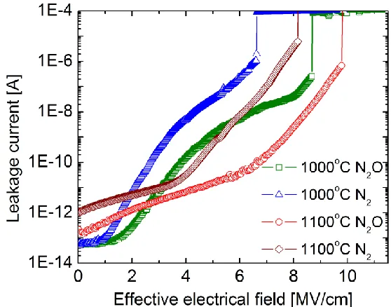
Figure 3.6. Gate leakage of 100 um*100 um capacitors with ALD SiO2 with 900 oC and 1000 oC N 2 PDA and thermal (dry O2) SiO2 grown at 900 oC. ... 55
Figure 3.7. XPS Si 2p spectra (taking off angle) for ALD received 900 oC or 1000 oC PDA in N2. ... 56
Figure 3.8. (a) C-V characteristics of MOS capacitors using 7 nm ALD ALD SiO2 with various PDA conditions (b) extracted VFB of ALD SiO2 capacitors after N2 and N2O PDA . 58 Figure 3.9. Gate leakage of 100 um*100 um capacitors with ALD SiO2 after N2 and N2O PDA... 58
Figure 3.10. XPS Si 2p (left) and O 1s (right) spectra of 3nm ALD SiO2 at 90o taking off angle. ... 59
Figure 3.11. Si 2p spectrum (90o taking off angle) of as cleaned SiC and 3nm ALD SiO2 on SiC... 60
Figure 3.13. 100k Hz C-V characteristics of 10 nm ALD SiO2 samples after 600oC PMA. .. 61
Figure 3.14. 100k Hz C-V characteristics of 10 nm ALD SiO2 capacitor samples after 750 oC
PMA. ... 62 Figure 3.15. 100k Hz C-V characteristics of 10 nm ALD SiO2 capacitor samples after 900 oC
PMA. ... 63 Figure 3.16. Flatband voltages of ALD SiO2 capacitors with different PDA and PMA
conditions. ... 64 Figure 3.17. Measured and de-convoluted XPS Si 2p spectra (30o takeoff angle) of 3 nm ALD SiO2 after 600 oC, 750 oC, and 900 oC N2 PDA. ... 65
Figure 3.18. O 1s energy loss spectra of 15 nm ALD SiO2 on 4H-SiC after 600 oC, 900 oC
and 1000 oC PDA in N2.. ... 66
Figure 3.19. Valence band spectra of 15 nm ALD SiO2 on SiC after 600 oC, 900 oC and 1000 oC PDA... 67
Figure 3.20. C-V characteristics of 30 nm ALD SiO2 after 900 oC N2O PDA and 400 oC
PMA. ... 69 Figure 3.21. C-V characteristics of 30 nm ALD SiO2 after N2O PDA and N2 PDA at 900 oC
and 400 oC PMA. ... 69 Figure 3.22. C-V characteristics of 30 nm ALD SiO2 after 1000 oC PDA in N2O and 400 oC
PMA. ... 70 Figure 3.23. C-V characteristics of 30 nm ALD SiO2 after 900 oC and 1000 oC PDA in N2O
and 400 oC PMA. ... 70 Figure 3.24. C-V characteristics of 30 nm ALD SiO2 after 1100 oC PDA in N2O and 400 oC
PMA. ... 71 Figure 3.25. C-V characteristics of 30 nm ALD SiO2 after 1100 oC PDA in N2O and N2 and
400 oC PMA. ... 71 Figure 3.26. Gate leakage of ALD SiO2 after PDA in N2O and N2 and 400 oC PMA. ... 72
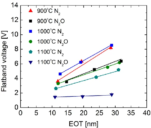
Figure 3.27. Interface states density near conduction band based on Hi-Lo C-V method. .... 73 Figure 3.28. VFB vs. EOT results and linear fitting of various MOS capacitors. ... 74
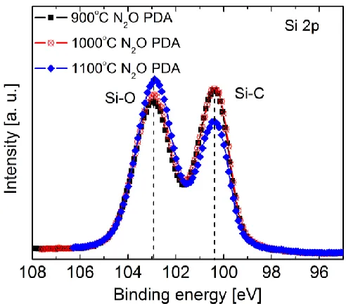
Figure 3.29. XPS Si 2p spectra (90o taking off angle) of 3 nm ALD SiO2 after 900 oC, 1000 oC, and 1100 oC PDA in N
2O. ... 75
Figure 3.30. XPS O 1s spectra (90o taking off angle) of 3 nm ALD SiO2 after 900 o C, 1000 o
C, and 1100 o C PDA in N2O. ... 76
Figure 3.31. XPS N 1s spectra (90o taking off angle) of 3nm ALD SiO
2 after 900 o C, 1000 o
C, and 1100 o C PDA in N2O. ... 77
Figure 3.32. O 1s energy loss spectra of 3nm ALD SiO2 on SiC after 900 oC, 1000 oC, and
Figure 3.33. 1M Hz C-V characteristics of capacitors with 13 nm Al2O3 using H2O and O3 as
the oxidizer after 600 oC PDA in N
2 and 400 oC PMA. ... 79
Figure 3.34. C-V characteristics of capacitors with 13 nm Al2O3 using H2O as the oxidizer
after 600 oC PDA in N2 and 400 oC PMA. ... 79
Figure 3.35. C-V characteristics of capacitor with 13 nm Al2O3 using O3 as the oxidizer after
600 oC PDA in N2 and 400 oC PMA. ... 80
Figure 3.36. C-V characteristics of Al2O3 capacitors using H2O and O3 as the oxidizer after
750 oC PDA in N2 and 400 oC PMA. ... 80
Figure 3.37. C-V characteristics of Al2O3 capacitors using H2O as the oxidizer after 750 oC
PDA in N2 and 400 oC PMA. ... 81
Figure 3.38. C-V characteristics of Al2O3 capacitors using O3 as the oxidizer after 750 oC
PDA in N2 and 400 oC PMA. ... 81
Figure 3.39. C-V characteristics measured at different measurement temperature from Al2O3
capacitors using H2O as the oxidizer after 600 oC PDA in N2 and 400 oC PMA. ... 82
Figure 3.40. C-V characteristics measured at different measurement temperature from Al2O3
capacitors using O3 as the oxidizer after 600 oC PDA in N2 and 400 oC PMA. ... 82
Figure 3.41. The flatband voltage results of Al2O3 capacitors on SiC with different PMA
conditions. ... 83 Figure 4.1. Flatband voltage vs. EOT results of single layer ALD SiO2 and Al2O3 on Si with
FGA. Both samples received N2 PDA at 900 oC. ... 88
Figure 4.2. Flatband voltage vs. EOT plot of dual-layer type 2 after 600 oC and 900 oC PDA. ... 89 Figure 4.3. Flatband voltage vs. EOT results of dual-layer type 1 and 2 on Si after after 600
oC and 900 oC PDA. ... 90
Figure 4.4. Theoretical prediction of the flatband voltage of alternating Al2O3 and SiO2 layers,
assuming no fixed charge anywhere. ... 92 Figure 4.5. Theoretical prediction of the flatband voltage of alternating Al2O3 and SiO2 layers
with neutralization layers (layer 3 and 6), assuming no fixed charge anywhere. ... 93 Figure 4.6. Flatband voltage and EOT results of single layer SiO2, SiO2/Al2O3,
SiO2/Al2O3/SiO2 and SiO2/Al2O3/SiO2/Al2O3. All samples received 900 oC PDA and 450 oC
FGA... 94 Figure 4.7. Flatband voltage and EOT results of of SiO2/Al2O3/SiO2, SiO2/Al2O3/SiO2/Al2O3,
and SiO2/Al2O3/HfO2/SiO2/ Al2O3. All samples received 900 oC PDA and 450 oC FGA. .... 95
Figure 4.8. C-V characteristics of dual-layer SiO2/Al2O3 after 600 oC and 750 oC PDA in N2
after 400 oC PMA. ... 96 Figure 4.9. C-V characteristics of dual-layer SiO2/Al2O3 after 600 oC and 750 oC PDA in N2
Figure 4.10. C-V characteristics of dual-layer 20 nm ALD SiO2/Al2O3 after 900 oC PDA in
N2O and 400 oC PMA . ... 98
Figure 4.11. 1M Hz C-Vs of dual-layer SiO2/Al2O3 and single layer ALD SiO2 after 900 oC
PDA in N2O and 400 oC PMA. ... 98
Figure 4.12. Flatband voltage against EOT results of ALD SiO2 and ALD SiO2/Al2O3
capacitors on SiC with 900 oC PDA in N2O and 400 oC PMA . ... 100
Figure 4.13. Flatband voltage vs. EOT results of ALD SiO2 and ALD SiO2/Al2O3 capacitors
on SiC with 1000 oC PDA in N2O and 400 oC PMA . ... 100
Figure 5.1. Schematic of fabricated lateral MOSFETs with ALD SiO2. ... 104
Figure 5.2. TLM results on N+ region from lateral MOSFETs samples. ... 105 Figure 5.3. Ids-Vgs characteristics of MOSFETs using 30 nm ALD SiO2 after 900 oC N2O
PDA... 105 Figure 5.4. Ids-Vgs characteristics of MOSFETs using 30 nm ALD SiO2 after 1000 oC N2O
PDA... 106 Figure 5.5. Ids-Vgs characteristics of MOSFETs using 30 nm ALD SiO2 after 1100 oC N2O
PDA... 107 Figure 5.6. Ids-Vds characteristics of MOSFETs using 30 nm ALD SiO2 after 1100 oC N2O
PDA... 108 Figure 5.7. Peak field effect mobility and VT of MOSFETs using ALD SiO2 as a function of
the N2O PDA temperature. ... 108
Figure 5.8. MOSFET characteristics using ALD SiO2 after 1000 oC N2 PDA. ... 109
Figure 5.9. Ids-Vgs characteristics of MOSFETs using the dual-layer stack and single layer
ALD SiO2 after 900 oC N2O PDA. ... 112
Figure 5.10. Subthreshold characteristics of MOSFETs using the dual-layer stack and single layer ALD SiO2 after 900 oC N2O PDA. ... 112
Figure 5.11. Field effect mobility of the MOSFET with the dual-layer stack after 900 oC N2O
PDA... 113 Figure 6.1. AFM image of Si face 4H-SiC after 60 s 1000 oC N
2O rapid thermal oxidation.
The scan size is 2 um*2 um. ... 115 Figure 6.2. C-V characteristics of MOS capacitor using 5.8 nm RTO after 400 oC PMA. .. 116 Figure 6.3. C-V characteristics of MOS capacitor using 1nm RTO covered with 20 nm ALD SiO2 with 900 oC N2 PDA and 400 oC PMA. ... 117
Figure 6.4. C-V characteristics of MOS capacitor using 1nm RTO covered with 20 nm ALD SiO2 with 900 oC N2O PDA and 400 oC PMA. ... 117
Figure 6.6. Interface states profile of ALD SiO2 after N2O PDA and capacitor with RTO
covered by 30nm ALD SiO2 after 900 oC N2O PDA... 119
Figure 6.7. 1M Hz C-V characteristics of MOS capacitors with and without RTO after 1000
oC N
2O PDA and 400 oC PMA. ... 119
Figure 6.8. I-V characteristics of MOS capacitors with and without RTO after 1000 oC N2O
PDA and 400 oC PMA. Both samples contain 30 nm ALD SiO2. ... 120
Figure 6.9. Ids-Vgs characteristics of MOSFETs with RTO covered by 30 nm ALD SiO2 after
900oC N2O PDA. ... 120
Figure 6.10. High gate bias normalized transconductance of MOSFETs using 1 nm RTO covered by 30 nm ALD SiO2 after 900 oC N2O PDA and the ALD SiO2 MOSFET with 1100 oC N
2O PDA. ... 122
Figure 6.11. MOS capacitor fabrication process with doped SiO2. ... 123
Figure 6.12. XPS spectra of SiO2 doped with nitrogen and phosphorus. ... 124
Figure 6.13. C-V characteristics of MOS capacitor using 4 nm SiO2 from sputtering (no
phosphorus or nitrogen) covered with 30nm ALD SiO2 with 900 oC N2O PDA and 400 oC
PMA. ... 125 Figure 6.14. C-V characteristics of MOS capacitor using nitrogen doped SiO2 from sputtering
covered with 30 nm ALD SiO2 with 900 oC N2O PDA and 400 oC PMA. ... 125
Figure 6.15. C-V characteristics of MOS capacitor using phosphorus doped 4 nm SiO2 from
sputtering covered with 30 nm ALD SiO2 with 900 oC N2O PDA and 400 oC PMA. ... 126
Figure 6.16. C-V characteristics of MOS capacitors with doped SiO2 and device with only
30nm ALD SiO2 .. ... 127
Figure 6.17. Interface states profile of ALD SiO2 after N2O PDA and capacitor with nitrogen
and phosphorus doped SiO2 covered by 30nm ALD SiO2 after 900 oC N2O PDA. ... 127
Figure 6.18. Ids-Vgs characteristics of MOSFETs using 4 nm phosphorus doped SiO2 by
sputtering covered by 30nm ALD SiO2 after 900oC N2O PDA. The Si layer is not sufficiently
oxidized. ... 128 Figure 6.19. Ids-Vgs characteristics of MOSFETs using 4 nm undoped SiO2 covered by 30 nm
ALD SiO2 after 900 oC N2O PDA. ... 128
Figure 6.20. Ids-Vgs characteristics of MOSFETs using 4 nm phosphorus doped SiO2 covered
by 30 nm ALD SiO2 after 900 oC N2O PDA. ... 129
Figure 6.21. Ids-Vgs characteristics of MOSFETs using 4 nm nitrogen doped SiO2 covered by
30 nm ALD SiO2 after 900 oC N2O PDA. ... 130
Figure 6.22. High field transconductance of MOSFETs using 4 nm phosphorus doped SiO2
covered by 30 nm ALD SiO2 after 900 oC N2O PDA and SiO2 MOSFET after 1100 oC N2O
Figure 6.23. High field transconductance of MOSFETs using 4 nm nitrogen doped SiO2
covered by 30 nm ALD SiO2 after 900 oC N2O PDA and SiO2 MOSFET after 1100 oC N2O
PDA... 131 Figure 6.24. SiC MOSFET benchmark with devices discussed in this chapter. ... 132 Figure 7.1. La 3d XPS spectra of LaSiOx/ SiO2 stackwith and without 900 oC N2O PDA. 136
Figure 7.2. O 1s XPS spectra of LaSiOx/ SiO2 stackwith and without 900 oC N2O PDA. .. 136
Figure 7.3. Schematic of fabricated MOS capacitor with LaSiOx. ... 137
Figure 7.4. C-V characteristics of MOS capacitors with LaSiOx after 900 oC N2O PDA. ... 138
Figure 7.5. 1M Hz C-V characteristics of capacitors with and without LaSiOx after 900 oC
N2O PDA. ... 138
Figure 7.6. C-V characteristics of MOS capacitors with LaSiOx after 1000 oC N2O PDA. . 139
Figure 7.7. 1M Hz C-V characteristics of MOS capacitors with LaSiOx after 900 oC and 1000 oC N
2O PDA. ... 139
Figure 7.8. I-V characteristics of capacitors with LaSiOx after 900 oC and 1000 oC N2O PDA
and ALD SiO2 sample with 1000 oC N2O PDA. ... 140
Figure 7.9. Dit profile extracted from MOS capacitors with LaSiOx after 900 oC and 1000 oC
N2O PDA and ALD SiO2 after 900 oC N2O PDA. ... 141
Figure 7.10. Z-contrast STEM image of ALD SiO2 on LaSiOx (900 oC N2O PDA). The bright
layer is the La rich layer. ... 142 Figure 7.11. Z-contrast STEM images of samples with (left) and without (right) LaSiOx. . 143
Figure 7.12. Intensity profiles taken from the Z-contrast STEM images in Fig. 7.11: (left) with LaSiOx and (right) without LaSiOx. ... 143
Figure 7.13. Schematic of fabricated MOSFET with LaSiOx. ... 144
Figure 7.14. Ids-Vgs characteristics of MOSFETs using LaSiOx covered by 30 nm ALD SiO2
after 900 oC N2O PDA. ... 145
Figure 7.15. Ids-Vds characteristics of MOSFETs using LaSiOx covered by 30 nm ALD SiO2
after 900 oC N2O PDA. ... 146
Figure 7.16. Ids-Vds characteristics of MOSFETs using LaSiOx covered by 30 nm ALD SiO2
after 900 oC N2O PDA and the ALD SiO2 MOSFET with 1100 oC N2O PDA. ... 146
Figure 7.17. Effective mobility of MOSFETs with LaSiOx after 900 oC N2O PDA. ... 147
Figure 7.18. Ids-Vgs characteristics of MOSFETs using LaSiOx covered by 30 nm ALD SiO2
after 1000 oC N2O PDA. ... 148
Figure 7.19. Peak mobility and VT of MOSFETs with LaSiOx as a function of the N2O PDA
temperature. ... 148 Figure 7.20. Subthreshold characteristics of MOSFETs with LaSiOx after PDA at various
Figure 7.21. Z-contrast STEM images of LaSiOx/SiO2 stack after 900 oC N2O PDA and 1100 oC N
2O PDA (insert). ... 150
Figure 7.22. MOSFET mobility dependence in La2O3 thickness (900 oC N2O PDA). ... 152
Figure 7.23. Threshold voltage as a function of La2O3 thickness (900 oC N2O PDA). ... 152
Figure 7.24. Subthreshold characteristics of MOSFETs with various initial La2O3 thicknesses
after 900 oC N2O PDA. ... 153
Figure 7.25. SiC MOSFET benchmark with devices discussed in this chapter. ... 155 Figure 8.1. Temperature dependence of mobility and VT measured from the ALD SiO2
MOSFET 1100 oC N2O PDA. ... 158
Figure 8.2. Temperature dependence of mobility and VT measured from the MOSFET with
RTO and 30 nm ALD SiO2 after 900 oC N2O PDA. ... 159
Figure 8.3. Temperature dependence of mobility and VT measured from MOSFET with
phosphorus doped SiO2 and 30 nm ALD SiO2 after 900 oC N2O PDA. ... 160
Figure 8.4. Temperature dependence of mobility and VT of MOSFET with LaSiOx after 900 oC N
2O PDA. ... 161
Figure 8.5. Temperature dependence of mobility and VT of MOSFETs with LaSiOx after N2O
PDA at various temperatures. ... 162 Figure 8.6. Temperature dependence of mobility of MOSFETs with LaSiOx with different
initial La2O3 thicknesses after 900 oC N2O PDA. ... 163
Figure 8.7. Gate voltage wave forms of the accumulative gate stressing. ... 164 Figure 8.8. VT shift after room temperature accumulative gate stressing at 3 MV/cm on ALD
SiO2 MOSFETs after 1000 oC and 1100 oC N2O PDA. ... 165
Figure 8.9. VT shift after room temperature accumulative gate stressing at different electrical
fields on ALD SiO2 MOSFETs after 1100 oC N2O PDA. ... 166
Figure 8.10. VT shift after room temperature accumulative gate stressing at 3 MV/cm on
ALD SiO2 MOSFETs after 1100 oC N2O PDA with recovery after stressing. ... 167
Figure 8.11. VT shift after room temperature accumulative gate stressing at 3 MV/cm on
MOSFETs using nitrogen and phosphorus doped SiO2 after 900 oC N2O PDA. ... 168
Figure 8.12. VT shift after room temperature accumulative gate stressing at 3 MV/cm on
MOSFETs with RTO after 900 oC N2O PDA. ... 168
Figure 8.13. VT shift after room temperature accumulative gate stressing at various electrical
fields on MOSFETs with LaSiOx and ALD SiO2 after 900 oC N2O PDA. ... 169
Figure 8.14. VT shift after room temperature accumulative gate stressing at 3 MV/cm on
MOSFETs with different initial La2O3 thicknesses. ... 170
Figure 8.15. VT shift after room temperature accumulative gate stressing at 3 MV/cm and
Figure 8.16. Field effect mobility curves of the 900 oC N2O PDA MOSFET with LaSiOx
Chapter 1
Review of 4H-SiC MOSFETs
In this chapter, 4H-SiC material properties and its potential applications for power
electronics will be briefly reviewed. Subsequently, the introduction will focus on efforts to
improve 4H-SiC MOSFET mobility.
1.1 Overview of SiC and devices
Table 1.1. Material properties of most common SiC polytypes [1, 2, 3].
Polytype 4H 6H 3C
Crystal structure
Wurtzite Wurtzite Zinc Blended Bandgap [eV]
3.24 3.03 2.2
Electron affinity [eV]
3.1 3.3 3.8
Bulk Mobility [cm2/V · s]
720-900 370 1000
Critical field 106 [V/cm]
3 2.3-2.4 1.5
Thermal conductivity 300K [W/cm · K]
In the past two decades, Silicon Carbide (SiC) based power devices have attracted
significant research interest, due to superior electrical properties of SiC, especially for 4H
and 6H SiC polytypes [1-3]. As shown in Table 1, these properties include wide bandgap,
high critical electrical field and good thermal conductivity.
The polytypes are determined by Si-C atomic arrangement and stacking sequence in the
<0001> direction of the crystal. Among the common SiC polytypes, 4H-SiC is considered to
be the most promising one due to its wider bandgap and higher bulk mobility compared to
the other polytypes. The materials properties of Si, 4H-SiC and Wurtzite GaN are listed in
Table 2.
Si based power Metal Oxide Semiconductor Field Effect Transistors (MOSFETs), Insulated
Gate Bipolar Transistor (IGBT), and Thyristors are the dominant power switching devices in
the market today. Both SiC and GaN based devices are promising post silicon power
switching devices due to its wider bandgap and significantly higher breakdown electrical
field than Si, further materials optimization is necessary to achieve the ultra high voltage
operation.
Table 2 also compares various figures of merits of the three semiconductors: the Baliga's
Figure of Merit (BFOM) represents the on state resistive loss; BHFFOM is Baliga's High
Frequency Figure of Merit representing switching loss; HTFOM is the Thermal Figure of
Merit for thermal handling capability and CFOM is Combined Figure of Merit for overall
Table 1.2. Material properties of Si, 4H-SiC and Wurtzite GaN [7, 8].
Material Si SiC-4H GaN
Bandgap [eV] 1.12 3.24 3.42
Relative dielectric constant 11.7 9.7 9
Electron mobility [cm2/V*s] 1360 720-900 1200 (Bulk)
1300-2000 (2DEG)
Saturation velocity [107cm/s] 1.0 2.0 2.5
Critical field [MV/cm] 0.3 2.2-3 2.3-3.3
BFOM normalized to Si 1 220-440 200-900 (bulk)
BHFFOM normalized to Si 1 45 36-98
Thermal conductivity 300K [W/cm*K]
1.3 4.5 1.2
HTFOM normalized to Si 1 0.6 0.1
Figure 1.1. Si power devices selection depending on power rating and frequency. The boundaries are not strictly defined.
Figure 1.2. Applications of power devices selection depending on blocking voltage and current. The boundaries are not strictly defined.
Both 4H-SiC and GaN show superior material properties than Si for power switching
application and thus it is expected that in the future, the two materials will compete for
power or breakdown voltage (BV) above 1200V, SiC based devices have more advantages
due to the materials limitations of GaN.
At the present time, other than diodes, limited amounts of SiC based switching devices are
commercially available in the market, such as Double Diffusion MOSFETs (DMOSFETs)
and Junction Gate Field Effect Transistors (JFETs) from various companies. This section will
focus on process optimization of SiC lateral MOS devices.
Although MOSFETs on 4H-SiC have been studied for decades, the typical channel mobility
achieved for n-channel devices is significantly lower than the bulk mobility. Hence, the
primary goal of research activities in SiC MOS field continues to focus on improving the
electron mobility.
It is necessary to understand the source of these defects and improve fabrication process to
eliminate them. In addition to mobility enhancement, high enough threshold voltage (>3 V)
is also critical operation for power devices and thus any mobility enhancement must also be
commensurate with high threshold voltages.
The inversion mobility of 4H-SiC MOS devices remains extremely low compare to the bulk
mobility. To date, the dominant gate dielectric material of SiC MOS devices is thermally
grown SiO2. Although SiC has the advantage of being able to grow high quality SiO2 by
direct thermal oxidation, removal of carbon atoms from the substrate during the oxidation
remains challenging. The primary reason for low SiC MOSFET mobility is the high interface
states (Dit) near the conduction band, which are attributed to dangling silicon bands and
carbon related defects formed during high temperature oxidation [9-11]. Specifically, these
interface defects are combinations of near interface traps, dangling Si bonds at the SiC/oxide
interface (Pb centers), trivalent Si defects in the oxide (E' centers), Si-C-O bonds, and various
carbon interstitials [11-14]. As shown in Fig. 1.3, these defects are classified into three types:
near interface traps, carbon clusters and dangling Si bonds. The near interface states capture
electrons and become coulomb scattering centers, which severely reduce the inversion
mobility. Typical near interface states at 4H-SiC/SiO2 interface in the upper band gap are
acceptor-like traps, which are negatively charged when electrons are trapped by these traps
[9]. The structural of silicon face (0001) 4H-SiC /SiO2 interface is believed to lead to high
density of dangling SiC bonds, which can be passivated by hydrogen anneals. In literature,
compared to the overall interface states, and thus hydrogen anneals have minimal effect on
mobility. However, the dangling bonds may have stronger impact on devices using deposited
oxides.
The carbon related defects are formed during oxidation when there is not sufficient oxygen to
oxidize carbon into CO or CO2 and subsequently be released [12]. Researchers have
proposed that the presence of high concentration of C atoms in the substrate in the form of
carbon single interstitials (Ci) have a 0.5-1.4eV migration barrier height in the 4H-SiC lattice
[13]. Others have proposed clustered carbons explanations [14]. The most commonly
reported cluster is the carbon di-interstitial, or (Ci)2 [14]. (Ci)2 can bond to the lattice by the
double C-C bond and two C-Si bonds. This cluster has a migration barrier as high as 5-6eV
and therefore it is stable in the lattice. After examining the energy levels of (Ci)2 in SiC
bandgap, Devynck et al. claim that the cluster is negatively charged in n-type SiC with energy levels close to the conduction band edge (Ec-0.04 eV or Ec-0.23 eV) and positively
charged in p-type at 0.49 eV or 0.71 eV from the valence band edge [13]. In either case, the
charged defects act as the coulomb scattering centers, especially for the ones located in the
vicinity of conduction band.
Other than the above mentioned defects associated with thermal oxide or SiC/oxide interface,
the crystal defects in the SiC epitaxial layer also effect the device overall performance. Point
defects created or propagated during epitaxial growth and defects formed during high
temperature annealing process, such as phosphorus dopant activation anneal at 1650oC, are
carrier lifetime killers and thus negatively impact SiC diode performance [15]. As far as
MOSFET inversion mobility is concerned, the shallower traps have stronger influence on the
mobility than the deep levels. In addition, the major SiC defects such as down-falls, carrots,
triangular defects, and micropipes are extremely detrimental to device operations but these
defects can be eliminated with improved crystal growth technology [9].
Finally, the surface roughness of 4H-SiC wafers should not be ignored due to off c-axis
cutting of typical commercially available 4H-SiC wafers. To avoid cubic SiC phases
inclusions in the 4H-SiC crystal during epitaxial growth, the substrate are cut as high as 8o
off the c-axis toward <11-20> direction. The state-of-the-art MOSFETs fabricated on lower
angle off-axis Si-face substrates do not show higher peak mobility than the ones on higher
angle off-axis wafers [16]. However, with improved mobility, the surface roughness could
have a strong impact on the peak mobility and the mobility at higher electrical field.
Devices fabricated on different faces of 4H-SiC have also been studied [17-19]. The
carbon-face (000-1) of 4H-SiC is known to create challenges to control the doping in the epitaxial
layer and contains higher interface states density after oxidation than the silicon-face [17].
Devices built on the a-face (11-20) show promising mobility results and thinner interfacial
layer [18, 19]. The progresses on a-face will be discussed in this chapter. The device
properties require further investigation for potential applications and the quality and
availability of such substrates must be improved. Therefore, in this work, the literature
In summary, it is commonly believed various defects associated with high temperature
thermal oxidation are the culprit of low electron mobility.
1.2 Mechanisms of Mobility Degradation
From a device physics point of view, the mobility degradation mechanism can be
modeled as a combination various carrier scattering processes, including coulomb, surface
roughness, and phonon scattering processes. These scattering mechanisms have different
dependences on temperature and electrical field, and therefore modeling can be performed to
fit the experimental data and evaluate the contribution of each component. Furthermore, the
bulk mobility also limits the device mobility when the mobility is or the measurement
temperature high enough. However, at the present, the bulk mobility is significantly higher
than the other mobility components at measurement temperature from room temperature to
highest proposed operating temperature for 4H-SiC devices.
Based on Mathiessen’s rule, the total low field mobility is inversely proportional to the sum
of the individual mobility terms. The total low field mobility can be written as:
μB, μC, μph and μsr are mobility terms determined by bulk mobility, coulomb scattering,
The bulk SiC mobility along the c-axis is:
where μmax (500 cm2/V*s) is the maximum low-filed bulk mobility [20]. ηB, γB and Nref are
parameters from simulations and experimental results [20]. At room temperature (300K), the
bulk 4H-SiC mobility is significantly higher than any other mobility component.
The mobility component related to acoustic phonon scattering is given by the following
equation:
where h is the Planck's constant, ρs is the areal density of SiC, ul is the sound velocity in SiC,
m* is the density of states effective mass, mc is the conductivity effective mass, ZA the
surface phonon deformation potential, and kB is the Boltzmann's constant, respectively.
The mobility results from coulomb interactions from fixed oxide charge and trapped interface
states are given by:
where εox is the permittivity of gate oxide, εSiC is the permittivity of SiC, NT is the sum of all
is the surface electron density, n0 is a proportionality factor, and ζ is an empirical parameters
(0.5).
The low field mobility component limited by surface roughness scattering, which is a
complicated phenomenon for oxide on SiC, is given by:
where δsr is a constant related to interface properties, and E┴is perpendicular electrical field.
The temperature dependences of the low field mobility components are listed in Table.3.
From the table, only the mobility determined by coulomb scattering (μc), which was induced
by fixed charges and Dit, increases with device operating temperature. Bulk mobility and
phonon mobility decreases with the operating temperature. Surface roughness mobility does
not have an explicit dependence on temperature. Since the lowest one dominates the total
mobility, we can determine the dominant term by studying the temperature dependence of the
MOSFET mobility.
Table 1.3. Temperature dependence of four mobility components [20].
μB μC μph μsr
Due to high density of interface states, which are known coulomb scattering centers, the total
low field mobility of thermal SiO2 based MOSFETs is limited by the coulomb mobility [20].
Even state-of-the-art nitric oxide (NO) anneal reduces the interface states density and total
effective charge density at SiC/SiO2 interface, the mobility is still limited by coulomb
scattering [20]. When the mobility is further improved, the effect of acoustic phonon and
surface roughness scattering should be more pronounced.
Based on modeling, the effect of surface roughness scattering is believed to affect the
mobility at relatively higher electrical field. The roughness of SiC surface may include the
roughness caused by oxidation or high temperature anneals, as well as the inherent roughness
due to off-axis cut. Dhar et al. have performed mobility modeling with experimental Hall mobility results of thermal SiO2 and deposited SiO2 with NO anneal. While many electron
mobility measurements can be performed, Hall mobility directly represents the carrier
transportation process [11]. They have compared the Hall mobility of thermal grown and
deposited SiO2 after NO anneal. For both thermal and deposited SiO2, measured Hall
mobility data points agree well with the coulomb mobility model at low electrical field or
gate voltage. As expected, for thermal SiO2, the measured values start to depart from the
coulomb mobility model at around 10 V and a combined model of coulomb mobility and
surface roughness model gives a more accurate fitting. This result generally agrees with other
reported thermal SiO2 mobility degradation analysis, i.e. the coulomb scattering dominates at
the low field and the effect of surface roughness may emerge at higher field [11]. For
indicating that the mobility is not limited by surface roughness scattering. The result suggests
the surface roughness may have a profound impact on the mobility at relatively higher field
and its influence highly depends on the process.
Although the hall mobility is more suitable to study electron transportation mechanisms, the
field effect mobility and effective mobility, measured from MOSFETs are more commonly
used as the figure-of-merit for a given SiC MOS technology. In this work, the mobility
results discussed will be the field effect mobility (μFE), which is extracted from the
transconductance of Ids-Vgs characteristics.
In summary, it is widely reported that mobility degradation of 4H-SiC MOSFETs is mainly
due to coulomb scattering of high density interface states. At high electrical field, surface
roughness caused by the oxidation can be a significant mobility limiting mechanism.
1.3 Mobility Enhancement: Nitridation
In this section, efforts to improve channel mobility of SiC MOSFETs using
nitridation will be reviewed. All the results are from the Si-face of SiC n-channel lateral
MOSFETs unless specified otherwise.
Since 1996, nitridation of SiO2 have been the state-of-the-art technique to improve the
mobility of SiC MOSFETs. Nitrogen can be introduced into SiO2 or at the SiO2/SiC interface
and ammonia (NH3). It is preferred to introduce nitrogen at the interface and passivates
carbon related defects, instead of incorporating nitrogen throughout the oxide. For various
reasons, after nitridation, the measured interface states density is found to be greatly reduced.
NO treatment is the most effective nitridation method for the following reasons: NO anneal
can introduce nitrogen to the oxide and nitrogen species becomes concentrated at the
oxide/SiC interface; N2O anneal incorporates less amount of nitrogen and also tends to
oxidize the substrate more than NO at a given temperature, which create defects similar to
standard oxidation processes in dry O2 [22]; NH3 anneal leaves a relatively large amount of
nitrogen throughout the oxide and converts the dielectric to an SiOxNy layer, with nitrogen to
oxygen ratio as high as 1:1.5 [23]. Large amount of nitrogen incorporation in the bulk of the
SiO2 leads to undesirable properties of silicon nitride (SiN), such as higher gate leakage,
trapping and reliability degradation.
As an alternative way to introduce nitrogen into the SiC and at the dielectric-semiconductor
interface, low dose nitrogen implantation in the channel before oxide formation can also be
used to achieve nitrogen passivation. With the nitrogen dose of 8E12 cm-2 at 50 keV, the
peak mobility was dramatically improved to 99 cm2/Vs [24]. However, the threshold voltage
became negative with higher nitrogen implantation dose. The authors proposed that the band
bending or counter-doping caused by the nitrogen implantation could turn the SiC surface
n-type and thus the inversion layer would be formed in the substrate, instead of in the defect
rich layer near SiC/SiO2. Due to the unique band structure, this technique is also called
enhancement may also due to prevention of carbon clusters by the nitrogen atoms in the
substrate [24].
The major issue associated with the implantation technique is the negative threshold voltage
shift and the dramatic reduction of mobility when it passes its peak. While the peak mobility
is normally reported as figure-of-metric for MOSFET performance, mobility at higher gate
bias is more important for power devices since they are typically biased a few volts above the
threshold (gate overdrive).
There are other methods to introduce nitrogen into the interface or substrate, including SiN
deposition [25], nitrogen atomic source treatment [26] and nitrogen plasma irradiation [27].
These processes have not been proven to significantly improve the mobility and require
further optimization. The fundamental issue with nitrogen related techniques is the threshold
voltage control, because mobility improvement via nitrogen incorporation is typically
associated with significantly lowered threshold voltage, due to presence of the positively
charged nitrogen species.
Other annealing techniques have been studied to improve the device performance, such as
hydrogen treatment or the forming gas anneal (FGA) [28]. Low temperature hydrogen anneal
is proven to be ineffective to High temperature anneal of thermal SiO2 in H2 produces a
1.4 Mobility Enhancement: Phosphorus Treatment
In recent years, phosphorus (P) passivation of defects at SiC/SiO2 has been studied to
improve the mobility. Okamoto et al. developed a phosphoryl chloride (POCl3) anneal
process to introduce phosphorus to the SiC/thermal oxide interface [29]. POCl3 anneal
dramatically improve the electrical properties of thermal SiO2 on 4H-SiC. The interface
states density was further reduced by POCl3 anneal, compared to NO annealed samples [29].
The Dit value is reduced by more than one order of magnitude after a 1000 oC POCl3 anneal
[29]. In addition, the mobility is improved compared to a typical NO anneal. They reported
90 cm2/Vs peak mobility, compared to 50 cm2/V*s from typical NO anneal.
As a more convenient method, annealing of samples in the vicinity of a planar phosphorus
diffusion source can also be used to introduce phosphorus into the oxide [30]. This process
has been used to dope Si using traditional diffusion tube processes. After the annealing, SiO2
is converted to Phosphorous Glass (PSG). This technique gives similar results to POCl3
anneal and it can be achieved without POCl3 bubbler.
Nitrogen and phosphorus are n-type dopants for SiC. In n-channel MOSFETs, if these n-type
dopants species diffuse into the p-type substrate, they may reduce the substrate doping level
and even invert the p-type SiC into near the surface. Medium energy ion spectroscopy
(MEIS) data show that, after typical NO and phosphorus anneal, nitrogen or phosphorus
Both nitrogen and phosphorus incorporation can be explained by the counter doping
hypothesis. If the counter doping level is enough to invert the substrate into n-type, the
MOSFETs become buried channel devices. This phenomenon resembles the effect of the
nitrogen implantation but the counter doping only occurs in an extremely thin layer near the
surface.
However, similar to nitrogen passivation, while phosphorus related process can enhance the
mobility, it degrades the threshold voltage due to the positive charge related to phosphorus
[29]. Also, while well optimized NO anneal improves MOSFET reliability, phosphorus in
SiO2 leads to serious device VT instability [32]. To alleviate the severe VT instability issue
due to trapping in bulk PSG, thinner PSG layer covered by thick deposited oxide has been
investigated in search for the trade-off between mobility and reliability [32]. However, when
the PSG layer is thinner than 10nm, the mobility enhancement is significantly undermined
[32].
1.5 Mobility Enhancement: Group1 Metal Ions Incorporation
Allerstam et al. reported enhanced oxidation rate of SiC in the presence of sintered alumina equipments, which contain sodium ions (Na+) [33]. They claim that sodium ions
enhance the oxidation rate and reduce the Dit compared to the sodium free samples [33].
Although the sodium ions, which are mobile charges in SiO2, can seriously degrade the
Since sodium mobility enhancement was reported, the effect of Potassium, Cesium and
Rubium has also been studied for mobility enhancement [34, 35]. Similar Dit reduction is
observed for most Alkali metal ions. Tuttle et al. provided a systematic explanation of the effect of sodium [34]. Based on their theory, sodium ions do not passivate dangling bonds,
carbon related defects or near interface traps. High concentration sodium ions may produce
large amount of shallow donor levels near SiC conduction band. These conducting donor
levels affect the movement of the Fermi level and, as a result, the high density traps near the
conduction band are skipped. Therefore, these ions do not reduce the actual interface state
density but the amount of interface states captured by typical C-V based measurement is
lowered.
Since sodium ions are well-known mobile charges in SiO2, any process containing sodium or
other Group 1 metal ions can hardly be applied in practice due to severe reliability
degradation, especially VT instability. The studies of Alkali ions enhancement are mainly
carried out for the understanding of mobility degradation of SiC MOS devices.
1.6 Mobility Enhancement: Deposited Dielectrics
Due to the issues associated with thermal oxide, deposited oxides on SiC have been
extensively studied as alternatives to thermal oxide. Since SiO2 is the most probable gate
dielectrics for SiC MOS devices for power applications, SiO2 deposited by various
Chemical Vapor Deposition (LPCVD) process [36]. With the same nitridation treatment,
LPCVD SiO2 shows higher peak mobility than thermal SiO2. They compared the results of
LPCVD thermal SiO2 after NO nitridation, thermal SiO2 after N2O anneal and as oxidized
SiO2. LPCVD oxide with NO nitridation gives the highest mobility [36].
Noborio et al. studied the properties of SiN deposited by Plasma Enhanced Chemical Vapor Deposition (PECVD) [25]. They showed N2O annealed PECVD SiO2 can give a mobility of
26 cm2/Vs, which is lower than typical results from NO annealed thermal SiO2.
Kim et al. demonstrated MOSFET results using SiO2 by Atomic Layer Deposition (ALD)
[32]. The ALD deposition was performed at 310 oC using Bis(diethylamino)silane and ozone
(O3) as the precursors. They claim that, since no oxidation is performed, ALD SiO2 contains
less carbon content than typical thermal oxide because there is no carbon atom released from
the substrate. They compared the MOSFET results of NO annealed ALD SiO2 and thermal
oxide. With similar peak field effect mobility, ALD SiO2 on SiC shows sharply lower
interface state density near the conduction band edge than thermal oxide device. Although
peak mobility enhancement is not obvious, ALD SiO2 samples maintain higher mobility at
high electrical field than the thermal oxide device, which is potentially due to lower SiC
surface roughness without high temperature thermal oxidation [32]. The high field mobility
result largely agrees with other reports using deposited oxide results, indicating deposited
S. Haney also studied ALD SiO2 using a low temperature recipe [16]. This ALD process
utilizes self catalyzed hydrolysis of 3-aminopropyltriethoxysilane (3-APTS) by H2O and O3
at 150 oC substrate temperature. With NO anneal, similar peak field effect mobility as
thermal oxide based devices was observed. After the same NO anneal, the amount of
nitrogen incorporated into the ALD SiO2 was higher compared to that of the thermal oxide.
Deposited SiO2 based MOSFETs show promising mobility results but no clear advantage
over thermal oxide has been demonstrated. Although they are unlikely to be used as the main
gate dielectrics of power MOSFETs, high-k dielectrics have also studied on 4H-SiC [38, 39]. Hino et al. reported results of MOCVD Al2O3 on SiC and Al2O3 on thin thermal SiO2 [38].
They demonstrated mobility results of MOCVD Al2O3 deposited at 190 oC and 230 oC. The
190 oC Al2O3 showed much higher mobility than the 230 oC sample. On the other set of
experiments, they studied MOCVD Al2O3 on thin thermal oxide. High field effect mobility
value (284 cm2/Vs) was achieved for their device with 190 oC Al
2O3 on thin thermal oxide
stack. It is noted the results were achieved using a gate last fabrication process and the high
mobility has not been shown by other groups using similar processes.
1.7 Progress of 4H-SiC MOSFETs on other faces
Non-polar 4H-SiC faces, such as the a-face (11-20), are known to show considerably
different material properties from polar faces, such as Si-face and C-face [18]. Much lower
non-polar nature and lower dangling bond density. 70-200 cm2/Vs peak field effect mobility has
been demonstrated using NO anneal, which is greatly higher than the Si-face or C-face
results [18]. High temperature (800 oC) H
2 anneal is proven to be very effective to improve
the mobility of thermal oxide based MOSFETs on a-face [19]. The bandgap, critical
electrical field and thermal conductivity of a-face substrates are supposed to be lower than
those parameters of Si-face and not well-known.
1.8 Research goals and tasks
The goal of this research project is to design a novel gate stack for Si-face 4H-SiC
MOSFETs using ALD deposited gate dielectrics. SiO2 deposited by ALD is selected as the
main to avoid the carbon related defects caused by thermal oxidation and suppress the gate
leakage given its large conduction band offset to SiC. Using deposited oxide also enables
interface engineering to independently control the interface properties.
The primary goal is to achieve high MOSFET peak field effect mobility (> 100 cm2/Vs) on
Si-face using ALD dielectrics and various interface engineering techniques. The electrical
properties of ALD SiO2 (using 3-APTS, H2O, and O3) will be systematically studied first.
The other objective of the project is to explore the VT enhancement using the SiO2/Al2O3
dipole effect. Experiments will be carried out to verify the dipole effect on SiC substrate
using the SiO2/Al2O3 stack deposited by ALD and study the possibility of stacking the
1.9 Summary of the Introduction
Figure 1.4. Mobility vs. threshold plot for typical reported techniques. Courtesy of S. Haney and Cree Inc. [16, 23-39].
In summary, typical reported mobility, threshold voltage and Dit results of lateral MOSFETS
4H-SiC are listed in Table 1.4 and plotted in Fig. 1.4. Fig. 1.4 shows that high mobility
results coincide with low threshold voltages. This observation is known as the trade-off
between mobility and threshold voltage. This trade-off has been proven for NO annealed
thermal SiO2 systems. The blue data points in Fig. 1.4 are based on Cree's thermal oxide data.
The blue data points and trend line clearly show that the mobility can be improved at the cost
of threshold voltage due to the positive charges introduced by NO anneals. For example,
observed for other techniques, as indicated by the red data points in Fig. 1.4. Therefore, the
major challenge in this field is to break the trade-off between mobility and threshold voltage.
1.10 References
[1]M. Shur, S. Rumyanstev, M. Levinshtein, SiC Materials and Devices, World Scientific, Singapore, 2006.
[2]Y.S. Park, R.K. Willardson, E.R. Weber, SiC Materials and Devices, Semiconductors and Semimetal, vol. 52, Academic Press, San Diego, CA, 1998.
[3]G. L. Harris, Properties of Silicon Carbide, Inspec publication, London, 1995.
[4]B. J. Baliga, “Power semiconductor device figure of merit for high – frequency applications,” IEEE Electron Device Lett., vol. 10, pp. 455–457, 1989.
[5]E. O. Johnson, “Physical Limitations on Frequency and Power Parameters of Transistors,” RCA Rev., pp. 163–177, 1965.
[6]A. Q. Huang, “New Unipolar Switching Power Device Figures of Merit,” IEEE Electron Device Lett., vol. 25, no. 5, pp. 455–457, 2004.
[7]U. K. Mishra, P. Parikh and Y.-F. Wu, “AlGaN/GaN HEMTs-an overview of device operation and applications,” Proc. IEEE, vol. 90, no. 6, pp. 1022−1031, 2002.
[9]G. Pensl, S. Beljakowa, T. Frank, K. Gao, F. Speck, T. Seyller, L. Ley, F. Ciobanu, V. Afanas'ev, A. Stesmans, T. Kimoto, and A. Schöner, “Alternative techniques to reduce inteface traps in n-type 4H-SiC MOS capacitors,”Phys. Stat. Sol. (b), vol. 245, no. 7, pp. 1378–1389, 2008.
[10]T. Zheleva, A. Lelis, G. Duscher, F. Liu, I. Levin, and M. Das, “Transition layers at the SiO2/SiC interface,” Appl. Phys. Lett., vol. 93, pp. 022108, 2008.
[11]S. Wang, M. Di Ventra, S. G. Kim, and S. T. Pantelides, “Atomic-Scale Dynamics of the Formation and Dissolution of Carbon Clusters in SiO2,” Phys. Rev. Lett., vol. 86, pp. 5946, 2001.
[12]S. Dhar, S. Haney, L. Cheng, S. R. Ryu, A.K. Agarwal, L.C. Yu and K. P. Cheung, “Inversion layer carrier concentration and mobility in 4H-SiC metal-oxide-semiconductor field-effect transistors,” J. Appl. Phys., vol.108, pp. 054509, 2010.
[13]N. H. Thoan,K. Keunen, V. V. Afanas’ev, and A. Stesmans, “Interface state energy distribution and Pb defects at Si(110)/SiO2 interfaces: Comparison to (111) and (100) silicon orientations,” J. Appl. Phys., vol. 109, pp. 013710, 2011.
[14]F. Devynck, A. Alkauskas, P. Broqvist, and A. Pasquarello, “Energy levels of candidate defects at SiC/SiO2 interfaces” AIP Conf. Proc., vol. 1199, pp. 108, 2010.
[15]X. Shen and S.T. Pantelides, “Identification of a major cause of endemically poor mobilities in SiC/SiO2 structures” Appl. Phys. Lett., vol. 98, pp. 053507, 2011.
[16]S. K. Haney, “Investigation of low temperature, atomic-layer-deposited oxides on 4H-SiC and their effect on the 4H-SiC/SiO2 interface”, Ph.D thesis, NCSU, Raleigh NC, 2012.
[18]H. Yano, T. Hirao, T. Kimoto, H. Matsunami, K. Asano, and Y. Sugawara, “High channel mobility in inversion layers of 4H-SiC MOSFETs by utilizing (11-20) face,” IEEE Electron Device Lett., vol. 20, no. 12, pp. 611– 613, 1999.
[19]J. Senzaki, K. Kojima, S. Harada, R. Kosugi, S. Suzuki, T. Suzuki, K. Fukuda, “Excellent effects of hydrogen postoxidation annealing on inversion channel mobility of 4H-SiC MOSFET fabricated on (11-20) face,” Electron Device Lett., vol. 23, no.1, pp. 13-15, 2002.
[20]S. K. Powell, N. Goldsman, J. M. McGarrity, J. Bernstein, C. J. Scozzie, and A. Lelis, “Physics-based numerical modeling and characterization of 6H-silicon-carbide metal– oxide–semiconductor field-effect transistors,” J. Appl. Phys., vol. 92, no. 7, pp. 4053– 4061, 2002.
[21]S. Potbhare, N. Goldsman, G. Pennington, A. Lelis, and J. M. McGarrity, “Numerical and experimental characterization of 4H-silicon carbide lateral metal-oxide-semiconductor field-effect transistor, ” J. Appl. Phys., vol. 100, pp. 044515, 2006.
[22]K. McDonald, M. B. Huang, R. A. Weller, L. C. Fedman, J. R. Williams, F. C. Stedile, I. J. R. Baumvol, and C. Radtke, “Comparison of nitrogen incorporation in SiO2/SiC and SiO2/Si structures,” Appl. Phys. Lett., vol. 76, pp.568, 2000.
[23]G. Chung, C. C. Tin, J. R. Williams, K. McDonald, M. Di Ventra, R. K. Chanana, S. T. Pantelides, L. C. Feldman, R. A. Weller, “Effects of anneals in ammonia on the interface trap density near the band edges in 4H–silicon carbide metal-oxide-semiconductor capacitors,” Appl. Phys. Lett., vol. 77, pp. 3601, 2000.
[24]S. Dhar, S.-H. Ryu and A. K. Agarwal, “A study on pre-oxidation nitrogen implantation for the improvement of channel mobility in 4H-SiC MOSFETs,” IEEE Trans. Electron Devices, vol.57, no. 6, 2010.
[26]J. W. Chai, J. S. Pan, Z. Zhang, S. J. Wang, Q. Chen, and C. H. A. Huan, “X-ray photoelectron spectroscopy studies of nitridation on 4H-SiC(0001) surface by direct nitrogen atomic source,” Appl. Phys. Lett., vol. 92, pp. 092119, 2008.
[27]H. Yang, D. Wang and H. Nakashima, “Significant Improvement of SiO2/4H-SiC Interface Properties by Electron Cyclotron Resonance Nitrogen Plasma Irradiation,” J. Electrochem. Soc., vol. 159, H1-H4, 2010.
[28]K. Fukuda, S. Suzuki and T. Tanaka, “Reduction of interface-state density in 4H–SiC n-type metal–oxide–semiconductor structures using high-temperature hydrogen annealing,” Appl. Phys. Lett., vol. 76, pp. 1585, 2000.
[29]D. Okamoto, H. Yano, K. Hirata, T. Hatayama, and T. Fuyuki, “Improved inversion channel mobility in 4H-SiC MOSFETs on Si face utilizing phosphorus-doped gate oxide,” IEEE Electron Device Lett., vol. 31, pp. 710, 2010.
[30]Y. K. Sharma, A. C. Ahyi, T. Isaacs-Smith, X. Shen, S. T. Pantelides, X. Zhu, L. C. Feldman, J. Rozen, and J. R. Williams, “Phosphorous passivation of the SiO2/4H-SiC interface,” Solid-State Electron, vol. 68, pp. 103-107, 2012.
[31]G. Liu, A. C. Ahyi, Y. Xu, T. Isaacs-Smith, Y. K. Sharma, J. R. Williams, L.C. Feldman, and S. Dhar, “Enhanced inversion mobility on 4H-SiC (11-20) using phosphorus and nitrogen interface passivation,” IEEE Electron Device Lett., vol. 34, no. 2, pp. 181-183, 2013.
[32]Y.K. Sharma, A.C. Ahyi, T. Isaacs-Smith, A. Modic, M. Park, Y. Xu, E. L. Garfunkel, S. Dhar, L. C.Feldman, J. R. Williams, “High-Mobility Stable 4H-SiC MOSFETs Using a Thin PSG Interfacial Passivation Layer,” IEEE Electron Device Lett., vol. 34, no. 2, pp. 175- 177, 2013.
[34]B. R. Tuttle, S. Dhar, S.-H. Ryu, X. Zhu, J. R. Williams, L. C. Feldman, and S. T. Pantelides, “High electron mobility due to sodium ions in the gate oxide of SiC-metal-oxide-semiconductor field-effect transistors,” J. Appl. Phys., vol. 109, pp. 023702, 2011.
[35]P. G. Hermannsson and E. Ö. Sveinbjörnsson, “Strong reduction in the density of interface states at the SiO2/4H-SiC interface after oxidation in the presence of alkali ions,” Phys. Scr., T148, pp. 014004, 2012.
[36]M. K. Das, “Recent advances in (0001) 4H-SiC MOS device technology,” Mat. Sci. Forum, vol. 457-460, pp. 1275-1280, 2004.
[37]C. Kim, J. H. Moon, J. H. Yim, D. H. Lee and J. H. Lee, “Comparison of thermal and atomic-layer-deposited oxides on 4H-SiC after post-oxidation-annealing in nitric oxide,” Appl. Phys. Lett., vol. 100, pp. 082112, 2012.
[38]S. Hino, T. Hatayama, J. Kato, E. Tokumitsu, N. Miura, and T. Oomori, “High channel mobility 4H-SiC metal-oxide-semiconductor field-effect transistor with low temperature metal-organic chemical-vapor deposition grown Al2O3 gate insulator,” Appl. Phys. Lett., vol. 92, pp. 183503, 2008.
Chapter 2
Experimental Procedures and Methodology
This chapter discusses the devices used in this work and the device fabrication
process flow. The processes for dielectrics and metals are described in details. Various
electrical and material characterizations techniques are reviewed.
2.1 Device structures
In this work, metal oxide semiconductor (MOS) or metal insulator semiconductor
(MIS) capacitors and lateral MOSFETs were fabricated and characterized to investigate the
properties of ALD dielectrics on 4H-SiC. MOS capacitors are the most simple device
structure which contains the substrate, the oxide layer and the gate electrode. The schematic
of a typical MOS capacitor is shown Fig. 2.1.
Figure 2.2. MOS capacitor fabrication process flow.
For SiC MOS capacitors, the fabrication process starts with a surface cleaning in acetone,
methanol, 2-propanol (IPA), followed by diluted hydrofluoric acid (HF) dip. After the
surface cleaning, the samples are immediately transferred into the ALD reactor for dielectric
deposition to avoid native oxide growth. Post depositions anneal (PDA) in a rapid thermal
anneal (RTA) tool is performed to improve the film quality in N2 or N2O. In the next step, the
gate electrode is deposited using RF magnetron sputtering and lifted off. In the end, a post
metallization anneal (PMA) is performed in N2 to repair the sputter damage in the dielectrics.
Due the conformal profile of ALD deposition, dielectrics will be deposited on both sides of
the sample. The oxide on the back of the sample is etched using diluted HF solution before
the PDA or after metallization.
SiC capacitors were fabricated on 8o off-axis Si-face (0001) n-type 4H-SiC with nitrogen
doping concentration of 5-6 × 1015 cm-3. The nitrogen doped epitaxial layer was grown on
Surface clean
ALD deposition
PDA
Gate metal deposition
Gate metal lift-off
highly doped n-type 4H-SiC substrate. In most experiments, 100 um by 100 um capacitors
were tested.
Figure 2.3. Schematic of cross-section of an n-channel lateral SiC MOSFET.
The cross-section of a lateral SiC MOSFETs is shown in Fig. 2.3. Although typical power
MOSFETs utilize the vertical device structure, the lateral devices are widely used as the test
vehicles for electron mobility and threshold voltage, due to the simpler fabrication process.
The lateral MOSFET in this work are fabricated using a non-self-aligned gate first process.
First, two-step source/drain phosphorus implantations are performed to create N+ wells in the
p-type substrate. After the implantation, phosphorus dopants are activated at 1600 oC for
3mins with graphite capping. The device isolation is achieved by 600nm thick deposited field
oxide, followed by opening the active areas through field oxide etching. Before the gate stack
deposition, the samples are subject to a solvent and diluted HF surface cleaning. Gate
gate dielectric due to the high conduction band offset and good overall dielectric properties.
A PDA is performed in a RTA tool in pure N2O ambient at various temperatures. After the
PDA, the gate electrode is deposited using RF sputtering and lifted off. Next, the
source/drain contact holes are etched using wet etching. Finally, the source/drain ohmic
contacts are created by forming nickel silicide via annealing nickel sputtered on source and
drain N+ regions at 950 oC in N2 and this silicide formation anneal also serves as the PMA.
Figure 2.4. Lateral MOSFET fabrication process flow.
Source/drain phosphourus implantation
Activation anneal , 1650 oC, 30 mins
Field oxide deposition, 600 nm
Surface clean
Gate dielectric depostion
PDA
Gate metal deposition
Contant hole etching
Ni deposition on source/drain
Figure 2.5. A typical ALD cycle with two precursors.
2.2 Dielectric deposition
The dielectrics used in MOS capacitors and MOSFETs are deposited by ALD. At
present, ALD is a widely adopted deposition technique for high-k dielectrics, due to its superior overall film quality, excellent uniformity, low substrate damage, low process
temperature, 3D conformality and precise thickness control. Known as the "layer-by-layer"
deposition, ALD was developed using self-limiting chemical reactions. One reactant is
introduced into the reactor at one time and purged out before the next reactant introduction.
Al2O3, HfO2, ZrO2, TiO2, SnO2, and various metals are routinely deposited by ALD [1, 2].
ALD deposited Al2O3 and SiO2 are extensively used in this work. The reaction of ALD
Al2O3 process with trimethyl aluminum (TMA) and H2O is given by:
Precursor A
Purge
![Table 1.1. Material properties of most common SiC polytypes [1, 2, 3].](https://thumb-us.123doks.com/thumbv2/123dok_us/1353110.1168163/19.612.105.524.397.704/table-material-properties-common-sic-polytypes.webp)
![Table 1.2. Material properties of Si, 4H-SiC and Wurtzite GaN [7, 8].](https://thumb-us.123doks.com/thumbv2/123dok_us/1353110.1168163/21.612.94.537.148.646/table-material-properties-si-h-sic-wurtzite-gan.webp)