ISSN (Print) : 2320 – 3765 ISSN (Online): 2278 – 8875
I
nternational
J
ournal of
A
dvanced
R
esearch in
E
lectrical,
E
lectronics and
I
nstrumentation
E
ngineering
(An ISO 3297: 2007 Certified Organization)
Vol. 3, Issue 7, July 2014
DOI: 10.15662/ijareeie.2014.0307057
Mitigation of Voltage Sags/Swells to Enhance
Power Quality of Distribution System Using a
Custom Power Device (DVR)
1
Tripti Shahi, 2K.P.Singh 1
PG student [PED], Dept. of EEE, MMMUT, Gorakhpur, India
2
Associate Professor, Dept. of EEE, MMMUT, Gorakhpur, India
ABSTRACT: Custom power is a concept based on the application of power electronic controllers in distribution system to improve the power quality. Dynamic Voltage Restorer (DVR) is one of the custom power devices that can mitigate voltage sag/swell, unbalance and voltage harmonics originating from supply side. DVR has become very popular in recent years in both low voltage and medium voltage applications. In this paper modelling and simulation of DVR, its functions, configurations, components and various control strategies are presented. DVR is fast, flexible and efficient solution to voltage sag problem. This paper discussed abc to dqo base new control algorithm to generate the pulses. This control scheme is simple to design and has excellent voltage compensation capabilities. New discussed case in this paper is supply voltage containing harmonics. Effectiveness of proposed technique is investigated through computer simulation by using MATLAB/SIMULINK software. The simulation results have shown validation of the control system.
KEYWORDS:-power quality, voltage sags/swells, DVR, custom power device, MATLAB/SIMULINK.
I. INTRODUCTION
Power Quality problems deals with a wide range of disturbances such as voltage sags/swells, flicker, harmonics distortion, impulse transient and interruptions [1]. Voltage sags can occur at any instant of time, with amplitudes ranging from 10-90% and a duration lasting for half a cycle to one minute [3]. Voltage swell, on the other hand, is defined as an increase in rms voltage or current at the power frequency for durations from half a cycles to 1 min, typical magnitudes are between 1.1 and 1.8 p.u. [2]. Voltage sags are most severe power quality problem in distribution system while voltage swells are not as important as voltage sags because they are less common in distribution systems. Voltage sag and swell can cause sensitive equipment to shut down or fail, as well as create a large voltage and current unbalances that could blow fuses or trip breakers. These effects can be very expensive for the customer, ranging from minority quality variations to production downtime and equipment damage [5]. There are many different methods to mitigate voltage sags and swells, but the use of a custom power device is considered to be the most efficient method. For higher power sensitive loads where the energy storage capabilities of uninterruptible power supplies (UPS) become very costly, the dynamic voltage restorer (DVR) shows promise in providing a more cost effective solution. DVR uses a series-connected topology to add voltage to the supply in the case when a sag is detected. Switching off a large inductive load or energizing a large capacitor bank is a typical system event that causes swells [1]. This paper introduces Dynamic Voltage Restorer and its operating principle. Then, a simple control based on dqo method is used to compensate voltage sags/swell. At the end, MATLAB/SIMULINK model based simulated results were presented to validate the effectiveness of the proposed control method of DVR.
II. SYSTEM CONFIGURATION
ISSN (Print) : 2320 – 3765 ISSN (Online): 2278 – 8875
I
nternational
J
ournal of
A
dvanced
R
esearch in
E
lectrical,
E
lectronics and
I
nstrumentation
E
ngineering
(An ISO 3297: 2007 Certified Organization)
Vol. 3, Issue 7, July 2014
(ii) Energy Storage
(iii) Voltage Source Converter
(iv) Harmonic Filter
(v) Injection/series transformer
AC
filter
Voltage source converter
DC energy storage unit Control unit
LOAD Injection
transformer source impedance
Fig 1: schematic diagram of DVR
The main function of a DVR is the protection of sensitive loads from voltage sags/swells coming from the network. DVR should be located on approach of sensitive loads. If a fault occurs on other lines, DVR inserts series voltage and compensates load voltage to pre fault value. The momentary amplitudes of the three injected phase voltages are controlled such as to eliminate any detrimental effects of a bus fault to the load voltage . This means that any differential voltages caused by transient disturbances in the ac feeder will be compensated by an equivalent voltage generated by the converter andinjected on the medium voltage level through the booster transformer.The DVR works independently of the type of fault or any event that happens in the system, provided that the whole system remains connected to the supply grid, i.e. the line breaker does not trip. For most practical cases, a more economical design can be achieved by only compensating the positive and negative sequence components of the voltage disturbances seen at the input of the DVR. This option is reasonable because for a typical distribution bus configuration, the zero sequence part of a disturbance will not pass through the step down transformer because of infinite impedance for this component. The DVR has two modes of operation which are: standby mode and boost mode. In standby mode ( =0), the booster transformer’s low voltage winding is shorted through the converter. No switching of semiconductors occurs in this mode of operation, because the individual converter legs are triggered such as to establish a short-circuit path for the transformer connection. Therefore, only the comparatively low conduction losses of the semiconductors in this current loop contribute to the losses. The DVR will be the most of the time in this mode. In boost mode ( ), the DVR is injecting a compensation voltage through the booster transformer due to a detection of a supply voltage disturbances [4].
ISSN (Print) : 2320 – 3765 ISSN (Online): 2278 – 8875
I
nternational
J
ournal of
A
dvanced
R
esearch in
E
lectrical,
E
lectronics and
I
nstrumentation
E
ngineering
(An ISO 3297: 2007 Certified Organization)
Vol. 3, Issue 7, July 2014
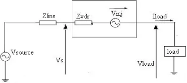
Above figure shows the equivalent circuit of the DVR, when the source voltage is drop or increase, the DVR injects a series voltage through the injection transformer so that the desired load voltage magnitude can be maintained.
The series injected voltage magnitude can be maintained. The series injected voltage of the DVR can be written as
= + (1)
Where; is the desired load voltage magnitude
is the source voltage during sags/swells condition .
The load current is given by,
(2)
III. PROPOSED METHOD
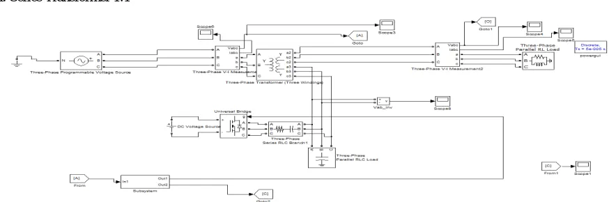
Figure 3 shows the configuration of the proposed DVR design using MATLAB/SIMULINK, where the outputs of a three-phase half-bridge inverter are connected to the utility supply via wye-open connected series transformer. Once a voltage disturbances occurs, with the aid of dqo transformation based control scheme, the inverter output can be steered in phase with the incoming ac source while the load is maintained constant. As for the filtering scheme of the proposed method, output of inverter is installed with capacitors and inductors.
IV. DESIGN OF DVR
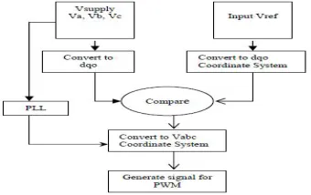
Control unit is the heart of DVR. The basic function of a controller in a DVR are the detection of voltage sag/swell events in the system, generation of trigger pulses to the sinusoidal PWM based DC-AC inverter, computation of the correcting voltage, correction of any anomalies in the series voltage injection and termination of the trigger pulses when the event has passed. The controller may also be used to shift the DC-AC inverter into rectifier mode to charge the capacitors in the DC energy link in the absence of voltage sags/swells. The dqo transformation or park’s transformation [6-7] is used to control of DVR. The dqo method gives the sag depth and phase shift information with start and end times. The quantities are expressed as the instantaneous space vectors. Firstly convert the voltage from a-b-c reference frame to d-q-o reference. Zero sequence component is ignored.The control scheme for the proposed system is based on the comparison of actual voltage and desired voltage. There are two, three phase programmable voltage source in the proposed system configuration, one is reference voltage and another one is measured terminal voltage. Control scheme will follow these voltage sources continuously. Comparison of reference voltage source and measured terminal voltage will generate the error signal. The error signal is used as a modulation signal that allows to generate a commutation pattern for the power switches (MOSFET’s) constituting the voltage source converter. The commutation pattern is generated by means of the sinusoidal pulse width modulation technique (SPWM); voltages are controlled through the modulation.
ISSN (Print) : 2320 – 3765 ISSN (Online): 2278 – 8875
I
nternational
J
ournal of
A
dvanced
R
esearch in
E
lectrical,
E
lectronics and
I
nstrumentation
E
ngineering
(An ISO 3297: 2007 Certified Organization)
Vol. 3, Issue 7, July 2014
=
Above equation defines the transformation from three phase system abc to dqo stationary frame. In this transformation, phase A is aligned to the d-axis that is in quadrature with the q-axis. The theta ( ) is defined by the angle between phase A to the d-axis.The angular velocity ω and displacement are related by
= ⨜ω dt
The control system employs abc to dqo transformation to dqo voltages. During normal condition and symmetrical condition, the voltage will be constant and d-voltage is unity in p.u. and q-voltage is zero in p.u. but during the abnormal conditions it varies. After comparison d-voltage and q-voltage with the desired voltage, error d and error q is generated. These error component is converted into abc component using dqo to abc transformation. Proposed control technique block is shown in the figure below:
Figure 5: control circuit of DVR
V. SIMULATION MODEL
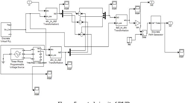
Proposed system configuration is prepared in Simulink. Since DVR is series connecting device so it will connect in series in the distribution system. Here programmable voltage source is used as a source voltage. L.V. side of injection transformer is connected to voltage sourced converter. Error voltage generated through comparison of reference voltage with actual measured voltage of system and hence switching pulses of voltage source converter will generate by discrete PWM generator. VSC used in this paper is MOSFET based power electronic device. Voltage source converter will supply ac voltage through injection transformer.
VI. SIMULATION RESULTS AND DISCUSSION
V.1 Voltage Sags
ISSN (Print) : 2320 – 3765 ISSN (Online): 2278 – 8875
I
nternational
J
ournal of
A
dvanced
R
esearch in
E
lectrical,
E
lectronics and
I
nstrumentation
E
ngineering
(An ISO 3297: 2007 Certified Organization)
Vol. 3, Issue 7, July 2014
transients. The effectiveness of the DVR under unbalanced conditions with 40% single phase voltage sag on a utility grid is shown in the figure. DVR will keep the load voltages constant at 1 p.u.
(a)
(b)
(c)
Figure 6: three phase voltage sag (a)source voltage (b)injected voltage (c)load voltage
(a)
ISSN (Print) : 2320 – 3765 ISSN (Online): 2278 – 8875
I
nternational
J
ournal of
A
dvanced
R
esearch in
E
lectrical,
E
lectronics and
I
nstrumentation
E
ngineering
(An ISO 3297: 2007 Certified Organization)
Vol. 3, Issue 7, July 2014
(c)
Figure 7: single phase voltage sag (a)source voltage (b)injected voltage (c)load voltage
V.2 Voltage swells
The second simulation shows the DVR performance during a voltage swell condition. The simulation started with 40% voltage swell for duration 0.1 second. DVR operate very quickly and inject appropriate negative magnitude voltage to compensate supply voltage.
(a)
(b)
(c)
ISSN (Print) : 2320 – 3765 ISSN (Online): 2278 – 8875
I
nternational
J
ournal of
A
dvanced
R
esearch in
E
lectrical,
E
lectronics and
I
nstrumentation
E
ngineering
(An ISO 3297: 2007 Certified Organization)
Vol. 3, Issue 7, July 2014
(a)
(b)
(c)
Figure 9: single phase voltage swell (a)source voltage(b)injected voltage(c)load voltage
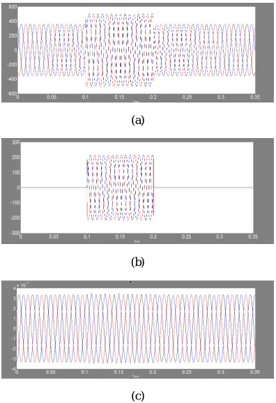
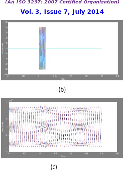
V.3 when the supply voltage contains harmonics:
DVR is also simulated by considering the harmonics present in the normal supply voltage. Supply voltage consists higher order harmonics for duration .1 s to .12 s and it will simulate for total duration 0.02 s. DVR will inject appropriate voltage to compensate for the harmonics and keeps the load voltage at its fundamental.
ISSN (Print) : 2320 – 3765 ISSN (Online): 2278 – 8875
I
nternational
J
ournal of
A
dvanced
R
esearch in
E
lectrical,
E
lectronics and
I
nstrumentation
E
ngineering
(An ISO 3297: 2007 Certified Organization)
Vol. 3, Issue 7, July 2014
(b)
(c)
Figure 10: supply voltage containing harmonics(a)source voltage(b)injected voltage(c)load voltage
Figure 11: FFT analysis of source voltage
ISSN (Print) : 2320 – 3765 ISSN (Online): 2278 – 8875
I
nternational
J
ournal of
A
dvanced
R
esearch in
E
lectrical,
E
lectronics and
I
nstrumentation
E
ngineering
(An ISO 3297: 2007 Certified Organization)
Vol. 3, Issue 7, July 2014
DVR reduces the THD of 33% at source voltage to 1.61% at load voltage, showing the proper operation.
VI. CONCLUSION
The modelling and simulation of a DVR using MATLAB/SIMULINK has been presented. A control system based on dqo technique which is a scaled error between source side of the DVR and its reference for sag/swell correction has been presented. The simulation shows that the DVR performance is satisfactory in mitigating voltage sags/swells . DVR can also compensate for harmonic voltage. Its proper operation shows that DVR reduces the THD from faulted voltage to corrected constant load voltage. DVR handles both balanced and unbalanced situations to keep the load voltage balanced and constant at the nominal value.
VII. APPENDIX: SYSTEM DATA
1. Supply Voltage =440 V
2. Line frequency = 50 HZ
3. DVR DC voltage = 440 V
4. Series Transformer 1:1
Figure 3: proposed system configuration
REFERENCES
[1] N.G. Hingorani, “Introducing Custom Power in IEEE Spectrum,” 32p, pp. 4l-48, 1995. [2] IEEE Std. 1159 – 1995, “Recommended Practice for Monitoring Electric Power Quality”.
[3] P. Boonchiam and N. Mithulananthan, “Understanding of Dynamic Voltage Restorers through MATLAB Simulation,” Thammasat Int. J. Sc. Tech., Vol. 11, No. 3, July-Sept 2006.
[4] J. G. Nielsen, M. Newman, H. Nielsen,and F. Blaabjerg, “Control and testing of a dynamic voltage restorer (DVR) at medium voltage level,” IEEE Trans.Power Electron., vol. 19, no. 3,p.806,May 2004.
[5] A. Ghosh and G. Ledwich, “Power Quality Enhancement Using Custom Power Devices,”Kluwer Academic Publishers, 2002.
[6] S. Chen, G. Joos, L. Lopes, and W. Guo, "A nonlinear control method of dynamic voltage restorers," in 2002 IEEE 33rd Annual Power Electronics Specialists Conference, 2002, pp. 88- 93.