Page | 168
Heart Rate Monitoring of Patient Using GSM
Thatikonda Mounish
B.Tech Department of Electronics and Communication Engineering Sri Venkateswara College of Engineering and Technology
(Affiliated to JNTUA, Ananthapur, Approved by AICTE, New Delhi, Accredited by National Board of Accreditation (NBA). New Delhi, NAAC., Bangalore,
An ISO 9001:2000 Certified Institution) RVS NAGAR, CHITTOOR -517127.
ABSTRACT
In this fast pace world it is difficult for people to be constantly available for their near ones who might need them while they are suffering from any diseases or physical disorder. This is so for especially cardiac patients who need to be monitored continuously by their doctor to verify their heart rate. This would be difficult for the doctors to be present besides their patient all time. Hence to lessen excessive burden of continuously monitoring patient’s heart rate from doctor’s head, we are proposing a patient heart rate monitoring system using GSM. The system includes a data acquisition & processing module which receives physiological data from the patient and GSM module to transmit the acquired data to the doctor’s mobile. This measured data could be an important indicator for prognosis and diagnosis, and also could be shared with their physician anytime to seek medical advice when needed.
The goal of this project is to present our design of this compact sized and user friendly accessory that can be accounted in clinical care and practice
.
INTRODUCTION
1.1 Objective:
The main objective of this project is to provide a means of a portable heart rate monitor for patients suffering from cardio vascular diseases like „tachycardia‟ and „arrhythmia‟ and also share with their
physician through an SMS any time when needed.
1.2 Existing System:
Cell Phones commonly used for communication purposes can also be used as a means for monitoring the health condition. Recent studies have shown that using tele-monitoring devices along with patient communication has a significant impact on efficiency of care and impact on life. Although this is a significant breakthrough it restricts the patient from leaving his/her home without being tele-monitored to keep track of his/her medical condition. This can be overcome by using a simple hardware system comprising the necessary sensors and GSM circuit for transmitting the data measured to the doctor through an SMS.
1.3 Proposed System:
The proposed system consists of a simple wearable heart rate sensor of clip type and a GSM board both of which are connected to an LPC2148 ARM board. This system provides a portable heart rate monitoring device especially for patients suffering cardio vascular diseases and helps them continuously keep track of their heart rate and share the data with their physician through an SMS any time for medical attention if needed.
Page | 169
filtering and amplifying. This measured data is sent to the controller which calculates the heart rate in BPM and is sent as an SMS to the doctor through the GSM module attached to it.
2.CIRCUIT DIAGRAM AND
HARDWARE
DESCRIPTION
2.1
BLOCK
DIAGRAM
DESCRIPTION:
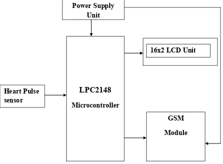
The block diagram of the circuit consists of generally four main components: 2.1.1. LPC2148 Microcontroller
2.1.2. Heart Pulse Sensor 2.1.3. LCD Unit board 2.1.4. GSM Modem
The DC Power supply unit, which drives the entire circuit, is connected to the ARM board as well as to the GSM modem. The heart pulse sensor is connected to one of the port pins of the microcontroller.
1)The LPC2148 Microcontroller forms the heart of the circuit and is used for processing the data supplied form the
pulse sensor for displaying it on an LCD and also for transmitting the data to the GSM modem.
2) The Heart Pulse sensor is simple circuit which works on the principle of Photoplethysmography that using modulation of light as a means to calculate the heart rate. The circuit consists of an optical transceiver that consists of a light source and a receiver. It also consists of an amplifier circuit for amplifying the electric pulse signals received from the optical transceiver. The output of the circuit is of TTL logic which can be directly given to the Microcontroller.
3) The LCD board is a simple 2x16 display unit used for displaying the heart rate measured from the sensor unit, with the help of the Microcontroller to which it is connected.
Page | 170
2.2 BLOCK DIAGRAM:
Fig 2.1: Block Diagram
2.2.1 WORKING PROCEDURE:
First the circuit is switched ON and the ARM Board is reset, to show zero reading on the display. Then the finger tip of the person is clipped with the heart pulse sensor. This circuit measures the pulse impulses of the person for 30sec, and is sent to the Microcontroller which counts the no of pulses received with the help of
an inbuilt timmer and multiplies the counted value by 2 as per the Program written into the circuit and displays the value on the LCD in beats per minute. This value is then sent automatically to the GSM circuit containing a SIM card for communication and sends the value received as an SMS to doctor‟s number specified as per the program.
LPC2148
Microcontroller
Heart Pulse
sensor
GSM
Module
16x2 LCD Unit
Power Supply
Page | 171
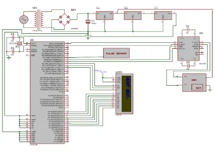
2.3 SCHEMATIC DIAGRAM:
Fig 2.2: Schematic Diagra
3.ARM7
MICROCONTROLLER
3.1 INTRODUCTION:
This technology was introduced by a British company called “ARM Holdings” in 1985. The LPC2141/2/4/6/8 microcontrollers are based on a 32/16 bit ARM7TDMI-S CPU withreal-time emulation and embedded trace support, that combines the microcontroller withembedded high speed flash memory ranging from 32kB to 512kB. A 128-bit widememory interface and unique accelerator architecture enable 32-bit code execution atthe maximum clock rate. For critical code size applications, thealternative16-bit Thumbmode reduces code by more than 30 % with minimal performance penalty.Due to their tiny size and low power consumption, LPC2141/2/4/6/8 are ideal forapplications where miniaturization is a key requirement, such as access control andpoint-of-sale.
A blend of serial communications interfaces ranging from a USB 2.0 FullSpeed device, multiple UARTs, SPI, SSP to I2Cs, and on-chip SRAM of 8kB up to 40kB, make these devices very well suited for communication gateways and protocolconverters, soft modems, voice recognition and low end imaging, providing both largebuffer size and high processing power. Various 32-bit timers, single or dual 10-bit ADC(s),10-bit DAC, PWM channels and 45 fast GPIO lines with up to nine edge or level sensitiveexternal interrupt pins make these microcontrollers particularly suitable for industrialcontrol and medical systems.
Page | 172
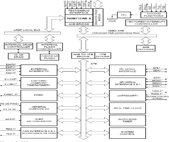
3.1.1 ARM7 BLOCK DIAGRAM:
Fig 3.1: Block Diagram ARM7 Microcontroller
3.1.2 LPC2148 PIN DIAGRAM & DESCRIPTION:
Page | 173
I/O PORT PINS:
It is a 64-pin IC and it consistsof 48 Bidirectional I/O port pins.
48 I/O ports starting from P0.0 to
P0.31, P1.16 to P1.31.
In this 48 pins 3 pins P0.24, P0.26,
P0.27 are reserved.
Each port can have 4 functionalities but only one at a time.
MEMORY ARCHITECTURE:
3.1.4 On chip flash Memory System
The LPC2141/2/4/6/8 incorporates a 32kB, 64kB, 128kB, 256kB, and 512kB Flashmemory system, respectively. This memory may be used for both code and data storage.Programming of the Flash memory may be accomplished in several ways: over the serialbuilt-in JTAG interface, using In System Programming (ISP) and UART0, or by means of Application Programming (IAP) capabilities. The application program, using the IAPfunctions, may also erase and/or program the Flash while the application is running,allowing a great degree of flexibility for data storage field firmware upgrades, etc. Whenthe LPC2141/2/4/6/8 on-chip boot loader is used, 32kB, 64kB, 128kB, 256kB, and 500kB of Flash memory are available for user code.The LPC2141/2/4/6/8 Flash memory provides minimum of 100,000 erase/write cycles and20 years of data-retention.
3.1.4 On-chip Static RAM (SRAM): On-chip Static RAM (SRAM) may be used for code and/or data storage. The on-chipSRAM may be accessed as 8-bits, 16-bits, and 32-bits. The LPC2141/2/4/6/8 provides8/16/32kB of static RAM, respectively.
The LPC2141/2/4/6/8 SRAM is designed to be accessed as a byte-addressed memory.Word and half word accesses to the memory ignore the alignment of the address
andaccess the naturally-aligned value that is addressed (so a memory access ignoresaddress bits 0 and 1 for word accesses, and ignores bit 0 for half word accesses).
Therefore valid reads and writes require data accessed as half words to originate fromaddresses with address line 0 being 0 (addresses ending with 0, 2, 4, 6, 8, A, C, and E in hexadecimal notation) and data accessed as words to originate from addresses withaddress lines 0 and 1 being 0 (addresses ending with 0, 4, 8, and C in hexadecimalnotation). This rule applies to both off and on-chip memory usage.
The SRAM controller incorporates a write-back buffer in order to prevent CPU stallsduring back-to-back writes. The write-back buffer always holds the last data sent bysoftware to the SRAM. This data is only written to the SRAM when another write isrequested by software (the data is only written to the SRAM when software does anotherwrite). If a chip reset occurs, actual SRAM contents will not reflect the most recent writerequest (i.e. after a "warm" chip reset, the SRAM does not reflect the last write operation).Any software that checks SRAM contents after reset must take this into account. Twoidentical writes to a location guarantee that the data will be present after a Reset.Alternatively, a dummy write operation before entering idle or power-down mode willsimilarly guarantee that the last data written will be present in SRAM after a subsequentReset.
3.1.5 Memory remapping:
Page | 174
the interrupt vectors remain in fixed locations.
The portion of memory that is re-mapped to allow interrupt processing in different modesincludes the interrupt vector area (32 bytes) and an additional 32 bytes, for a total
of64 bytes. The re-mapped code locations overlay addresses 0x0000 0000 through 0x0000003F. A typical user program in the Flash memory can place the entire FIQ
handler at address 0x0000 001C without any need to consider memory boundaries. Thevector contained in the SRAM, external memory, and Boot Block must contain branches tothe actual interrupt handlers, or to other instructions that accomplish the branch to theinterrupt handlers.
There are three reasons this configuration was chosen:
1. To give the FIQ handler in the Flash memory the advantage of not having to take a
Memory boundary caused by the remapping into account.
2. Minimize the need to for the SRAM and Boot Block vectors to deal with arbitrary boundaries in the middle of code space. 3. To provide space to store constants for jumping beyond the range of single word branch instructions.
Re-mapped memory areas, including the Boot Block and interrupt vectors, continue toappear in their original location in addition to the re-mapped address.
4.SOFTWARES USED
In our project we mainly use three softwares:
1. Keil software 2. Flash Magic 3. Proload
4.1 KEIL software:
Keil compiler is software used where the machine
language code is written and compiled.
After compilation, the machine source code is converted into hex code which is to be dumped into the microcontroller for further processing.
Keil compiler also supports C language code.
Keil can be used to create source files,automatically compile,link and convert using option set.
4.2 FLASH MAGIC:
NXP features include the following:
ErasingtheFlashmemory(individualblockso rthewholedevice).
ProgrammingtheFlashmemory
ModifyingtheBootVectorandStatusByte ReadingFlashmemory
PerformingablankcheckonasectionofFlash memory
Readingthesignaturebytes
Readingandwritingthesecuritybits
Directloadofanewbaudrate(highspeedcomm unications)
SendingcommandstoplacedeviceinBootload ermode
FlashMagicprovidesaclearandsimpleuserint erfacetothesefeaturesandmoreas
describedinthefollowingsections.
UnderWindows,onlyone
applicationmayaccesstheCOMPortatany time,
Page | 175
NotethatinthismanualthirdpartyCompile rsarelistedalphabetically.Nopreferences are indicatedorimplied.
4.3 PROLOAD:
Proload is software which accepts only hex files. Once the machine code is converted into hex code, that hex code has to be dumped into the microcontroller placed in the programmer kit and this is done by the Proload. Programmer kit contains a microcontroller on it other than the one which is to be programmed. This microcontroller has a program in it written in such a way that it accepts the hex file from the keil compiler and dumps this hex file into the microcontroller which is to be programmed. As this programmer kit requires power supply to be operated, this power supply is given from the power supply circuit designed above. It should be noted that this programmer kit contains a power supply section in the board itself but in order to switch on that power supply, a source is required. Thus this is accomplished from the power supply board with an output of 12volts or from an adapter connected to 230 V AC.
1. Install the Proload Software in the PC.
2. Now connect the Programmer kit to the PC (CPU) through serial cable.Power up the programmer kit from the ac supply through adapter. 3. Now place the microcontroller in
the GIF socket provided in the programmer kit
4. After this process is completed, remove the microcontroller from the programmer kit and place it in your system board. Now the system board behaves according to the program written in the microcontroller.
5.APPLICATIONS:
1. This circuit can normally be used for patients for monitoring their hear rate at home.
2. This circuit can also be used in hospitals for monitoring purposes. 3. This circuit can also be used for the
training athletes during workouts for exercising below their maximum heart rates specified by their doctors.
4. The heart rate monitor can keep runners in their peak target zones during intense training and at aerobic base during easier sessions. 5. This system can also be used for the
weight-loss participants by making the circuit to display the calories burnt during workout and share the data with their dietician.
6.LIMITATIONS:
1. The photoplethysmography technique is slightly prone to interference of ordinary light. 2. The circuit may be sensitive to
temperature variations and the output may vary between 20% of the true value.
3. The no of SMS processed by the GSM module is very small 6 to 10 messages per minute.
7.CONCLUSION:
Thus in this project the heart rate of the patient is calculated using the heart pulse sensor based on the Photopletysmography technique. This pulse rate measured is displayed in the form of beats per minute (BPM) and displayed on the LCD for the patients reference. This measured heart rate is also sent as an SMS to the doctor for any medical attention needed.
8.FUTURE SCOPE:
Page | 176
levels in patients‟ blood and also the breathing rates of the patient. This system can be further extended to a level of a complete house hold health monitoring system, reducing the need for further testing at the hospitals and saving time.
9. REFERENCES
[1.] M.Engin, E.Caglav, E.Z.Engin,
“Real-time ECG Signal
transmission via telephone network”, Measurement, vol. 37,pp.167-171, 2005
[2.] B.H.Yang and S.Rhee, “Development of the ring sensor for health-care automation”, Robotics and Autonomous Systems, vol.30, pp. 273-281, 2000.
[3.] M.Engin, A.Demirel, E.Z.Engin,
and N.Fedakr, “Recent
development and trends in biomedical engineering”, Measurement,volume.37,pp.173-188,2005
[4.] J.G.Webster, Medical instrumentation, john wiely and sons In., New York,1988
[5.] M.I.Owis, A.H.Abou-Zied ,A.M.Youssef, and Y.M.Kadah, “Study of features based on non linear modeling in ECG arrhythmia detection and classification “, IEEE Trans. on biomedical Eng., vol.49,pp.733-736,2002
[6.] F.Ahmad, M.I.Eibrahimy, M.A.M.Ali, and E.Jahedi, “A
portable term fetal heart rate monitoring”
,Microprocessor and
Microsystem,vol.26,pp.323-330,2002
[7.] M.I.Ibrahimy ,F.Ahmad, M.A.M.Ali,and E.Zahedi, ”Real time signal processing for fetal heart rate monitoring”, IEEE trans. On Biomedical Eng., vol.50, pp.258-262, 2003.
[8.] J.J.Carr and J.M.Brown, introduction to biomedical
equipment technology, Prentice hall new jersey,2001
[9.] Jayasree et al., -Design and Development of simple Hardware Setup for Sensing Blood Volume Pulse and a PIC Microcontroller Based Heart Rate Meter||, intl. conf. on Biomedical and Pharmaceutical Engineering (ICBPE), Research Publishing Services, ISBN:81-90426-1-4,pp. 256-258, 2006. [10.] K.D. Taylor, and M.
Mandelberg, -Precision Digital Instrument for Calculation of Heart Rate and R-R Interval||, IEEE Transactions on Biomedical Engineering,pp.255-257,1975. [11.] Rotariu rt al. –Telemedicine
System for Remote Blood Pressure and Heart Rate Monitoring||, Proceeding of the 3rd International Conference on E- Health and Bioengineering,2011.
[12.] Edwards S., -Heart Rate Monitor Book||, Leisure systems International, 1993
[13.] Hashem et al., -Design and Development of a Heart Rate Measuring Device using fingertip||, IEEE International Conference on Computer and Communication Engineering Technology (ICCCE), ISBN:978-1-4244-6235-3,2010. [14.] Kang et al., -A wrist –worn
integrated health monitoring instrument with tele-reporting device for telemedicine and telecare|| IEEE Transactions on Instrumentation and Measurement, Issue 5, vol.55,pp.1655-661,2006. [15.] Yonezawa et al., -A
Precision Digital Instantaneous Heart Rate Meter with a wide Range||, IEEE Transactions on Biomedical Engineering, Vol. BME-30, No.9,pp.621-615,1983. [16.] Ibrahim D and Buruncuk K.
Page | 177
Link:www.emo.org.tr/ekler/a568a2 aa8c19a31_ek.pdf.
[17.] Edwards S.,-Heart rate Monitor Book||, Leisure systems International,1993.
[18.] Chen M, -The Influence of Resting Heart Rate to Cardio Vascular Disease Prognosis||, Hainan Medical Journal, 2007. [19.] H. Miwa and K. Sakai ,
-Development of Heart Rate and Respiration Rate Measurement
System Using Body-Sound||, Proceedings of the 9th International Conference on Information Technology and Applications in Biomedicine (ITAB),ISBN: 978-1-4244-5379-5,pp. 1-4,2009.