IJEDR1603087
International Journal of Engineering Development and Research (www.ijedr.org)530
Analysis of Temperature Effect on MOSFET
Parameter using MATLAB
1Jitty Jose,
2Keerthi K Nair,
3Ajith Ravindran
1P.G Scholar, 2P.G Scholar, 3Assistant Professor 1Electronics and communication Engineering, Saintgits College of Engineering, Kottayam India
________________________________________________________________________________________________________
Abstract— It is well known that the device performance and characteristics are influence by change in operating
temperature. Proper description of temperature effects in a device is essential for a circuit level MOSFET model to predict circuit behavior over a wide range of temperature. To perform high temperature application, proper understanding of temperature dependent parameter in MOSFET is critical. In a MOSFET model , there are many temperature dependent parameters such as bandgap, carrier mobility, threshold voltage, subthreshold leakage current, drain to source ON resistance, contact region resistance, saturation velocity etc. All of this parameters need to be modelled correctly. This paper deals with analysis of temperature effect on some of the MOSFET parameters like bandgap, carrier mobility, saturation velocity and contact region resistance. The analysis of all the effect are done by using mathematical simulation. The overall impact of these parameters on the characteristics of the MOSFET have been analyzed
IndexTerms—MOSFET, Temperature dependence parameter, mathematical modelling, device simulation
________________________________________________________________________________________________________
I.INTRODUCTION
Today, one of the critical issue faced by the semiconductor industry is thermal reliability. So this indicate that temperature plays a critical role in performance and efficiency of the device. When an IC is operational, heat dissipation will occur within the device. This is called self-heating of the device and this self-heating of the ICs is burn in environment leads to a series of issue that affects the reliability of the device. It leads to large current, greater junction temperature and can result in thermal runaway and even ultimately rendering the device useless.
A high end device should be productive efficiently and exhibits good performance for a high range of temperature. In order to optimize the performance of the device, the parameter that comes in the case of MOSFET scenario are bandgap optimization , subthreshold leakage issue, carrier mobility and saturation velocity , the resistance at contact and interface like source and drain. This work is focused on analyzing the variation of each of these parameters with the variation in temperature. This effect of temperature on the device parameters, only if analyzed and modelled, its effect on device performance can be known and hence the better performing highly reliable device can be developed.
II.BANDGAP
The temperature is a pre-eminent parameter of electronics system that affect the characteristics of the device in a number of fundamental ways. The most elementary property is the energy bandgap Eg, which is affected by the temperature according to the Varshni’s equation. The study of the temperature effect on bandgap structure is very important because it is directly related to device electrical properties. The bandgap can be defined as the energy difference between top and bottom of conduction band and valence band in insulator and semiconductor. It is expressed in electron votls (eV). The conductivity of semiconductor is immensely depends on the bandgap.
The bandgap is indirectly related to the temperature that is bandgap of semiconductor decrease with increase in temperature. When temperature is increase, the vibration of atoms are increase, which leads to higher interatomic spacing. The interaction between freely moving carriers that is electron and holes and lattice phonons will also affect the bandgap to a smaller extent. The relation between bandgap energy and temperature can be described by Varshni’s empirical expression [1]
𝐸𝑔 (𝑇) = 𝐸𝑔(0) − 𝛼𝐸𝑇2
𝑇+𝛽𝐸 (1) Where,
𝐸𝑔(0)=Band gap energy at absolute zero kelvin
𝛼𝐸, 𝛽𝐸= Material-specific constant
IJEDR1603087
International Journal of Engineering Development and Research (www.ijedr.org)531
Figure 1. The temperature dependence of the band gap of Si, Ge, GaAs.
The characteristic shows the parabolic decrease in bandgap of the semiconductor as the temperature is increased. On checking the bandgap at room temperature (273 K) it is clear that the experimental value matches the theoretical value and the band gap of Si is 1.14 eV. On increasing the temperature, the atomic spacing increases due to the thermal expansion of the energy states which is in turn due to the increased lattice vibrations and this results in lowering of the band gap. Checking the band gap at 300 K we can find a considerable reduction in bandgap that is, band gap here is reduced to 1.125 eV from 1.14 eV at room temperature .If the bandgap is observed at lower temperature, the lattice vibrations will be lower and hence the band gap at 0K is 1.17 eV which is much higher than the bandgap at room temperature. At 600 k the bandgap is reduced to 1.032. At the 300K, bandgap of GaAs and Ge are 1.43 and 0.66. The bandgap of these materials are also decrease with increase temperature.
III.CARRIERMOBILITY
Carrier mobility can be considered as one of the crucial temperature dependent MOSFET parameter. The carriers are commonly refers to electrons and holes. In semiconductor physics, the electron mobility refers to how rapidly an electron will move through a metal or semiconductor, when pulled by an electric field [3]. In semiconductor, there is a homologous quantity for holes, called hole mobility. The conductivity of a semiconductor is directly proportional to the product of carrier concentration and carrier mobility. Whenever all the things are equal, higher mobility leads to better device performance.
Factors depends up on the mobility of carriers in the semiconductors are donor and accepter concentration, defect concentration, and also the temperature. From the Bose-Einstein distribution, it reveals that phonon scattering is strongly a temperature dependent parameter. Since the density of phonon increases with temperature, which causes increase in scattering. [4]. Thus lattice scattering lowers the carrier mobility more and more at higher temperature. The carrier mobility is the vital parameter for the numerical simulation of the electrical characteristics on semiconductor devices. In order to capture the dependence of mobility on temperature, doping, and the electric field, different mathematical models were developed. The carrier mobility are given by the equation [5]
𝜇(𝑇) = 𝜇(𝑇𝑟)( 𝑇 𝑇𝑟)
𝑘𝜇 (2)
Where,
T = Absolute temperature, Tr = Room temperature
kμ = Fitting parameter with a typical value of about 1.5
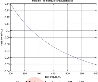
𝜇(𝑇𝑟) =ref. temp (300K) = 0.14 m2/v.s
The analytical modelling of carrier mobility is shown in figure 2 and it revels the inverse relationship between temperature and carrier mobility.
0 100 200 300 400 500 600
0.4 0.6 0.8 1 1.2 1.4 1.6 1.8
temprature,/K
B
a
n
d
g
a
p
,/
e
V
Bandgap - temprature characteristics
IJEDR1603087
International Journal of Engineering Development and Research (www.ijedr.org)532
Figure 2. The temperature dependence of the mobility.
From the figure 2 the value of carrier velocity for Si at room temperature, 300K is 0.14 m2/V.s which matches the theoretical value [6]. A 100o C, in temperature may decrease the mobility by as much as 40%. The result is a proportional decrease in drain current, for a fixed applied voltage.so current consumption of the entire circuit may decrease considerably at high temperature. The maximum speed of operation thus decreases in proportion. The change in threshold voltage and mobility affects the drain current, the Trans conductance, and the drain to source ON resistance of MOSFET.
IV.CONTACT REGION RESISTANCE
The rapidly growing CMOS technologies, lack of proper understanding of the physical and analytical mechanisms of parasitic resistance will leads to the minimization of better performance of device used in various VLSI circuit applications. As CMOS technology push forward, the junction depth of the source/drain and size of other related device features are being ambitiously reduced so the effect of source/drain resistance on the device performance become increasingly significant. As the CMOS technology advances, the parasitic drain/source resistance component does not scale with device dimensions and thereby give a substantial fractions of the total resistance, resulting in appreciable degradation of current driving capability [7-10] Additionally for the analysis of schottky contact MOSFET, exact modelling of the silicide/ Si contact resistance is necessary[11].
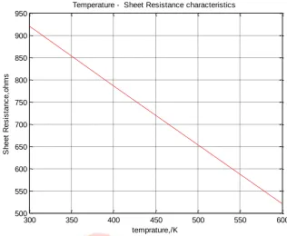
Contact resistance component’s parasitic resistance is not adaptable as it simply increases with decrease in contact size equivalent with device scaling [12]. Temperature effects involved in the contact resistance become more momentous in the deep submicron device regime, especially under greater current stress conditions. The change of resistance can be calculated by the equation [13]
𝑅𝐷𝑆, = 920 −4
3(𝑇 − 300) (3)
R,
DS= Total drain and source contact region resistance at high temperature.
The parasitic resistance is also known as sheet resistance. The sheet resistance variation with temperature are shown in figure 3. From the graph it is observed that the value of sheet resistance at 600 K becomes almost half of the value at 300 K.Therefore, smaller voltage drop occurs at drain and source contacts, and the channel has more drain to source voltage, which eventually causes the drain current to increase. The resistance values reduces in linear manner. Therefore, a linear approximation has been made in the calculation of the resistances
300 350 400 450 500 550 600
0.04 0.05 0.06 0.07 0.08 0.09 0.1 0.11 0.12 0.13 0.14
temprature,/K
m
o
b
ili
ty
,m
2/v
.s
IJEDR1603087
International Journal of Engineering Development and Research (www.ijedr.org)533
Figure 3. The temperature dependence of sheet Resistance.
V.SATURATION VELOCITY
When strong electric field is applied to a semiconductor device, the carrier velocity increases to the maximum value and then attains the saturation level. The maximum velocity acquired by the carriers is known as the saturation velocity. When short channel device is considered, the saturation velocity is the key parameter to determine the device performance [14]. Today the microprocessor area uses sub-micron scale semiconductor devices. Velocity saturation become an important design specification parameter in sub-micron scale devices.
The velocity saturation will have larger impact on the voltage transfer characteristics of MOSFETs. After the velocity saturation ohms low will no longer followed that is no linear relation between voltage and current. The raise in current become very small nevertheless of the applied voltage [15].
Sub-micron devices are operates at high electric fields and here precise modelling of saturation velocity is very important to tune up the performance of the devices. In high end devices such as the High Electron Mobility Transistors (HEMTs), saturation velocity is directly proportional to the gain [16]. These high end devices operates at high electric fields, and when this high field is applied, the carrier velocity reaches the peak value and no longer increases after that level because they lose energy through lattice interactions. This interactions leads to photon and phonon emissions which leads to increasing the temperature of the device. And this rise in temperature can eventually affect the overall performance of the device.
The relation between velocity saturation and temperature is given by the following equation
𝑉𝑠𝑎𝑡=
𝑉𝑠𝑎𝑡(300𝑘)
(1−𝐴𝑛)+𝐴𝑛(𝑇 300⁄ ) (4) Where,
Vsat(300k)= Saturation velocity at 300K
An=Temperature coefficient for various material systems
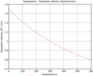
The relation between saturation velocity and temperature are shown in the figure 4. The saturation velocity shows that inverse relation with temperature. From the figure 4 the value of saturation velocity on Si at room temperature is 1*107 cm/s, which matches the theoretical value [17]. At high electric fields, the saturation velocity is the thermal velocity and the typical electric field that saturates the velocity ranges from 10-100kV/cm that can result in a temperature variation from 0-1000K in a semiconductor. Here the saturation velocity for the temperature range from 0 to 600K is plotted and the graph obtained shows the indirect relationship. In addition to the temperature dependence, both the saturation field and saturation velocity of a semiconductor depends strongly on the impurities and lattice defects.
300 350 400 450 500 550 600
500 550 600 650 700 750 800 850 900 950
temprature,/K
S
h
e
e
t
R
e
s
is
ta
n
c
e
,o
h
m
s
IJEDR1603087
International Journal of Engineering Development and Research (www.ijedr.org)534
Figure 4. The temperature dependence of saturation velocity. VI.CONCLUSION
Metal Oxide Semiconductor Field Effect Transistor (MOSFET) device scaling plays an important role in the rapid development of semiconductor industry. Evaluation of temperature dependence of the device characteristics is important for designing scaled down MOS integrated circuit that generally operates over a wide range of temperature It is well known that the change in the operating temperature of a device will influence its characteristics and hence the circuit performance. Accurate description of temperature effects in a device is necessary for a circuit level MOSFET model to predict circuit behaviors over a range of temperature. An IC does not always work under room temperature. Some effects are not prominent in room temperature, have adverse effect in higher temperature ranges.Temperature analysis done in reliability perspective can be used for performance enhancement. Now a days the pre analysis and post analysis of temperature dependent MOSFET parameters are essential for the device used in high temperature applications.
VII.ACKNOWLEDGMENT
Sincerely acknowledge the grace of God and the support of my parents, family, friends and colleagues. I also acknowledge the support of my faculty in this learning process.
REFERENCES
[1] Varshni YP (1967) Temperature dependence of the energy gap in semiconductors. Physica 34:149–154
[2] Gafur, Gulyamov, Sharibaev Nosir Yusupjanovich, and Erkaboev Ulugbek Inoyatillaevich. "The Temperature Dependence of the Density of States in Semiconductors." World Journal of Condensed Matter Physics 2013 (2013). [3] Reggiani, S., et al. "Surface mobility in silicon at large operating temperature." Simulation of Semiconductor Processes
and Devices, 2002. SISPAD 2002. International Conference on. IEEE, 2002.
[4] Dhar, Siddhartha, et al. "Electron mobility model for strained-Si devices."IEEE Transactions on Electron Devices 52.4 (2005): 527-533.
[5] Weste, Neil, David Harris, and Ayan Banerjee. "Cmos vlsi design." A circuits and systems perspective 11 (2005): 739. [6] Darwish, Mohamed N., et al. "An improved electron and hole mobility model for general purpose device
simulation." IEEE Transactions on Electron Devices 44.9 (1997): 1529-1538.
[7] K. K. Ng and W. L. Lynch, “The impact of intrinsic series resistance on MOSFET scaling,” IEEE Trans. Electron Device, Vol. ED-34, No. 3, pp. 503-511, 1987..
[8] P. K. Chatterjee, W. R. Hunter, T. C. Holloway, and Y. T. Lin, “The impact of scaling laws on the choice of n-channel and pchannel for MOS VLSI,” IEEE Electron Device Lett., Vol. EDL-1, pp. 220-223, 1980.
[9] M. Jeng, J. E. Chung, P. Ko, and C. Hu, “The effect of source/drain resistance on deep submicrometer device performance,” IEEE Trans. Electron Devices, vol. 37, No. 11, pp. 2408-2410, 1990.
[10] K. Banerjee, A. Amerasekera, G. Dixit and C. Hu, “Temperature and current effects on small-geometry-contact resistance,” Tech. Dig. IEDM, pp. 115-118, 1997.
0 100 200 300 400 500 600
0.7 0.8 0.9 1 1.1 1.2 1.3 1.4
temprature,/K
S
a
tu
ra
ti
o
n
V
e
lo
c
it
y
,1
0
7 c
m
/s
IJEDR1603087
International Journal of Engineering Development and Research (www.ijedr.org)535
[11] M. Ieong, P. M. Solomon, S. E. Laux, H.-S. P. Wong, and D. Chidambarrao, “Comparison of raised and Schottky source/drainMOSFETs using a novel tunneling contact model,” Tech. Dig. IEDM, pp. 1174-1176, 1999.
[12] Oh, Kwang-Hoon, et al. "Modeling of temperature dependent contact resistance for analysis of ESD reliability." Reliability Physics Symposium Proceedings, 2003. 41st Annual. 2003 IEEE International. IEEE, 2003.
[13] Hasanuzzaman, Md, Syed K. Islam, and Leon M. Tolbert. "Effects of temperature variation (300–600 K) in MOSFET modeling in 6H– silicon carbide." Solid-State Electronics 48.1 (2004): 125-132].
[14] Saad, I., et al. "The dependence of saturation velocity on temperature, inversion charge, and electric field in a nanoscale MOSFET." Int J Nanoelectron Mater 3 (2010): 17-34.
[15] Rais, K., et al. "Study of saturation velocity overshoot in deep submicron silicon MOSFETS from liquid helium up to room temperature." Le Journal de Physique IV 4.C6 (1994): C6-19.
[16] Oxley, C. H., et al. "On the temperature and carrier density dependence of electron saturation velocity in an AlGaN/GaN HEMT." IEEE transactions on electron devices 53.3 (2006): 565-567.