Low hardware Accumulator Based 3-Weight Pattern Generation
for Boundary Scan
Manthri Lavanya
& K.Saifuddin
1
M.Tech ,Assistant Professor, Department of ECE, Anantha Lakshmi Institute of Technology,
Anantapur, Ap, India.
2
M.Tech ,Assistant Professor, Department of ECE , Srinivasa Ramanujan Institute of Technology,
Anantapur, Ap, India.
ABSTRACT:
Weighted pseudorandom built-in self test (BIST) schemes have been utilized in order to drive down the number of vectors to achieve complete fault coverage in BIST applications. Weighted sets comprising three weights, namely 0, 1, and 0.5 have been successfully utilized so far for test pattern generation, since they result in both low testing time and low consumed power. In this paper an accumulator-based 3-weight test pattern generation scheme is presented; the proposed scheme generates set of patterns with weights 0, 0.5, and 1. Since accumulators are commonly found in current VLSI chips, this scheme can be efficiently utilized to drive down the hardware of BIST pattern generation, as well. Comparisons with previously presented schemes indicate that the proposed scheme compares favorably with respect to the required hardware.
Keywords:
Memory BIST, Address Generation, ALU-based implementation.I. INTRODUCTION
Pseudorandom built-in self test (BIST) generators have been widely utilized to test integrated circuits and systems. The arsenal of pseudorandom generators includes, among others, linear feedback shift registers (LFSRs) [1], cellular automata [2], and accumulators driven by a constant value [3]. For circuits with hard-to-detect faults, a large number of random patterns have to be generated before high fault coverage is achieved. Therefore, weighted pseudorandom techniques have been proposed where inputs are biased by changing the probability of a “0” or a “1” on a given input from 0.5 (for pure pseudorandom tests) to some other value [10], [12].
Weighted random pattern generation methods relying on a single weight assignment usually fail to achieve complete fault coverage using a reasonable number of test patterns since, although the weights are computed to be suitable for most faults, some faults may require long test sequences to be detected with these weight the
assignments if they do not match their activation and propagation requirements. Multiple weight assignments have been suggested for the case that
different faults require different biases of the input combinations applied to the circuit, to ensure that a relatively small number of patterns can detect all faults [4]. Approaches to derive weight assignments for given deterministic tests are attractive since they have the potential to allow complete coverage with a significantly smaller number of test patterns [10]. In order to minimize the hardware implementation cost, other schemes based on multiple weight assignments utilized weights 0, 1, and 0.5. This approach boils down to keeping some outputs of the generator steady (to either 0 or 1) and letting the remaining outputs change values (pseudo-) randomly (weight 0.5). This approach, apart from reducing the hardware overhead has beneficial effect on the consumed power, since some of the circuit under test (CUT) inputs (those having weight 0 or 1) remain steady during the specific test session [30]. Pomeranz and Reddy [5] proposed a 3-weight pattern generation scheme relying on weights 0, 1, and 0.5. The choice of weights 0, 1, and 0.5 was done in order to minimize the hardware implementation cost. Wang [2], [8] proposed a 3-weight random pattern generator based on scan chains utilizing weights 0, 1, and 0.5, in a way similar to [5]. Recently, Zhang et al. [9] renovated the interest in the 3-weight pattern generation schemes, proposing an efficient compaction scheme for the 3-weight patterns 0, 1, and 0.5. From the above we can conclude that 3-weight pattern generation based on 3-weights 0, 1, and 0.5 has practical interest since it combines low implementation cost with low test time.
Current VLSI circuits, e.g., data path architectures, or digital signal processing chips commonly contain arithmetic modules [accumulators or arithmetic logic units (ALUs)]. This has fired the idea of arithmetic BIST (ABIST) [6]. The basic idea of ABIST is to utilize accumulators for built-in testing (compression of the CUT responses, or generation of test patterns) and has been shown to result in low hardware overhead and low impact on the circuit normal operating speed [2]–[5]. In [6], Manich et al.
properly selected. However, modules containing hard-to-detect faults still require extra test hardware either by inserting test points into the mission logic or by storing additional deterministic test patterns [4], [12].
In order to overcome this problem, an accumulator-based weighted pattern generation scheme was proposed in [11]. The scheme generates test patterns having one of three weights, namely 0, 1, and 0.5 therefore it can be utilized to drastically reduce the test application time in accumulator-based test pattern generation. However, the scheme proposed in [11] possesses three major drawbacks: 1) it can be utilized only in the case that the adder of the accumulator is a ripple carry adder; 2) it requires redesigning the accumulator; this modification, apart from being costly, requires redesign of the core of the data path, a practice that is generally discouraged in current BIST schemes; and 3) it increases delay, since it affects the normal operating speed of the adder.
In this paper, a novel scheme for accumulator-based 3-weight generation is presented. The proposed scheme copes with the inherent drawbacks of the scheme proposed in [11]. More precisely: 1) it does not impose any requirements about the design of the adder (i.e., it can be implemented using any adder design); 2) it does not require any modification of the adder; and hence, 3) does not affect the operating speed of the adder. Furthermore, the proposed scheme compares favorably to the scheme proposed in [11] and [12] in terms of the required hardware overhead. This paper is organized as follows. In Section II, the idea underlying the accumulator-based 3-weight generation is presented. In Section III, the design methodology to generate the 3-weight patterns utilizing an accumulator is presented. In Section IV, the proposed scheme is compared previously proposed ones. Finally, Section V, concludes this paper.
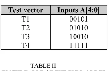
TABLE I
TEST SET FOR THE C17 BENCHMARK
TABLE II
TRUTH TABLE OF THE FULL ADDER
II. ACCUMULATOR-BASED
3-WEIGHT PATTERN GENERATION
We shall illustrate the idea of an accumulator-based 3-weight pattern generation by means of an example. Let us consider the test set for the c17 ISCAS benchmark [12], [3] given in Table I. Starting from this deterministic test set, in order to apply the 3-weight pattern generation scheme, one of the schemes proposed in [5], [8], and [9] can be utilized. According to these schemes, a typical weight assignment procedure would involve separating the test set into two subsets, S1 and S2 as follows: S1 = {T1 , T4} , S2 = {T2 , T3} The weight assignments for these subsets is W(S1) = {-,-,1,-,1} and W(S1) = {-,-,0,1,0} where a “-” denotes a weight assignment of 0.5, a “1“-” indicates that the input is constantly driven by the logic “1” value, and “0”indicates that the input is driven by the logic “0” value. In the first assignment, inputs A[2], and A[0] are constantly driven by “1”, while inputs A[4], A[3], A[1] are pseudo randomly generated (i.e., have weights 0.5). Similarly, in the second weight assignment (subset S2), inputs A[2] and A[0] are constantly driven by “0”, input A[1] is driven by “1” and inputs A[4] and A[3] are pseudo randomly generated. The above reasoning calls for a configuration of the accumulator, where the following conditions are met: 1) an accumulator output can be constantly driven by “1” or “0” and 2) an accumulator cell with its output constantly driven to “1” or “0” allows the carry input of the stage to transfer to its carry output unchanged. This latter condition is required in order to effectively generate pseudorandom patterns in the accumulator outputs whose weight assignment is “-”.
III. DESIGN METHODOLOGY
The implementation of the weighted-pattern generation scheme is based on the full adder truth table, presented in Table II. From Table II we can see that in lines #2, #3, #6, and #7 of the truth table Cout = Cin Therefore, in order to transfer the carry input to the carry output, it is enough to set A[i] =NOT B[i] The proposed scheme is based on
this observation.
presented in Fig. 1, which consists of a Full Adder (FA) cell and a D-type flip-flop with asynchronous set and reset inputs whose output is also driven to one of the full adder inputs. In Fig. 1, we assume, without loss of generality, that the set and reset are active high signals. In the same figure the respective cell of the driving register B[i] is also shown. For this accumulator cell, one out of three configurations can be utilized, as shown in Fig. 2.
Fig. 1. Accumulator cell.
In Fig. 2(a) we present the configuration that drives the CUT inputs When A[i] = 1 is required Set[i] = 1 and Reset [i]= 0 and hence A[i] = 1 and B[i] = 0 Then the output is equal to 1, and Cin is transferred to Cout. In Fig. 2(b) we present the configuration that drives the CUT inputs When A[i] = 0 is required Set[i] = 0 and Reset [i]= 1 and hence A[i] = 0 and B[i] = 1 Then the output is equal to 1, and Cin is transferred to Cout. In Fig. 2(c), we present the configuration that drives the CUT inputs when A[i] = “-“is required Set[i] = 0 and Reset [i]= 0. The D
input of the flip-flop of register B is driven by either 1 or 0, depending on the value that will be added to the accumulator inputs in order to generate satisfactorily random patterns to the inputs of the CUT.
In Fig. 3, the general configuration of the proposed scheme is presented. The Logic module provides the Set[n-1:0] and Reset[n-1:0] signals that drive the S and R inputs of the Register A and Register B inputs. Note that the signals that drive the S inputs of the flip-flops of Register A, also drive the R inputs of the flip-flops of Register B and vice versa.
Fig. 2. Configurations of the accumulator cell of Fig. 1. Are represented in the following forms a, b and figure c as follows.
Fig. 3. Proposed scheme
IV. IMPLEMENTATION AND RESULTS
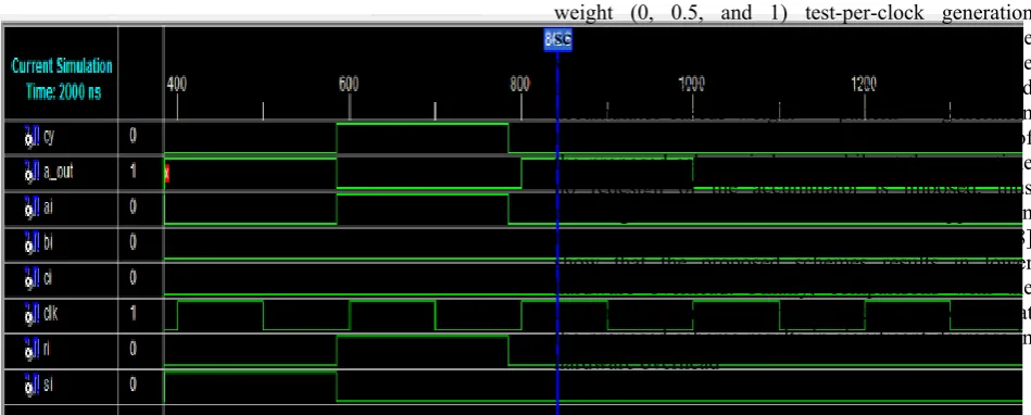
The proposed Low hardware Accumulator Based 3-Weight Pattern Generation for Boundary Scan designed using Verilog hardware description language and structural form of coding. The proposed system simulation results are as follows
Simulation Results
Figure.1 result of accumulator cell
when si = 1 ri = 0 ,and ai = 0 is required then we will get the cy = 0 that will be transferred to the output and a_out = 1.when si = 0 , ri = 1 , and ai = 1 is required then we will get the cy = 1 that will be transferred to the output and a_out = 0 when si = 0 , ri = 0 , and ai = 0 is required then we will get the cy = 0 that will be transferred to the output and a_out = 1
Figure.2 result of 3 weighted pattern generation
The proposed system contains of season counter and lfsr (linear feedback shift register). Which is used to produce internal signals for the different combinations . it produces different combinations of test patterns for given any circuit.
V. CONCLUSION
We have presented an accumulator-based 3-weight (0, 0.5, and 1) test-per-clock generation scheme, which can be utilized to efficiently generate weighted patterns without altering the structure of the adder. Comparisons with a previously proposed accumulator-based3-weight pattern generation technique [11] indicate that the hardware overhead of the proposed scheme is lower while at the same time no redesign of the accumulator is imposed, thus resulting in reduction of 20%–95% in test application time. Comparisons with scan based schemes [5], [8] show that the proposed schemes results in lower hardware overhead. Finally, comparisons with the accumulator- based scheme proposed in [9] reveal that the proposed scheme results in significant decrease in hardware overhead
REFERENCES
[1] P. Bardell, W. McAnney, and J. Savir, Built-In Test For VLSI: Pseudorandom Techniques. New York: Wiley, 1987.
[2] P. Hortensius, R. McLeod, W. Pries, M. Miller, and H. Card, “Cellular automata-based pseudorandom generators for built-in self test,”IEEE Trans. Comput.-Aided Des. Integr. Circuits Syst., vol. 8, no. 8,pp. 842– 859, Aug. 1989.
[4] H. J. Wunderlich, “Multiple distributions for biased random test patterns,” in Proc. IEEE Int. Test Conf., 1988, pp. 236–244.
[5] I. Pomeranz and S. M. Reddy, “3 weight pseudo-random test generation based on a deterministic test set for combinational and sequential circuits,” IEEE Trans. Comput.-Aided Des. Integr. Circuits Syst., vol. 12, no. 7, pp. 1050–1058, Jul. 1993.
[6] K. Radecka, J. Rajski, and J. Tyszer, “Arithmetic built-in self-test for DSP cores,” IEEE Trans. Comput.-Aided Des. Integr. Circuits Syst. vol. 16, no. 11, pp. 1358–1369, Nov. 1997.
[7] J. Rajski and J. Tyszer, Arithmetic Built-In Self Test For Embedded Systems. Upper Saddle River, NJ: Prentice Hall PTR, 1998.
[8] S. Wang, “Low hardware overhead scan based 3-weight 3-weighted random BIST,” in Proc. IEEE Int. Test Conf., 2001, pp. 868–877.
[9] S. Zhang, S. C. Seth, and B. B. Bhattacharya, “Efficient test compaction for pseudo-random testing,” in Proc. 14th Asian Test Symp., 2005, pp.
337–342.[10] J. Savir, “Distributed generation of weighted random patterns,” IEEE Trans. Compute., vol. 48, no. 12, pp. 1364–1368, Dec. 1999.
[10] J. Savir, “Distributed generation of weighted random patterns,” IEEE Trans. Comput., vol. 48, no. 12, pp. 1364–1368, Dec. 1999.
[11] I. Voyiatzis, D. Gizopoulos, and A. Paschalis, “Accumulator-based weighted pattern generation,” presented at the IEEE Int. Line Test Symp., Saint Raphael, French Riviera, France, Jul. 2005.
[12] F. Brglez and H. Fujiwara, “A neutral net list of 10 combinational benchmarks circuits and a target translator in FORTRAN,” presented at the Int. Symp. Circuits Syst., Kyoto, Japan, 1985