ANALYSIS AND DESIGN OF A COMPACT MULTI-LAYER ULTRA WIDE BAND FILTER
D. Packiaraj
Central Research Laboratory Bharat Electronics Limited Bangalore 560013, India
K. J. Vinoy
Department of Electrical Communication Engineering Indian Institute of Science
Bangalore 560012, India
A. T. Kalghatgi
Central Research Laboratory Bharat Electronics Limited Bangalore 560013, India
Abstract—This paper presents analysis and design of a compact ultra wide band (UWB) filter using three parallel folded coupled lines in a defected ground structure in multi-layer structure. Defected ground has been incorporated under the coupled lines of the filter to improve the coupling over a wide bandwidth. The closed form expressions for even and odd mode impedances for the coupled lines with defected ground have been obtained to design a filter of desired bandwidth with the proposed structure. Based on circuit models, an UWB filter for 3.1– 10.6 GHz has been analyzed and the results have been compared using full wave simulations. Analytical results are satisfactorily matching with simulations. Filter exhibits a constant group delay of±0.08 ns in the pass band. Size of the filter is 6.2 mm×3.4 mm×2.8 mm.
of band pass filters with specified pass bands are therefore required to progress in UWB technology. Filters used in UWB systems need to operate over a wide instantaneous bandwidth of 3.1–10.6 GHz with a constant group delay. Extensive work has been carried out to achieve wide band characteristics in the filter performance. A compact wide band filter has been designed based on impedance steps and coupled line sections [1]. Ground plane metallization is removed in these filters to achieve wide band response. Resonators based on slotted ground structures are used in [2] to design compact broad band dual band pass filters. This filter features compact size and frequency selective characteristics with adjustable lower and upper resonance frequencies by changing the size of the resonators. Ultra wide band filter based on quarter wavelength short circuited stubs has also been demonstrated [3]. This has minimal number of vias and improved frequency bandwidth. In [4], wide band and compact band stop filters using one dimensional mushroom like electromagnetic band gap (EBG) are proposed and only fewer EBG cells are used to achieve the desired filter response. The filter is compact with no backward radiation.
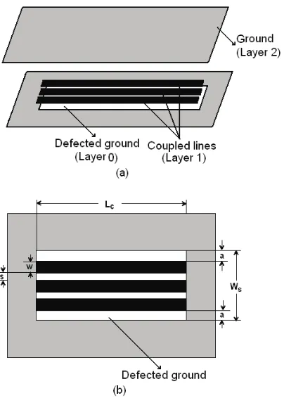
Figure 1. Basic band pass element.
In this paper, a set of three coupled lines shown in Fig. 1(a) having dimensions shown in Fig. 1(b) has been proposed as the basic band pass element to construct a compact UWB filter in multi-layer structure. Ultra wide band response characteristics are achieved using enhanced coupling between the lines in the defected ground. Analysis of this band pass element is explained in Section 2 and closed form expressions for even and odd mode impedances of coupled lines are given for the design of UWB filter. In Section 3, filter is analyzed based on circuit models and analytical results of UWB filter are compared against full wave simulation results for the validation. Section 4 concludes this paper.
2. ANALYSIS OF BAND PASS ELEMENT
Figure 2. Cross section of layers.
coupled line section are extracted from IE3D [11] for the purpose of circuit analysis. Geometrical parameters given in Table 1 are used for the design of UWB filter. Cross section of layers of device is shown in Fig. 2. Layers 0 and 2 are ground conductors. Coupled lines are in layer 1. Layer 0 has defected ground to improve the coupling over wide bandwidth. Coupled line model given in [12] is used to synthesize coupled lines for the desired filter characteristics. Coupled lines are quarter wave long at the center frequency of the filter (6.85 GHz). Coupled line sections are characterized usingABCD parameters, which are given by [12]
A = D= Zoecotθe+Zoocotθo
Z1
(1)
B = j 2
Z2
oe+Zoo2 −2ZoeZoo(cotθecotθo+ cscθecscθo)
Z1
(2)
C = 2j
Z1
(3)
where Z1 = Zoecscθe +Zoocscθo and Zoe and Zoo are even and odd mode impedances of coupled line section respectively. Using differential (positive and negative ports) and common mode (positive ports) excitation features of IE3D [13], even and odd mode impedances of the three parallel coupled line section were extracted and used to
Table 1. Geometrical parameters of band pass element.
Substrate thickness ‘h1’ and ‘h2’ (b=h1+h2)
1000µm, 200µm
Substrate permittivity ‘εr’ 5.99
Conductor thickness 10µm
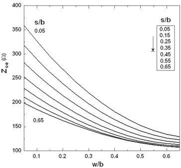
Figure 3. Even mode impedances.
obtain curve-fit expressions as
Zoe = 420−787wb + 528
w
b 2
−522.2s
b1017.56
w
b s b
−505.18
w
b 2s
b
+ 312.7 s
b 2
−397.7
w b s b 2 (4)
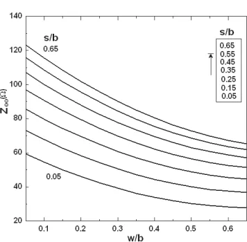
Zoo = 57.18−104.54wb + 79.9
w
b 2
+ 154.9s
b −108.27
w
b s b
+36.75
w
b 2s
b
−62.45 s
b 2
+ 13.82
w b s b 2 (5) for
0.05≤ w
b ≤0.65, 0.05≤ s
b ≤0.65, a= 0.5 mm εr= 5.99 and b= 1.2 mm.
θe is even mode phase velocity and θo is odd mode phase velocity. Equations (4)–(5) are accurate within ±4% tolerance. Zoe and Zoo
for various w/b and s/b are shown in Figs. 3 and 4 respectively for the coupled line section shown in Fig. 1. Coupled line dimensions considered for the design of UWB filter are given in Table 2.
3. DESIGN OF COMPACT MULTILAYER UWB FILTER
Figure 4. Odd mode impedances.
(a) (b)
(c)
Figure 5. Metallization layers of UWB filter. (a) Top layer (layer 2), (b) middle layer (layer 1), (c) bottom layer (layer 0).
Equations (4)–(5). The values of capacitors in the equivalent circuit of the series gap areCa= 0.002 pF andCb = 4 pF. The analytical results
(using MATLAB) are obtained by cascading individual ABCD matrix of UWB filter sections.
Physical parameters defected ground extension ‘a’ and spacing ‘s’ in the structure have influence on bandwidth of the filter. Parametric
Figure 6. Equivalent of UWB filter.
(a)
(b)
Figure 8. Effect of spacing ‘s’ on bandwidth.
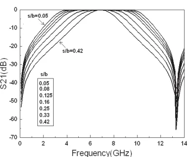
study is carried out to understand the effect of ‘a’ on bandwidth. Fig. 7 shows the results of this parametric study. It shows that bandwidth slightly shrinks as ‘a’ is reduced. Hence appropriate ‘a’ should be chosen while designing the filter with good performance. Spacing ‘s’ in the coupled line sections plays vital role in determining the bandwidth of the filter. Effect of spacing ‘s’ on bandwidth of the filter is shown in Fig. 8. When ‘s’ s reduced, even mode impedance increases, odd mode impedance reduces and tight coupling occurs between the lines and thereby increases the bandwidth. In this paper, ‘a’ and ‘s’ are chosen to be 0.5 mm and 0.1 mm respectively to achieve the required bandwidth of the filter.
Filter is designed using the parameters given in Table 2. Length of each coupled line ‘Lc’ is 4.5 mm and width of lines ‘w’ is 0.1 mm.
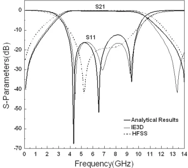
Filter is simulated analytically and using full wave simulators [13, 14]. Results are compared in Fig. 9 and are satisfactorily matching with each other. Pass band of 3.1–10.6 GHz is observed in the filter. The minimum return loss of 15 dB and maximum insertion loss of 0.4 dB
Table 2. Coupled line dimensions.
w 100µm
s 50µm
Lc(λg/4) 4500µm
a 500µm
Figure 9. Characteristics of UWB filter.
Figure 10. Multi-layer UWB filter.
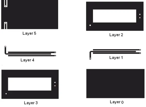
layers and individual layers are shown in Fig. 12. Layers 0 and 5 are ground conductors and Layer 5 has input and output feed lines. Coupled lines are in layers 1 and 4. Defected ground conductors are in Layers 2 and 3. Connecting vias for the coupled lines are made between layers 1 and 4. Ground is isolated in layers 2 and 3 in square shape (0.15 mm×0.15 mm) to isolate the vias as shown in Fig. 12. Substrate with thickness of 0.4 mm (h3) is used between layers 2 and 3 to avoid the cross coupling between the coupled lines.
Figure 12. Layers of multi-layer UWB filter.
compact and size of the filter is 6.2 mm×3.4 mm×2.8 mm.
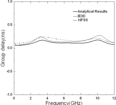
Group delay is one of the parameters that characterizes UWB filter. Group delay is calculated using analytical results and full wave simulations and results are shown in Fig. 14. Group delay is constant over the pass band with±0.08 ns.
Figure 13. S-parameters of multi-layer UWB filter.
coupled line sections were presented to analyze the filter in this paper. Vias were used to connect the folded coupled lines in different layers. This new structure offers wide band response and constant group delay in the pass band. The design of filter was analyzed using circuit models of coupled line and results obtained were validated against the full wave simulations.
REFERENCES
1. Menzel, W., L. Zhu, K. Wu, and F. Bogelsack, “On the design of novel compact broadband planar filters,”IEEE Trans. Microwave Theory Tech., Vol. 51, No. 2, 364–370, Feb. 2003.
2. Wang, X. H. and B. Z. Wang, “Compact broadband dual-band bandpass filters using slotted ground structures,” Progress In Electromagnetics Research, PIER 82, 151–166, 2008.
3. Razalli, M. S., A. Ismail, and M. A. Mahdi, “Novel compact microstrip ultra-wide band filter utilizing short-circuited stubs with less vias,” Progress In Electromagnetics Research, PIER 88, 91–104, 2008.
4. Moghadasi, S. M., A. R. Attari, and M. M. Mirsalehi, “Compact and wideband 1-D mushroom-like EBG filter,” Progress In Electromagnetics Research, PIER 83, 323–333, 2008.
5. Schwab, W., F. Boegelsack, and W. Menzel, “Multilayer suspended stripline and coplanar line filters,” IEEE Trans. Microwave Theory Tech., Vol. 42, No. 7, 1403–1407, Jul. 1994. 6. Hsu, C.-Y., C.-Y. Chen, and C.-H. Huang, “A UWB filter using a
dual-mode ring resonator with spurious pass band suppression,” Microwave Journal, 130–136, Nov. 2005.
7. Ishida, H. and K. Araki, “Design and analysis of UWB band pass filter,”IEEE Topical Conference on Wireless Communication Technology, Honolulu, Oct. 2003.
8. Wong, S. W., L. Z. Zhu, “Quadruple-mode UWB band pass filter with improved out-of-band rejection,” IEEE Microw. Wireless Compon. Lett., Vol. 19, No. 3, 152–154, March 2009.
9. Scrantom, C. Q., “Where we are and where we’re going-II,”IEEE MTT-S IMS Dig., 193–200, 1999.
step impedance quarter-wavelength open stub,” IEEE Trans. Microwave Theory Tech., Vol. 52, No. 2, 617–624, July 2004. 11. Sheen, J. W., “LTCC-MLC duplexer for DCS-1800,”IEEE Trans.
Microwave Theory Tech., Vol. 47, No. 9, 1883–1890, Sep. 1999. 12. Mobbs, C. I. and J. D. Rhodes, “A generalized chebyshev
suspended substrate stripline band pass filter,” IEEE Trans. Microwave Theory Tech., Vol. 31, No. 5, 397–402, May 1983. 13. Zeland Software Inc., “IE3D 11.5”, 2006.