Implementation of Compact LPF Utilizing Defected Structures
and Surface Mount Capacitor for Low Insertion Loss
and Elliptic Characteristics
Alaa M. Abada1, Amr H. Hussein2, *, and Mahmoud A. Attia2
Abstract—Compact size microstrip low-pass filters with sharp cutoff characteristics, narrow passband, low insertion loss, high attenuation in stopband and low cost are highly required in modern wireless communication systems. They are used to suppress the unwanted harmonics and noise caused by Radio Frequency (RF) front ends. In this paper a new design for compact microstrip LPF is proposed. It is based on utilization of Stepped Impedance Resonators (SIR), Defected Microstrip Structure (DMS), Dumbbell-shaped Defected Ground Structure (DB-DGS), and surface mount capacitor. The filter is realized on an F4B-2 substrate with εr = 2.65, thickness h = 0.5 mm and loss tangentδ = 0.0013. The design is carried out using CST-Microwave Studio software. The equivalent circuit of the filter is analyzed and presented using ADS2006A software. The filter exhibits sharp cutoff frequency
fc = 1.7654 GHz, wide stopband from 1.7654 GHz to 7 GHz with |S21| less than −10 dB, insertion loss less than 0.15 dB in passband and reduced size compared to the traditional LPF.
1. INTRODUCTION
There is growing interest in microstrip low-pass filters to equilibrate the stringent requirements of modern wireless communication systems such as compact size, high performances, high selectivity and simplicity using microstrip technology [1]. In recent years, several studies have focused on the design of microstrip low-pass filters and how to enhance their characteristics. Stepped Impedance Hairpin Resonators (SIHRs) for LPF size minimization have been investigated in [2], but this technique suffers from high insertion loss and poor selectivity. A novel microstrip low-pass filter using stepped impedance open stubs is introduced in [3]. Stepped impedance open stubs are used to provide instant transmission zeros at the resonance frequency. However, for smaller transmission zeros, the lengths of the open stubs become very long, which indeed increases the filter size. Defected Ground Structure (DGS) which acts as modification for Photonic Band Gap (PBG) for the design of compact size filters has been introduced in [3] and [4]. Any modification in shapes or dimensions of DGS makes significant changes in the filter characteristics through constituting different currant distribution paths in the ground plane. Also, changes in DGS shape mainly change the values of the equivalent lumped elements circuit model of the filter. Compact size LPFs with enhanced passband performance and sharp transition characteristics using new Defected Ground Structures were introduced in [5–9]. On the other hand, Defected Microstrip Structure (DMS) provides wide and deep stopband characteristics. In [10, 11], combinations of DGS and DMS are used to implement compact LPFs with wide stopband characteristics. A new design for LPF using tri-section stepped impedance resonator (SIR) was introduced in [12]. The SIR is folded to achieve miniaturization of the filter size. However, this structure suffers from high attenuation in the passband
Received 9 February 2018, Accepted 16 April 2018, Scheduled 24 April 2018
* Corresponding author: Amr Hussein Hussein Abdullah ([email protected]).
region and a relatively wide stopband. A compact microstrip LPF using a bulb-shaped semicircular capacitive patch in combination with magnetically coupled high impedance lines was introduced in [13]. The high impedance lines provide an attenuation pole near−3 dB cutoff point of the filter which results in sharp cutoff and wide stopband characteristics.
In this paper, a compact LPF using SIR, DB-DGS, and DMS is proposed. The combination of DB-DGS and DMS has been widely investigated to get better performance characteristics among all the deigns of conventional filters. A surface mount capacitor is implemented in the design to increase the selectivity and sharpness characteristics of the filter as it significantly lowers the cutoff frequency. Based on the aforementioned design principles, the proposed LPF is simulated, fabricated, and measured on occupied area of size (20×16 mm2).
2. PROPOSED LPF FILTER DESIGN
In this section, a new design for compact size and low cutoff frequency third order butterworth LPF is introduced. SIR, DMS, DGS, and surface mount capacitor are utilized to obtain the desired LPF characteristics. A third order SIR is used to verify the third order butterworth LPF. The SIR is implemented by a cascaded structure of high and low impedance transmission lines. Two filters’ designs are introduced with and without using surface mount capacitor. The design is performed using CST microwave studio software package. The equivalent circuit of the filter is verified using ADS2006A software.
2.1. Filter Design without Using Surface Mount Capacitor
In this section, the design of the 3rd order filter without using surface mount capacitor is introduced. Fig. 1 shows the front and back views of the proposed filter. The filter design depends on SIR-LPF, DGS, and DMS techniques. Stepped impedance resonator is implemented by a cascaded structure of high and low impedance transmission lines. The inductors are presented as high impedance lines and the shunt capacitors presented as low impedance lines [1]. The optimal dimensions of the filter are listed in Table 1. Any change in SIR dimensions (W6,W7,W8,L7, andL8) will change the currant distribution paths in the design which consequently alters the values of effective capacitance and inductance of the SIR. As a result, the stopband width and passband attenuation can be easily controlled. On the other hand, the change of the gap width (G) controls the sharpness characteristics of the filter. To improve the insertion loss of the filter, T-shaped DMSs are made in both arms of LPF as shown in Fig. 1(a). The DMS acts as a resonator because the defection pattern destroys the microstrip transmission mode and modifies the currant and electromagnetic field distribution. The structure of the T-shaped DMS is
(a) (b)
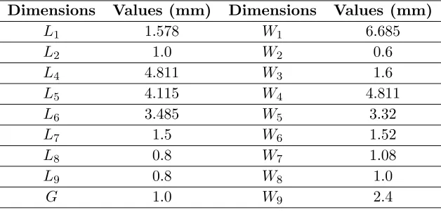
Table 1. Dimensions of SIR-LPF&DMS.
Dimensions Values (mm) Dimensions Values (mm)
L1 1.578 W1 6.685
L2 1.0 W2 0.6
L4 4.811 W3 1.6
L5 4.115 W4 4.811
L6 3.485 W5 3.32
L7 1.5 W6 1.52
L8 0.8 W7 1.08
L9 0.8 W8 1.0
G 1.0 W9 2.4
constructed by vertical and horizontal thin slots which act as capacitance and inductance consequently. The T-shaped DMS design has a neck dimension of (W2 ×L2/2) and foot dimension of (W3×L2/2) as shown in Fig. 1. The effective capacitance increases as W2 and W3 increase, while the effective inductance decreases as W2 and W3 increase.
The microstrip technology with defected ground structure is proposed to enhance the performance of the filter in the stopband. DGS is realized by etching simple defected shapes in the ground plane. The different defected shapes alter the currant distribution paths in the ground plane. This disturbance can vary characteristics of the filter to a better performance. Any microstrip distributed defect (slot) in the ground plane is equivalent to a resistance, effective inductance, and effective capacitance [4]. Among all different DGS shapes, a dumbbell-shaped defected ground structure (DB-DGS) shown in Fig. 1(b) is proposed to achieve compact size and wide stopband. The current path is increased according to rectangular sections of the dumbbell DGS. Table 2 lists the dimensions of the DB-DGS in the ground plane, which is located at distance X = 3.2 mm from the filter structure edge. Increasing the dimensions ofy2 and y1 can increase the effective capacitance, but decreasing the dimensions ofx2 and
x1 can increase the effective inductance. Also the change of distanceX affects the attenuation in the stopband. The simulated scattering parameters of the filter without surface mount capacitor are shown in Fig. 2. It is clear that the filter has high insertion loss in passband, no sharp transition, and low stopband attenuation. In addition, the filter has high cutoff frequency fc= 3.3138 GHz.
Table 2. Dimensions of DB-DGS.
Dimensions Values (mm) Dimensions Values (mm)
x1 0.8 y1 4.0
x2 1.7 y2 1.8
x3 0.7 y3 1.2
x4 0.8 y4 0.8
x5 1.2 X 3.2
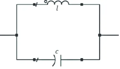
The L-C equivalent circuit of the DB-DGS is shown in Fig. 3 [8]. The DB-DGS lumped elements values derived from ADS software are c4 =c5 = 0.35 PF and l4 =l5 = 1.55 nH. Using this DB-DGS equivalent circuit, the L-C equivalent circuit of the filter will be as shown in Fig. 4. According to butterworth lowpass prototype filter [1, 8], the lumped elements values using a transmission line of characteristic impedance Z0 = 50 Ω are l1 = 3.836 nH, l2 = 9.77 nH, l3 = 9.283 nH, c1 = 3.09 PF,
Figure 2. Scattering parameters of the filter without surface mount capacitor.
Figure 3. Equivalent circuit for DB-DGS cell.
Figure 4. Equivalent circuit of the filter without surface mount capacitor using ADS.
2.2. Filter Design Using Surface Mount Capacitor
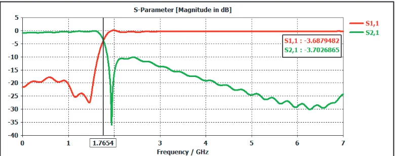
To enhance the previous filter characteristics, a surface mount capacitor is added to the design as shown in Fig. 6. The surface mount capacitor is located on the surface of the SIR filter design at the middle of L5 dimension. Adding a surface mount capacitor of (1.0 PF) increases the effective capacitance of the filter and enhances characteristics of the filter. The simulated scattering parameters of the filter are shown in Fig. 7. The filter cutoff frequency is greatly reduced to fc = 1.7654 GHz instead of
Figure 5. Scattering parameters of the filter without surface mount capacitor using ADS simulator.
Figure 6. The proposed DB-DGS low pass filter using surface mount capacitor.
Figure 7. Simulated scattering parameters of the proposed filter using surface mount capacitor.
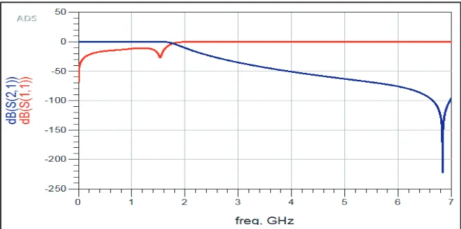
Figure 8. Equivalent circuit of the proposed filter using surface mount capacitor derived from ADS.
Figure 9. Scattering parameters the proposed filter with surface mount capacitor using ADS simulator.
Figure 10. Comparison between EM simulations of the proposed filter with surface mount capacitor and the LPF filter introduced in [2].
Table 3. Comparison between the proposed LPF and the LPF introduced in [2].
Dimensions (m2) Insertion loss Cut-off frequency The LPF
introduced in [2] 20×25 0.5 dB 2.635 GHz The proposed
LPF 20×16 0.15 dB 1.7654 GHz
Table 4. Additional comparisons between the proposed LPF and other related works.
Ref. Substrate dielectric constant/height (mm) Insertion loss (dB) Cut-off frequency (GHz) Stopband (GHz @ dB)
Dimensions (mm2)
[2] 2.65/0.5 <0.5 2.5 (2.58 to 7.5 @20) 20×16 [3] 3.38/2.0 <0.37 2.28 (2.42 to 14.9 @20) 19.8×11
[5] 3.2/1.524 0.2 2.4 (2.6 to 7.0 @20) 29×20
[6] 2.2/1.0 <1.0 2.5 (2.9 to 6.5 @40) 27×20
[10] 4.4/1.59 0.6 2.5 (3.6 to 6 @40) 40×14
This
work 2.65/0.5 <0.15 1.7654 (1.9 to 7.0 @10) 20×16
introduced in [2]. Furthermore, the proposed filter has very low insertion loss equal to 0.15 dB while the other filter has high insertion loss equal to 0.5 dB. It means that the proposed filter provides better passband characteristics than the LPF introduced in [2]. Additional comparisons between the proposed filter and previous related works are presented in Table 4. It is clear that the proposed filter exhibits the lowest cutoff frequency and the smallest insertion loss.
For the third order butterworth microstrip LPF design, the effective capacitance C and effective inductance Lare given by Eq. (1) and Eq. (2), respectively [14].
C = fc
2πZ0
f2 0 −fc2
(1)
L = 1
4π2f2 0C
(2)
where fc is the 3 dB cutoff frequency, f0 the resonant frequency of the attenuation pole, and Z0 the characteristic impedance of the microstrip line. Using the equivalent circuit of the proposed filter shown in Fig. 8, the effective capacitance and effective inductance deduced from ADS software are found to be C = 0.04163718 F and L = 0.1689111 H, respectively. From Eq. (2), the calculated resonance frequency equalsf0= 1.881 GHz. Applying this result in Eq. (1), the calculated cutoff frequency equals
fc = 1.79 GHz which is very close to the measurements using the Network Analyzer.
3. FABRICATION AND MEASUREMENT OF THE PROPOSED LPF
(a) (b)
Figure 11. (a) Photograph of the back view for the fabricated prototype of the proposed filter, (b) photograph of the front view for the fabricated prototype of the proposed filter.
Figure 12. Measurement of the fabricated LPF filter using Rohde & Schwarz ZVL20 Network Analyzer.
4. CONCLUSION
In this paper, a new design for a compact microstrip LPF with low insertion loss is introduced. The filter is based on SIR, DMS, DGS, and surface mount capacitor techniques. The filter is fabricated on an F4B-2 substrate with relative dielectric constantεr = 2.65, thicknessh= 0.5 mm and loss tangentδ= 0.0013. The filter design is performed using CST-Microwave Studio software, and the filter equivalent circuit is derived using ADS2006A software. |S11|and|S21|parameters of the fabricated filter are measured using Rohde & Schwarz ZVL20 Network Analyzer. The filter exhibits sharp cutoff frequency which equals 1.7654 GHz and very low insertion loss about 0.15 dB. In addition, it has a compact size of 20×16 mm2). The results reveal that the simulated and measured parameters are in very good agreement.
REFERENCES
1. Hong, J. S. and M. J. Lancaster, Microstrip Filters for RF/Microwave Applications, John Wiley and Sons, New York, 2001.
2. Xi, D., Y.-Z. Yin, L.-H. Wen, Y. Mo, and Y. Wang, “A compact low-pass filter with sharp cut-off and low insertion loss characteristic using novel defected ground structure,” Progress In Electromagnetics Research Letters, Vol. 17, 133–143, 2010.
3. Al-Din Makki, S. V., A. Ahmadi, S. Majidifar, H. Sariri, and Z. Rahmani, “Sharp response microstrip LPF using folded stepped impedance open stubs,” Radio Engineering, Vol. 22, 328– 332, 2013.
4. Mukesh, K. K., K. K. Binod, and K. Sachin, “Defected ground structure: fundamentals, analysis, and applications in modern wireless trends,” Hindawi International Journal of Antennas and Propagation, Vol. 2017, 1–23, 2017.
5. Kumar, A., H. Alavi, J. A. Mix, E. C. Beltran, E. C. Perez, A. J. Vera, and H. V. Cruz, “Design of nine pole microstrip low pass filter with metal loaded defected ground structure,”IEEE MTT-S Latin America Microwave Conference (LAMC-2016), 12–14, Puerto Vallarta, Mexico, 2016. 6. Ning, J., L. Chen, C. Zeng, and S. Bu, “A compact elliptic-function low-pass filter using
stepped-impedance coupled microstrip resonators,” IEEE Microwave, 1557–1562, 2014.
7. Belbachir, A. K., M. Boussouis, and N. Amar Touhami, “High-performance LPF using coupled C-shape DGS and radial stub resonators for microwave mixer,”Progress In Electromagnetics Research Letters, Vol. 58, 97–103, 2016.
8. Arjun, K. and M. V. Kartikeyan, “Design and realization of microstrip filters with new defected ground structure (DGS),” Engineering Science and Technology, An International Journal, Vol. 20, 679–686, 2017.
9. Mondal, P., H. Dey, and S. K. Parui, “Design of microstrip lowpass filter in combination with defected ground and defected microstrip structures,” Computational Advancement in Communication Circuits and Systems, Lecture Notes in Electrical Engineering, Vol. 335, 61–66, Springer, New Delhi, 2015.
10. Ahmed, B., A. I. Ahmed, and P. B. Edmund, “Design of a novel ultrawide stopband lowpass filter using a DMS-DGS technique for radar applications,” International Journal of Microwave Science and Technology Hindawi Publishing Corporation, Vol. 2015, 1–7, 2015.
11. Packiaraj, D., K. J. Vinoy, M. Ramesh, and A. T. Kalghatgi, “Design of compact low pass filter with wide stop band using tri-section stepped impedance resonator,” Int. J. Electron. Commun. (AE ¨U), Vol. 65, 1012–1014, 2011.
12. Kumud, R. J. and R. Manish, “Modification in microstrip low pass filter using bulb shape patch,”
Int. J. Electron. Commun. (AE ¨U), Vol. 63, 1076–1079, 2009.

![Table 3. Comparison between the proposed LPF and the LPF introduced in [2].](https://thumb-us.123doks.com/thumbv2/123dok_us/1975527.1260846/7.612.70.549.228.376/table-comparison-proposed-lpf-lpf-introduced.webp)
