Available Online at www.ijcsmc.com
International Journal of Computer Science and Mobile Computing
A Monthly Journal of Computer Science and Information Technology
ISSN 2320–088X
IJCSMC, Vol. 3, Issue. 10, October 2014, pg.483 – 496
RESEARCH ARTICLE
PHOTOVOLTAIC BASED HIGH-EFFICIENCY
SINGLE-INPUT MULTIPLE-OUTPUT DC-DC CONVERTER
J.Kondalaiah
1 M.Tech1I.Rahul
2M.Tech, Assistant Professor2 Vignana Bharathi Institute of Technology12
ABSTRACT: The aim of this paper is to develop a photo voltaic power generation based high-efficiency multiple-output dc–dc converter. The proposed converter can boost the voltage of a low-voltage input power source to a controllable high-voltage dc bus and middle-voltage output terminals. In this paper, a coupled-inductor based dc–dc converter scheme utilizes only one power switch with the properties of voltage clamping and soft switching, and the corresponding device specifications are adequately designed. As a result, the objectives of high-efficiency power conversion, high step up ratio, and various output voltages with different levels can be obtained.
I. INTRODUCTION
The development of new energy sources is continuously enhanced because of the critical situation
of the chemical industrial fuels such as oil, gas and others. Thus, the renewable energy sources have
become a more important contributor to the total energy consumed in the world. In fact, the demand
for solar energy has increased by 20% to 25% over the past 20 years [1]. The market for PV systems
is growing worldwide. In fact, nowadays, solar PV provides around 4800 GW. Between 2004 and
2009, grid connected PV capacity reached 21 GW and was increasing at an annual average rate of
60% [2]. In order to get benefit from the application of PV systems, research activities are being
Typically, a PV cell generates a voltage around 0.5 to 0.8 volts depending on the semiconductor and
the built-up technology. This voltage is low enough as it cannot be of use. Therefore, to get benefit
from this technology, tens of PV cells (involving 36 to 72 cells) are connected in series to form a PV
module. These modules can be interconnected in series and/or parallel to form a PV panel. In case
these modules are connected in series, their voltages are added with the same current. Nevertheless,
when they are connected in parallel, their currents are added while the voltage is the same.
The newly designed multi output converter with a coupled inductor. The proposed converter uses one
power switch to achieve the objectives of high-efficiency power conversion, high step-up ratio, and
different output voltage levels. In the proposed multi output converter, the techniques of soft
switching and voltage clamping are adopted to reduce the switching and conduction losses via the
utilization of a low-voltage-rated power switch with a small RDS(on). Because the slew rate of the
current change in the coupled inductor can be restricted by the leakage inductor, the current transition
time enables the power switch to turn ON with the ZCS property easily, and the effect of the leakage
inductor can alleviate the losses caused by the reverse-recovery current.
The voltages of middle-voltage output terminals can be appropriately adjusted by the design of
auxiliary inductors; the output voltage of the high-voltage dc bus can be stably controlled by a simple
proportional-integral (PI) control.
II. CONVERTER DESIGN AND ANALYSES
The system configuration of the proposed high-efficiency SIMO converter topology to generate two
different voltage levels from a single-input power source is depicted in Fig. 1. This SIMO converter
contains five parts including a low-voltage-side circuit (LVSC), a clamped circuit, a middle-voltage
circuit, an auxiliary circuit, and a high-voltage-side circuit (HVSC). The major symbol representations
are summarized as follows. VFC (iFC) and VO1 (iO1 ) denote the voltages (currents) of the input power
source and the output load at the LVSC and the auxiliary circuit, respectively; VO2 and iO2 are the
output voltage and current in the HVSC. CFC, CO1 , and CO2 are the filter capacitors at the LVSC, the
The main switch is expressed as S1 in the LVSC; the equivalent load in the auxiliary circuit is
represented as RO 1, and the output load is represented as RO 2 in the HVSC.
Fig 1.circuit configuration of multi output converter
The corresponding equivalent circuit given in Fig. 2 is used to define the voltage polarities and
current directions. The coupled inductor in Fig. 1 can be modeled as an ideal transformer including
the magnetizing inductor Lmpand the leakage inductor Lkpin Fig. 2. The turns ratio N and coupling
coefficient k of this ideal transformer are defined as
N = N2/N1 ………..(1)
k = Lmp/ (Lkp + Lmp) = Lmp/LP ………(2)
whereN1 and N2 are the winding turns in the primary and secondary sides of the coupled inductor
Tr. Because the voltage gain is less sensitive to the coupling coefficient and the clamped capacitor
C1 is appropriately selected to completely absorb the leakage inductor energy, the coupling
Fig 2.eqivalant circuit
In this paper, the following assumptions are made to simplify the converter analyses: 1) The main
switch including its body diode is assumed to be an ideal switching element; and 2) The conduction
voltage drops of the switch and diodes are neglected.
The major advantages of proposed dc-dc converter as follows: 1) this topology adopts only one
power switch to achieve the objective of high-efficiency SIMO power conversion; 2) the voltage
gain can be substantially increased by using a coupled inductor; 3) the stray energy can be recycled
by a clamped capacitor into the auxiliary battery module or high-voltage dc bus to ensure the
property of voltage clamping; 4) an auxiliary inductor is designed for providing the charge power
to the auxiliary battery module and assisting the switch turned ON under the condition of ZCS; 5)
the switch voltage stress is not related to the input voltage so that it is more suitable for a dc power
conversion mechanism with different input voltage levels; and 6) the copper loss in the magnetic
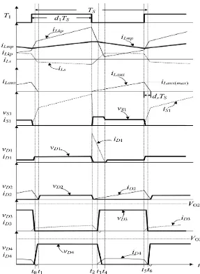
Fig 3.charecterisitc wave form of proposed converter
III.Mathematical Model of PV cell
A general mathematical description of I-V output characteristics for a PV cell has been studied for
over the pass four decades. Such an equivalent circuit-based model is mainly used for the MPPT
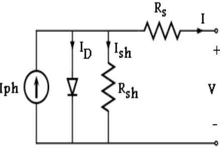
technologies [3,4,5,6]. The equivalent circuit of the general model which consists of a photo
current, a diode, a parallel resistor expressing a leakage current, and a series resistor describing an
internal resistance to the current flow, is shown in Fig.1. The voltage-current characteristic equation
Where
Iph is a light-generated current or photocurrent,
Is is the cell saturation of dark current,
q(= 1.6 ×10⁻¹⁹ C) is an electron charge,
k(= 1.38 ×10⁻²³J/K) is a Boltzmann’s constant,
Tc is the cell’s working temperature,
A is an ideal factor,
Rsh is a Sunt resistance, and
Rs is a series resistance of solar cell
Fig. 4.PV cell equivalent circuit
The photocurrent mainly depends on the solar insolation and cell’s working temperature, which is
described as
where
Isc is the cell’s short-circuit current at a 25°C and 1kW/m2,
KI is the cell’s short-circuit current temperature coefficient,
Tref is the cell’s reference temperature, and
IV.SIMULATION RESULTS
The proposed PV –based single input multi output converter system with single stage power
conversion is simulated with MATLAB/SIMULINK (7.8 R 2009Aversion) environment
Fig 5.Complete Simulink model for proposed converter
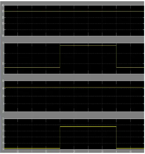
Fig 7.voltage and current responses of proposed converter with 200-W output power
Fig 7 shows the input voltage, input current, output voltage at terminal1 and output voltage at
terminal2.input voltage is from solar panel which is 24 volts and input current is 9.5amperes.outut
voltage at terminal1 is 44 volts and output voltage at terminal2 is 300volts.Fig 8 shows the
switching voltage and switching current of proposed converter with 200-W output power. These
wave forms show effectiveness of switching pulses with less distortion. The switching frequency is
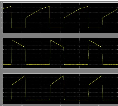
100 kHz. Fig 9 shows the leakage current, secondary current, auxiliary current responses of
Fig 8.switch voltage and switch current responses of proposed converter with 200-W output power
Fig 10.voltage and current responses of proposed converter with 800-W output power
Fig 12.leakage, secondary, auxiliary current responses of proposed converter with 800-W output power
Fig 10 shows the input voltage, input current, output voltage at terminal1 and output voltage at
terminal2.input voltage is from solar panel which is 24 volts and input current is 38 amperes. output
voltage at terminal1 is 44 volts and output voltage at terminal2 is 300volts. Fig 11 shows the
switching voltage and switching current of proposed converter with 800-W output power. These
wave forms show effectiveness of switching pulses with less distortion. The switching frequency is
100 kHz.Fig 12 shows the leakage current, secondary current, auxiliary current responses of
Fig 13.proposed converter response during output power change from 125w to 550w
Figure 13 shows the output voltage at terminal 2 is 300 volts, output current at load terminal2 is
varies from 0.32amperes to 1.4 amperes during load power change. output voltage at terminal 1 is
40 volts and output current at load terminal1 is varies from 1.4 amperes to 1.8 amperes during load
power change.
V. CONCLUSION
This study has successfully developed a photovoltaic power generation based high-efficiencymulti
output dc–dc converter, and this coupled-inductor-based converterwas applied well to a
single-input power source plustwo output terminals composed of an auxiliary battery moduleand a
high-voltage dc bus. This high-efficiency dc-dc converter topology provides designerswith an alternative
choice for boosting a low-voltagepower source to multiple outputs with different voltage
levelsefficiently.
Appendex
CO2 = 20 μF/250 V;
Input power source = 24V
Auxiliary output voltage VO1 = 42 – 44V
Desired output voltage Vcmd = 300V
Switching frequency fS= 100 kHz;
Coupled inductor LP = 3 μH; LS = 75 μH;
Auxiliary inductor Laux = 2 μH;
REFERENCES
[1]P. Patra, A. Patra, and N. Misra, “A single-inductor multiple-output switcher with simultaneous buck, boost and inverted outputs,” IEEETrans. Power Electron., vol. 27, no. 4, pp. 1936–1951, Apr.
2012.
[2] A. Nami, F. Zare, A. Ghosh, and F. Blaabjerg, “Multiple-output DC–DC converters based on
diode-clamped converters configuration: Topology and control strategy,” IET Power Electron., vol.
3, no. 2, pp. 197–208, 2010.
[3] Y. Chen, Y. Kang, S. Nie, and X. Pei, “The multiple-output DC–DC converter with shared
ZCS lagging leg,” IEEE Trans. Power Electron., vol. 26, no. 8, pp. 2278–2294, Aug. 2011.
[4]R. J.Wai and R. Y. Duan, “High step-up converter with coupled inductor,” IEEE Trans. Power
Electron., vol. 20, no. 5, pp. 1025–1035, Sep. 2005.
[5] N. Mohan, T. M. Undeland, and W. P. Robbins, Power Electronics: Converters, Applications,
and Design. New York: Wiley, 1995.
[6] L. Schuch, C. Rech, H. L. Hey, H. A. Gr¨undling, H. Pinheiro, and J. R. Pinheiro, “Analysis and
design of a new high-efficiency bidirectional integrated ZVT PWM converter for DC-bus and
battery-bank interface,” IEEE Trans. Ind. Appl., vol. 42, no. 5, pp. 1321–1332, Sep./Oct. 2006.
[7] Y. Chen and Y. Kang, “A full regulated dual-output dc-dc converter with special-connected two
transformers (SCTTs) cell and complementary pulsewidth modulation-PFM(CPWM-PFM),” IEEE
Trans. PowerElectron., vol. 25, no. 5, pp. 1296–1309, May 2010.
[8] R. Faranda and S. Leva, "Energy Comparison of MPPT techniques for PV Systems," WSES
J.Kondalaiah Mtech Scholar Department Of EEE Vignana Bharathi Institute Of Technology, Ghatkesar. B.Tech In Nova College Of Engineering And Technology Area Of Interests Are Power Electronics, Electrical Drives.