1Graduate Institute of Mechatronic Engineering, National Taipei University of Technology, Taipei 10608, Taiwan. 2Department of Electronic Engineering, Minghsin University of Science and Technology, Hsinchu 30401, Taiwan. 3Department of Materials and Resources Engineering, National Taipei University of Technology, Taipei 10608, Taiwan. 4Reliability Technology and Assurance Division, United Microelectronics Corporation, Hsinchu 30078, Taiwan.
*Correspondence author: [email protected]
Abstract—A novel drive current model covering the effects of source/drain voltage (VDS) and gate voltage (VGS) and incorporating drift and diffusion current on the surface channel at the nano-node level, especially beyond 28nm node is presented. The effect of the diffusion current added is more satisfactory to describe the behavior of the drive current in nano-node MOSFETs, fabricated with the atomic-layer-deposition (ALD) technology. This breakthrough in model establishment can expose the long and short channel devices together. Introducing the variables of VDS and VGS, the mixed current model more effectively and meaningfully demonstrates the drive current of MOSFETs under the operation of horizontal, vertical, or mixed electrical field. In comparison between the simulation and experimental consequences, the electrical performance is impressive. The error between both is less than 1%, better than the empirical adjustment to issue a set of drive current models.
Index Terms—drift current, diffusion current, mobility, nano-node, model, ALD technology.
I. INTRODUCTION
In conventional device models for metal-oxide-semiconductor field-effect transistors (MOSFETs), the drive current [1,2] mainly considers the moving carriers with the drift effect. As the channel length of MOSFET keeps scaling down, the saturation current of MOSFETs raises up with the increase of the drain voltage or the decrease of the channel length. There are some published literatures to explain this phenomenon, such as channel length modulation [3-5] and velocity overshoot [6-9]. However, the proposed conduction mechanisms seem not fully to fit the physically measured current-voltage results well. To compensate this drawback, the device models in semiconductor foundries usually assist some empirical adjustment, but no physical meanings. Here, we propose a new concept incorporating the diffusion effect in each channel point due to the gradient of inversion charge density, especially near the pinch-off point. At this point, the inversion charge density traditionally approaches to zero, indicating the drift current zero, but the real drive current is not zero.
As a result, the drive current rises as the drain voltage increases for a nano-scale MOSFET. Adding the diffusion effect in drive-current model, the contribution of diffusion current in entire drive current is distinctly enhanced, especially in the current behavior of short channel devices [10]. In other words, a lager source/drain voltage VDS will make a lager gradient of inversion charge density causing a larger surface diffusion current.
However, the previous work only changing one parameter (VDS) as VGS fixed in long or short channel devices
to fit the equivalent mobility μeq accurately was successfully finished. In this work, we furthermore propose
a deeper consideration incorporating the modulation of all the parameters (VDS, VGS and Lmask) at one time
to fit μeq correlated to VDS, VGS and channel length on drawn mask Lmask. Furthermore, consolidating the
adjustment of VDS and Lmask correlated to the horizontal electric field and VGS influencing the vertical electric
field, the drive current of MOSFETs is more meaningful and beneficial in providing a set of accurate
nano-The Mixed Current Model of Nano-MOSFETs
Considering the Effect of Horizontal and
Vertical Electric Fields
Heng-Sheng Huang
1, Ping-Ray Huang
1, Mu-Chun Wang
1,2,*, Shuang-Yuan
Chen
1, Shea-Jue Wang
3, Ching-Chuan Chou
2, LS Huang
4, Wei-Lun Wang
1node device models, especially beyond 28nm node. The gate dielectric in this work was the sandwich stack of HfOx/ZrOy/HfOz deposited with the atomic layer deposition (ALD) technology. The physical thickness
with ALD technology is about 24Å
II. II. EXPERIMENTAL AND FITTING THE MOBILITY
Based on the previous work [10], the carrier mobility μ(x) should be the function of the position x in the surface channel. But it seems not enough to describe the whole behavior of an equivalent mobility μeq
correlated to VDS, VGS, and Lmask, independent of the position x. Incorporating the various conditions with
VDS, VGS and Lmask is to reasonably describe the whole drive current and fit the μeq as shown in Eqs. (1)-(4):
𝐼 = 𝑄 (𝑥) × 𝜈 (𝑥) × 𝑊 (1)
𝐼 = 𝐷 × ( )× 𝑊 ; 𝐷 = 𝜇 × 𝑘𝑇 𝑞 (2)
= 𝐼 + 𝐼 = −𝑄 (𝑥) × 𝜈 (𝑥) + 𝐷 × ( ) (3)
= −µ ( )
( )
( ) + 𝐷 ×
( )
(4)
where q: unit charge, W: channel width, νd: carrier drift velocity, Dn: diffusion coefficient of electron carrier,
Esat: horizontal electric field in saturation, k: Boltzmann constant, T: absolute temperature, and m: body
factor.
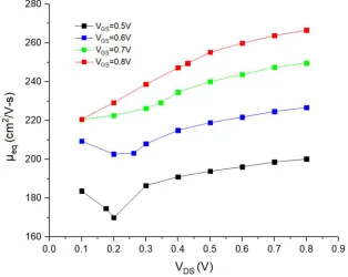
Under the specific conditions such as fixing a channel length and tuning the gate voltages to sense the IDS
-VDS characteristics, we can derive the relationship between the μeq and the drain bias, as shown in Fig. 1.
Through changing the fixed channel length and the drain bias, the linear and saturation regions are obviously represented no matter what the tested channel device is. It is important to seek the accurate relationship between these three parameters and the μeq. In this work, there are four sections (a, b, c, d) illustrating
long-short channel devices and linear-saturation regions split at Lmask = 120 nm due to the classification of
electrical measurement, as shown in Table I.
Preprints (www.preprints.org) | NOT PEER-REVIEWED | Posted: 11 February 2019
Fig. 1. μeq vs. VDS under different VGS at Lmask =500 nm in section a.
Table I. Four sections classified as long-short devices and linear-saturation regions. Long channel (>120 nm), Linear region X=a
Long channel (>120 nm), Saturation region X=b Short channel (< 120 nm), Linear region X=c Short channel (< 120 nm), Saturation region X=d
First, the μeq can be written as a function of VDS in different VGS at fixed Lmask, which can be described by
the Taylor expansion until the third-order polynomial, as shown in Eq.(5):
𝜇 (𝑉 ) = ∑ 𝑋 × (𝑉 ) (5)
where Xi is the coefficient of the ith polynomial and i=0,1,2,3. X can be attributed as each section (a, b, c, or
d).
Continuously, the Xi is strongly related to the gate voltages as Lmask fixed, which can be given as Eq.(6)
with the Taylor expansion.
𝑋 (𝑉 ) = ∑ 𝑋 × (𝑉 ) (6)
where Xij is the coefficient of VGS polynomials with j=0,1,2,3.
Ultimately, the impact factor Lmask to the coefficient Xij is entirely represented as Eq.(7):
𝑋 (𝐿 ) = ∑ 𝑋 × (𝐿 ) (7)
where Xijk is the coefficient of Lmask variable with k=0,1,2.
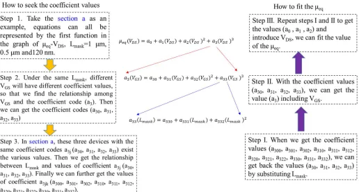
The flow chart of X-coefficients and the μeq value in extraction is demonstrated in Fig.2 with section a as
an example. The other sections in parameter extraction also follow the same procedures to achieve the accurate μeq value correlated to VDS, VGS, and Lmask variables. Table II demonstrates the full relationship of
Fig. 2. The flow chart for extracting the coefficients and μeq values with section a as an example.
Table II. The relationship among each parameter and the coefficient in Taylor expansion. The coefficient of μeq (VDS) Xi : the functions of VGS ,
i=0, 1, 2, 3
The coefficient of Xi (VGS) Xij : the functions of Lmask,
j=0, 1, 2, 3
The coefficient of Xij (Lmask) Xijk : constant, k=0, 1, 2
III. III. RESULTSANDDISCUSSION
Following the last flow chart to obtain the coefficients (Xi, Xij, Xijk), the μeq(VDS, VGS, Lmask) at any condition
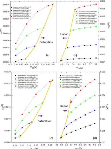
can be effectively and meaningfully extracted. After that, the equivalent mobility will be immediately substituted into (4) to do the simulation of the corresponding drive current. The simulation and experimental results of I-V curves with long and short channel devices represented as four sections are shown in Fig. 3. Preprints (www.preprints.org) | NOT PEER-REVIEWED | Posted: 11 February 2019
Fig. 3. IDS vs. VDS curves for long-channel devices: (a) at Lmask= 1 μm in section a and (b) at Lmask= 500 nm
in section b; for short-channel devices: (c) at Lmask= 50 nm in section c and (d) at Lmask= 33 nm in section d.
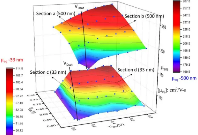
For precise observation of the contribution of the μeq correlated to VDS, VGS, and Lmask, one 3-D plot is
established and shown in Fig. 4, combining all of these extracted data linked as lines and extended these lines as a continuous plane.
In this study, the tested channel-length devices contain 33, 50, 90, 120, 500 nm and 1 μm. As the channel length L is greater than 120 nm, the section is defined as the long-channel section. Thus, the plot in Fig.4 with L= 500 nm is represented as long-channel section and with L= 33 nm as short-channel one. Furthermore, the VDS and VGS sensed are 0.1, 0.2…, 0.8 V and 0.5, 0.6, 0.7, 0.8 V, respectively. The error between
operation mode at linear or saturation region are. Table III is an example to extract the coefficients in section a under VGS= 0.8 V and Lmask= 500 nm.
Fig. 4. Three dimensions of μeq versus VDS and VGS at Lmask =500 nm (long-channel) and 33 nm
(short-channel).
Table III. The values of coefficients in section a under VGS= 0.8 V and Lmask = 500 nm.
The value of a3 a3= -247.999
The values of a3j
a33= 19833.33
a32= -5150
a31= -29383.3
a30= 16400
The values of a3jk
a332= -3283858.592 a331= 5452922.151 a330= -1885663.094 a322= 6422679 a321= -10725100.45 a320= 3751730.477 a312= -4094362.073 a311= 6889789.134 a310= -2450687.382 a302= 840872.7189 a301= -1430708.191 a300= 521535.9158
IV. IV. CONCLUSION
Without considering the effect of channel length modulation and drift velocity overshoot, the mixed current model, including surface drift and diffusion current, has been announced to describe the electrical behavior of drive current of nano-node MOSFETs. The existence of diffusion current addresses why the drive current enters the saturation region, but not zero at the pinch-off point. The diffusion contribution in drive current becomes more apparent, especially for short-channel MOSFETs. For devices in normal operation, the Preprints (www.preprints.org) | NOT PEER-REVIEWED | Posted: 11 February 2019
parameters (VDS, VGS, and Lmask) independent of channel poistion are strongly correlated to the μeq value.
Investigating the mutual interaction among them is indeed necessary. This work successfully provides the physical and meaningful consequences for nano-node MOSFET devices, fabricated with the ALD technology. The error between simulation and experimental results is less than 1%, which is more suitable to the 28nm devices or beyond to build up a more accurate set of device model in circuit design consideration.
ACKNOWLEDGEMENT
This work was supported in part by the Chung-Shan Institute of Science and Technology in Taiwan under Grant NCSIST-1164-V101 (106). The authors sincerely thank UMC in Taiwan provides the great 28-nm node logic wafers in this research.
REFERENCES
[1] B.G. Streetman, S.K. Banerjee, Solid state electronic devices. 7th ed., Pearson, New Jersey, USA, 2016, pp.290-350.
[2] C. Hu, Modern semiconductor devices for integrated circuits. 1st ed., Pearson, New Jersey, USA, 2010, pp.213-265.
[3] C. Nguyen-Duc, S. Cristoloveanu, G. Ghibaudo, “A three-piece model of channel length modulation in submicrometer MOSFETs,” Solid-State Electronics, vol.31, iss.6, pp.1057-1063, 1988.
[4] K.Y. Lim, X. Zhou, “An analytical effective channel-length modulation model for velocity overshoot in submicron MOSFETs based on energy-balance formulation,” Microelectronics Reliability, vol.42, iss.12, pp.1857-1864, 2002. [5] B.J. Moon, C.K. Park, K. Lee, M. Shur, “New short-channel n-MOSFET current-voltage model in strong inversion and
unified parameter extraction method,” IEEE Trans. Electron Dev., vol.38, iss.3, pp.592-602, 1991.
[6] G.G. Shasidl, D. A. Antoniadis, H. I. Smith, “Electron velocity overshoot at room and liquid nitrogen temperatures in silicon inversion layers,” IEEE Electron Dev. Lett., vol.9, iss.2, pp.94-96, 1988.
[7] K. K. Thornber, “Current equations for velocity overshoot,” IEEE Electron Dev. Lett., vol.3, iss.3, pp.69-71, 1982. [8] T. Kobayashi, K. Saito, “Two-dimensional analysis of velocity overshoot effects in ultrashort-channel Si
MOSFET's,” IEEE Trans. Electron Dev., vol.32, iss.4, pp.788-792, 1985.
[9] S. Y. Chou, D. A. Antoniadis, H. I. Smith, “Observation of electron velocity overshoot in sub-100-nm-channel MOSFET's in silicon,” IEEE Electron Dev. Lett., vol.6, iss.12, pp.665-667, 1985.