Linearization of RF Power Amplifiers
by
Mark A. Briffa.
A thesis submitted for the degree of
Doctor of Philosophy
at
Victoria University of Technology
December, 1996.
Department of Electrical and Electronic Engineering BOX 14428 MCMC
ATTENTION
This thesis entitled, “Linearization of RF Power Amplifiers” was submitted in December, 1996, and has been converted into electronic form by the author in 2001.
This thesis has been made available to interested parties in good faith, such that no part of the thesis may be copied or printed for commercial gain without prior consent from the author. This copy however can be freely read and distributed.
Comments and queries regarding this work can be directed to the author: markbriffa@yahoo.com
Statement of Originality
I hereby certify that the work contained in this thesis is the result of original research (except where due reference is given) and has not been submitted for a higher degree to any other university or institution.
This thesis may be made available for consultation within the Victoria University Library and may be photocopied or lent to other libraries for the purposes of consultation.
A
BSTRACT
Linearization of RF power amplifiers is surveyed, reviewed and analyzed. Cartesian feedback is specifically presented as an effective means of linearizing an efficient yet non-linear power amplifier. This reduces amplifier distortion to acceptable levels and enables the transmission of RF signals utilizing spectrally efficient linear modulation schemes with a lower consumption of DC power. Results from constructing experimental hardware shows an intermodulation distortion (IMD) reduction of 44dB (achieving a level of −62dBc) combined with an efficiency of 42% when transmitting π/4 QPSK. The careful amplifier characterization measurement method presented predicts performance to within 2dB (IMD) and 4% (efficiency) of practical measurements when used in simulations.
region when the phase adjuster is adjusted above optimum, and instability also results at transistor saturation when adjusted lower than optimum. This is also demonstrated with experimental hardware.
From the analysis, the perturbated behaviour of the non-linear piecewise amplifier model is shown to display two forms of operation when placed in a feedback loop, namely: spiral mode and stationary mode. Spiralling tends to cause the noise floor of the output spectrum to rise on one side depending on the direction of the spiral. The direction is in turn dependent on the setting of the RF phase adjuster within the loop. When the phase adjuster is in the forward path, phase adjustments lower than optimum, will cause the noise to rise on the right side of the output spectrum (anti-clockwise spiralling) and vice-versa. With the phase adjuster in the feedback path the reverse is true.
Loops with low stability margins are demonstrated to exhibit closed-loop peaking which can affect the out of band noise performance of a cartesian feedback transmitter. In order to achieve a non-peaking condition for a first order loop with delay, the phase margin of the loop needs to be around 60°. It is also possible to approximately predict the degree of peaking from the gain and phase margins. Further investigation of noise performance suggests the loop compensation should be placed as far up the forward chain as possible (i.e. close to the power amplifier) in order to minimize the out-of-band noise floor. This too is demonstrated experimentally.
The concept of dynamic bias is also presented as a method to improve cartesian feedback efficiency. The method works by setting up optimum bias conditions for the power amplifier (derived from amplifier characterizations) and then having the cartesian feedback loop make fine adjustments to the RF drive to achieve the exact required output. This way the bias conditions do not have to be applied perfectly, implying simple (i.e low switching frequency) switched mode power supplies can be used to apply the desired collector voltage for example. The simple step-down switch mode power supply constructed achieved an efficiency of 95% at high output levels. Applying it to a cartesian
feedback loop markedly improved efficiency. At an output power of 20dBm average, the linearized amplifier efficiency lifted from 45% to 67%, an improvement of over 20% and a reduction in current consumption by 33%.
P
REFACE
In this thesis I present my work in Linearization of RF Power Amplifiers. The work primarily examines cartesian feedback as the means by which efficient yet non-linear RF (radio frequency) power amplifiers can be linearized over a narrow bandwidth.
Linearization, or the reduction of distortion in electronic systems, has been a goal for electronic engineers for as long as electronics has existed. Feedback has had widespread and successful application to achieve this end. In recent times, the need for linear RF power amplifiers has been spurred on by the demands of cellular and wireless communications to carry more traffic over a given spectrum. As I present in chapter 1, this has led to the increased use of spectrally efficient modulation schemes. These schemes have modulation on the envelope and hence require linear RF power amplifiers in the transmitter. Other applications for linear RF power amplifiers are also discussed in this introductory chapter.
In chapter 2, I collated background material which surveys the field of RF power amplifier linearization as it applies to modern transmitter architectures. The non-linear aspects of the RF power amplifier are presented and the consequences of such non-linearities and distortions are shown. A number of linearization methods can reduce these distortions with varying degrees of success and these are reviewed with my comments.
The rest of the thesis represents a summary of the work I performed in the area of cartesian feedback. In chapter 3, I detail the methods used to carefully characterize two RF power amplifiers. These characterizations led to simulation results which were in close agreement with the constructed cartesian feedback loops. Very early in the research it was apparent that instability was an important issue. Stability analysis as it applies to cartesian feedback is my major contribution to the field. The analysis is presented in its most complete and mature form in chapter 4 and can predict potential instability with any (memoryless) non-linear RF power amplifier. The development of the analysis was the most personally rewarding aspect of this work, and the results obtained yielded some surprising facts regarding the nature of non-linear amplifiers and cartesian feedback stability. The extension of the analysis into noise performance provided the most practical benefit and showed how the placement of the loop filter could reduce out of band noise. Some aspects of the analysis were also presented in the following publications:
I M. A. Briffa and M. Faulkner, “Stability Analysis of Cartesian Feedback Linearisation for Amplifiers with Weak Non-Linearities”, IEE Proc. Communications, Vol. 143, No. 4, Aug. 1996.
II M. A. Briffa and M. Faulkner, “Gain and Phase Margins of Cartesian Feedback RF Amplifier Linearisation”, Journal of Electrical and Electronics Engineering, Australia, Dec. 1994, Vol. 14, No.4, pp 283-289.
III M. A. Briffa and M. Faulkner, “Stability Considerations for Dynamically Biased Cartesian Feedback Linearization”, in Proceedings of the 44th IEEE Vehicular Technology Conference, Stockholm, Sweden, VTC-94, June 1994, pp. 1321-1325 .
IV M. A. Briffa, M. Faulkner and J. MacLeod, “RF Amplifier Linearisation using Cartesian Feedback”, in Proceedings of the 1st International Workshop on Mobile and Personal Communications, University of South Australia, Adelaide, Australia, November 1992, pp. 343-348.
In chapter 5, I look at ways of improving the efficiency of cartesian feedback loops. This work is of particular significance in handheld portable wireless equipment. The work presented on dynamically biased cartesian feedback involved many challenges such as simulating the power amplifier and the dynamic effects of the switch mode power supply. Designing and constructing a discrete switch mode power supply was another significant challenge (every electronics engineer should build at least one switchmode power supply in his/her career!). This work is partly described in the following paper:
V M. A. Briffa and M. Faulkner, “Dynamically Biased Cartesian Feedback Linearization”, in Proceedings of the 43rd IEEE Vehicular Technology Conference, Secaucus, USA, VTC-93, May1993, pp. 672-675,
and after much learning about the patenting system, in:
VI M. Faulkner and M. A. Briffa, “Linearized Power Amplifier”, U.S Patent No. 5 420 536, May 30, 1995.
During the course of the research I have collaborated with others in the field and the following papers may be of interest:
VII M. Faulkner and M. A. Briffa, “Amplifier Linearisation using RF Feedback and Feedforward Techniques”, in Proceedings of the 44th IEEE Vehicular Technology Conference, Chicago, USA, VTC-95, June 1995, pp. 525-529.
VIII M. Johansson, M. A. Briffa and L. Sundström, “Dynamic Range Optimization of the Cartesian Feedback Transmitter”, IEEE Transactions on Vehicular Technology, accepted for publication.
A
CKNOWLEDGEMENTS
I would like to foremost thank Mike Faulkner for initiating such an interesting project and for his supervision whilst he was in Australia and whilst we were both in Sweden. He more than anyone has influenced the course of this research. Thanks too for the hospitality of he and his family during my stay in Lund. I would also like to thank John MacLeod who was co-supervisor.
Special thanks to Paul Bridges for his valuable assistance in sorting out many of the problems we all faced and only research students were willing to tackle - including nightmare COMDISCO software installations.
Thanks to Victor Taylor for his hippy wisdoms on life and mathematics, and to Scott Leyonhjelm for convincing me that FrameMaker was the word processor of use. And thanks to all the students, staff, friends, and colleagues at Victoria University of Technology (VUT) who shared their technical problems with me and have acknowledged me in their works. And to Lars Sundström and Mats Johansson of Lund University, I acknowledge our stimulating technical discussions and collaborations, and thanks too for the parties where we dressed in suits.
work.
Part of this research was supported financially by VUT in the form of an FIT postgraduate industry research scholarship and various tutorial work within the Department of Electrical and Electronic Engineering. The department also provided funding for a conference trip to VTC-93 in New Jersey, USA, and provided office and laboratory facilities.
The concluding stages of this work were completed in Sweden. I would like to thank professor Torleiv Maseng for providing the facilities at the Department of Applied Electronics, at Lund University, and my employer, Ericsson Radio Access AB, Stockholm, who assisted immensely. Thanks also to Ericsson Australia for providing the high power TXPA45 amplifier.
Special thanks go to my close friends in Australia and Sweden for their encouragement to complete this work. And I would especially like to thank my parents, Bernadette and Charles, for their continuing support, and for the special air delivery of that Adelaide paper.
Mark A. Briffa Stockholm
December 1996
C
ONTENTS
ABSTRACT . . . ii
PREFACE . . . .v
ACKNOWLEDGEMENTS. . . vii
1 I
NTRODUCTION . . . .12 B
ACKGROUND . . . .62.1 LINEAR TRANSMITTER ARCHITECTURE . . . .7
2.1.1 DSP Functions . . . .8
2.1.2 Quadrature Modulation. . . .11
2.1.3 Linear RF Amplification. . . .12
2.2 RF POWER AMPLIFIER NON-LINEARITIES . . . .13
2.2.1 Environmental Factors effecting RF power Amplifiers . . . .15
2.3 EFFECTS OF NON-LINEARITIES ON MODULATION . . . .16
2.3.1 Intermodulation Distortion Measurement. . . .18
2.4 ACI RESTRICTIONS . . . .19
2.4.1 Cellular Systems . . . .20
2.4.2 Mobile Satellite. . . .20
2.4.3 Private Land Mobile Radio (PMR). . . .21
2.4.4 Future Systems . . . .21
2.5 REVIEW OF AMPLIFIER LINEARIZATION TECHNIQUES. . . .21
2.5.2 Dynamically biased Class A . . . .23
2.5.3 Feedforward Linearization . . . .24
2.5.4 Vector Summation . . . .25
2.5.4.1 LINC . . . .25
2.5.4.2 CALLUM . . . .26
2.5.4.3 LIST . . . .27
2.5.5 Predistortion . . . .28
2.5.5.1 RF Predistortion . . . .28
2.5.5.2 Baseband Predistortion Using DSP . . . .30
2.5.6 Feedback Linearization. . . .32
2.5.6.1 RF Feedback . . . .33
2.5.6.2 IF Feedback. . . .34
2.5.6.3 EER and Baseband Polar Feedback . . . .35
2.6 CARTESIAN FEEDBACK LINEARIZATION SYSTEMS . . . .38
2.6.1 Automatically Supervised Cartesian Feedback . . . .40
2.6.2 Multi-loop Cartesian Feedback. . . .42
2.6.3 Dynamically Biased Cartesian Feedback . . . .43
2.7 CONCLUSION. . . .45
3 C
ARTESIANF
EEDBACKL
INEARIZATION . . . .473.1 MEASUREMENT OF RF POWER AMPLIFIERS. . . .48
3.1.1 Low Power Amplifier . . . .51
3.1.1.1 Tuning for Improved Efficiency . . . .53
3.1.2 High Power Amplifier . . . .53
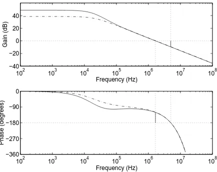
3.2 FREQUENCY RESPONSE . . . .55
3.2.1 Gain Maximization . . . .58
3.3 TIME DOMAIN SIMULATIONS . . . .59
3.3.1 Intermodulation Distortion Reduction . . . .62
3.3.1.1 Effective Amplifier Gain . . . .65
3.3.2 Instability . . . .67
3.4 IMPLEMENTATION. . . .68
3.4.1 Measured Performance . . . .70
3.4.2 Asymmetrical IMD . . . .74
3.5 PRACTICAL CONSIDERATIONS. . . .75
3.6 CONCLUSION. . . .76
4 S
TABILITY ANDN
OISEA
NALYSIS . . . .794.0.1 Summary of stability analysis approach . . . .81
4.1 A PIECEWISE AMPLIFIER MODEL . . . .85
4.1.1 Amplifier model with amplitude non-linearities only . . . .87
4.1.2 Amplifier model with amplitude and phase non-linearities . . . .90
4.2 MIMO MODEL OF CARTESIAN FEEDBACK FOR AMPLIFIERS WITH WEAK NON-LINEARITIES. . . .93
4.2.1 Effects of Amplifier Phase Variations on Stability . . . .93
4.2.2 The Difference between RF Phase Rotation and Baseband Phase Shift . . . .95
4.2.3 Effects of Amplifier Gain Variations on Stability . . . .96
4.3 A GRAPHICAL STABILITY ANALYSIS SUITABLE FOR AMPLIFIERS WITH WEAK NON-LINEARITIES . . . .97
4.3.1 A Universally Applicable Graphical Technique. . . .100
4.3.2 Summary of Amplifier and other Effects on Stability . . . .101
4.4 MIMO MODEL OF CARTESIAN FEEDBACK FOR NON-LINEAR AMPLIFIERS . . . .102
4.4.1 Complex Gain and Perturbations . . . .102
4.4.2 Reduction of Non-linear Amplifier Model . . . .104
4.4.3 MIMO Model of Cartesian Feedback with non-linear amplifiers .109 4.6 A GRAPHICAL STABILITY ANALYSIS SUITABLE FOR NON-LINEAR AMPLIFIERS . . . .112
4.7 TIME DOMAIN SIMULATIONS OF CARTESIAN FEEDBACK WITH NON-LINEAR AMPLIFIERS . . . .117
4.7.1 Spiral Mode. . . .118
4.7.2 Stationary Mode . . . .121
4.7.3 Spiral and Stationary Modes on Graphical Stability Boundaries . .123 4.8 NOISE CONSIDERATIONS . . . .124
4.9 CONCLUSION. . . .130
5 D
YNAMICALLYB
IASEDC
ARTESIANF
EEDBACK . . . .1335.1 HIGH LEVEL MODULATION LINEARIZATION TECHNIQUES. . . .134
5.2 RF DRIVE MODULATION LINEARIZATION TECHNIQUES . . . .136
5.3 DYNAMICALLY BIASED LINEARIZATION . . . .136
5.3.1 Transistor Amplifier Gain Variations with Dynamic Bias . . . .143
5.3.2 Stability and Dynamic Bias . . . .145
5.4 SIMULATION RESULTS . . . .146
5.5 IMPLEMENTATION OF SWITCH MODE POWER SUPPLY. . . .152
5.6 MEASURED PERFORMANCE . . . .153
5.7 CONCLUSION. . . .157
6 C
ONCLUSION . . . .1606.1 CRITIQUE AND FUTURE WORK . . . .164
B
IBLIOGRAPHY . . . .166A
PPENDIXA SMPS D
IFFERENCEE
QUATIONS. . . .173A
PPENDIXB SMPS
S
CHEMATIC . . . .179A
TTACHEDP
APERS1
1 I
NTRODUCTION
Rudimentary communications systems such as telephones and radio have existed for much of the twentieth century. Advances in microelectronics and circuit miniaturization have dramatically transformed these innovations to a point whereby mobile telephony is now commonplace. Rapid developments in mobile and wireless communications will continue to have striking impacts in many areas including commerce, industry, Information Technology (IT), personal communications, and so on.
Extensive and growing use of mobile radio services has however, increased pressures on frequency spectrum allocation. Adopting the cellular architecture has to some extent released the pressure of limited spectrum. In theory, reducing cell sizes could increase capacity to any desired level. In practice however, various factors restrict the minimum cell size. The most prominent of these factors is the high cost of basestation infrastructure.
The push of IT requirements for mobile services to also carry data coupled with the demand for communications systems to interface with the digital system infrastructure, has driven the adoption of new digital modulation techniques in preference to existing analog technologies.
2 Chapter 1
importance since users now expect a compact and lightweight unit which can operate for several hours/days between recharges. The so called “talk-time” of a mobile terminal is often used to attract a larger market share in a highly competitive market. Another significant marketing feature is the improved security aspects of digital communication.
Many recently adopted modulation schemes reflect the constraint that most power efficient forms of RF power amplification are generally non-linear. Techniques based on Continuous Phase Modulation (CPM) which convey information only on the phase of an RF carrier, are generally seen as a good compromise between spectral efficiency and retaining a constant envelope - a necessity with non-linear yet efficient power amplification.
Introducing amplitude variations to the carrier can improve the spectral efficiency allowing higher information throughputs for a given channel. The transmission of these signals however, requires the use of a linear amplifier. This is a serious concern. A linear Class A amplifier operated at the appropriate level of back-off for example, has poor efficiency and would have an excessive deleterious effect on battery life. A non-linear amplifier cannot be used because the distortion of the signal envelope and phase produces intermodulation components in the adjacent channel that cannot be filtered out. Linearizing a non-linear yet efficient RF power amplifier satisfies both requirements of linearity and low power consumption. The aim of this research is to study possible linearization strategies that allow efficient RF power amplifiers (e.g class AB-C) to be used with modern modulation schemes that have a varying envelope.
Efficient linearized amplifiers can be applied in several areas. In mobile communications, applications for linearized power amplifiers can be found in both cellular systems and emerging PMR (Private Land Mobile Radio) systems. In the U.S, the cellular system AMPS (Advanced Mobile Phone Service) has been augmented with DAMPS (Digital AMPS). DAMPS makes use of linear modulation and hence requires linear amplifiers. The move to DAMPS has increased spectral efficiency by three times. Another linearly
3 Chapter 1
modulated cellular system application currently in use in Japan is PDC (Pacific Digital Cellular).
Linear modulation has also been proposed for PMR. Systems such as APCO25 (Ambulance Police Communications Officers) and TETRA (Trans European Trunked Radio) were designed with the availability of linearized power amplifiers in mind. These systems have very tight linearity specifications. Capacity increases and benefits similar to those of digital cellular are expected for these PMR schemes.
Other applications for linearized power amplifiers include NTT Digital Cordless and satellite communication systems such as the Australian OPTUS digital satellite mobile network. It is also possible to apply such amplifiers in traditional systems such as Single Sideband (SSB) High Frequency (HF) radio, and even broadcast Amplitude Modulation (AM) transmitters.
A desirable by-product of linear amplification is the constant gain relationship between input and output of the amplifier. This obviates the needs for output levelling control circuits for transmitters with power control requirements. Power control allows close-by mobiles to transmit at lower powers to those further away (hence reducing the near-far dominated interference at the basestation). This is a major requirement in systems using Code Division Multiple Access (CDMA) such as Qualcomm’s CDMA digital cellular system.
A linear power amplifier is also capable of amplifying signals with any combination of amplitude and phase modulation. This broadens the selection of modulation schemes and increases the versatility of the amplifier considerably. In situations where different modes co-exist on the same band the linearized amplifier is capable of fulfilling the requirements of both modes. The efficient linearized amplifier therefore delivers “a one size fits all” option to manufacturers of mobile equipment. It obviates the need to re-design for new modulation methods when the need arises. Selecting the modulation scheme is simpler
4 Chapter 1
through software control without regard to the RF amplifier. Changing modulation schemes dynamically could have important military applications.
Developments in multicarrier basestations indicate that it is possible to neatly combine individual channels to be transmitted at baseband rather than at high power RF. The traditional RF combination of signals requires the use of several RF power amplifiers, isolators and cavity filters. When the channels are combined at low power, the entire RF band is amplified and fed to a single antenna. The advantages of this technique include reduction in power losses inherent in combiners, isolators and cavity filters, lower overall cost and size, and improved flexibility in terms of channel allocation. The amplifier required for such a design needs to be wideband, highly linear and is consequently a candidate for the application of a linearized RF power amplifier.
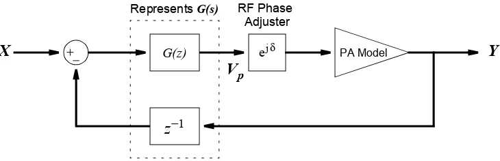
The linearization solutions were developed here by investigating feedback methods which are inherently narrowband. One method - Cartesian Feedback, is a technique of power amplifier linearization using negative feedback of the modulation components. The term cartesian refers to the manner by which the baseband modulation is expressed in its in-phase and quadrature components rather than the polar form of amplitude and in-phase. This linearization technique compares the input modulation signals to those demodulated at the transmitter output and drives the amplifier with the necessary pre-distorted signal such that the output closely matches the input and hence distortion is minimized.
This work extensively covers cartesian feedback and provides a detailed stability and noise analysis. The power efficiency of cartesian feedback was improved by varying the bias conditions of the RF amplifier. This was achieved by careful characterization of the RF amplifier to enable the selection of the best bias conditions for operation at peak efficiency.
Chapter 2 introduces the field of RF amplifier linearization. Much of the early work presented in this thesis concentrated on system characterization. This is dealt with in
5 Chapter 1
chapter 3 where the system was characterized using instruments controlled by GPIB (General Purpose Instrument Bus). The resulting models from the measurements were utilized throughout most of this work. Simulations based on these models are presented in chapter 3 which also discusses the essential details of cartesian feedback linearization and gives results from a constructed system.
Chapter 4 presents an in-depth analysis of cartesian feedback linearization. Both a linear and non-linear piecewise stability analysis are presented along with an out-of-band noise analysis and is the major theoretical contribution to the work.
Chapter 5 describes Dynamically Biased Cartesian Feedback as a means of providing efficiency improvements to conventional cartesian feedback. Simulations are given along with hardware measurements.
The final chapter summarizes the major conclusions of the work presented in this thesis, and the possibility for future work is also discussed.
6
2 BACKGROUND
When communications systems are devised many factors contribute to the overall configuration of the system. One prominent factor is the choice of the modulation scheme. In determining what modulation method will be chosen for digital mobile communications, the system designers generally attempt to meet some specification based on the allowable Bit Error Rate (BER) for given spectrum restrictions. Research into this area has resulted in several techniques being proposed.
Constant envelope modulation schemes are usually adopted if transmitter power efficiency or channel non-linearity is of concern. This was a consideration when Gaussian Minimum Shift Keying (GMSK) was selected for the European and Australian digital cellular system GSM (Global System for Mobile communications). In the digital cordless area, the Digital European Cordless Telephone System (DECT), CT2 (Cordless Telephones), CT3 and the Personal Communications Network (PCN)/Personal Communications Systems (PCS) have adopted (or likely to adopt) constant envelope modulation.
7 Chapter 2
when Nyquist filtering is introduced to digital quadrature modulation. By filtering, the spectrum requirements are reduced at the expense of introducing envelope variations. Linear modulation is overviewed in section 2.1. It will be shown in section 2.2 and 2.3 that such signals when passed through non-linear amplifiers undergo distortion which results in a spreading of the spectrum and a degradation of BER.
Spectral spreading causes interference to other users in the adjacent channels. For this reason authorities specify a maximum adjacent channel interference (ACI) limit; examples are given in section 2.4. To solve the problem of ACI various linearization techniques have been proposed and these are reviewed in section 2.5. One of the more promising techniques is Cartesian Feedback and this is discussed in section 2.6.
2.1 LINEAR TRANSMITTER ARCHITECTURE
Emerging linear modulation schemes are typically transmitted using the direct conversion digital transmitter structure shown in figure 2.1. The Digital Signal Processor (DSP) converts the digital data stream to be transmitted into two baseband analog signals (Iin(t) and Qin(t)). The upconversion process quadrature modulates these baseband signals directly to an RF (Radio Frequency) carrier frequency (ωc). Subsequent linear
amplification brings the modulated RF signal (S(t)) up to a power level suitable for radio transmission.
Figure 2.1: Direct conversion digital linear transmitter.
Quadrature Modulator Linear RF Amplification Digital Signal Processor
D/A D/A
Mapping Σ
90°
PA
Driver(s) Spectral
Shaping
DATA IN
RF OUT LO
cos ωct
Spectral Shaping
Iin(t)
Qin(t)
S(t)
In
Qn
8 Chapter 2
2.1.1 DSP Functions
The DSP circuit first maps the input data stream into two data streams In and Qn where n denotes the nth signalling period or symbol period. The mapping employed will govern what possible discrete values In and Qn adopt and how changes in these values will take place in the next symbol period. If M is used to denote the number of possible states there are generally three types of modulation formats possible: M-ASK (M-level Amplitude Shift Keying), M-PSK (M-level Phase Shift Keying) and M-QAM (M-level Quadrature Amplitude modulation).
Figure 2.2(a) gives and example of 2-ASK otherwise known as on-off keying (OOK). This modulation is generated if all Qn’s are set to zero and the In’s can take a value of either zero or one.
If In = cosΦn and Qn = sinΦn, (where each Φn is taken from M evenly spaced values
between ±π) M-PSK results with each state uniformly distributed on the unit circle. Figure 2.2(b) shows 4-PSK or QPSK (Quadri-Phase Shift Keying), and figure 2.2(c) shows the case for M = 8.
Letting In and Qn take the following possibilities ±1, ±3,..., , generates M-QAM. Figure 2.2(d) demonstrates 16-QAM with the states lying on a square lattice of 16
points. M-QAM can be thought of as a combination of both amplitude modulation (M-ASK) and phase modulation (M-PSK).
Figure 2.2: Scatter diagrams for (a) OOK, (b) QPSK, (c) 8-PSK (or π/4 shift QPSK), (d) 16QAM.
(a) (b) (c) (d)
Qn
In
Qn
In
Qn
In
Qn
In
M–1
( )
±
9 Chapter 2
The scatter diagrams of figure 2.2 give no indication of the nature of movement between different states. Transition between states is governed by the spectral shaping filter and any constraints which the mapping imposes. Figure 2.3 shows the transitions which exist for filtered QPSK and a common mobile modulation scheme π/4 shifted QPSK. For QPSK some of these transitions travel through zero. This ultimately causes the amplitude of the modulated output signal (S(t)) to also cross zero. A zero crossing implies infinite dynamic range and forces operation in typically non-linear turn-on regions of RF PA’s (Power Amplifiers). π/4 shift QPSK was proposed by Akaiwa[1] as a means of avoiding the zero crossing area for linearly modulated digital mobile communications systems1. The “π/4 shift” originates from the fact that the modulation scheme can be generated by rotating (or “shifting”) a QPSK constellation by π/4 radians every alternate symbol. With each symbol (2 bits) a movement is made which is either ±π/4 radians or ±3π/4 radians giving a signal constellation which never passes through zero. The North American DAMPS (Digital-Advanced Mobile Phone Service) system has adopted a differentially encoded version of this modulation, π/4 DQPSK (Differential Encoded π/4 shift QPSK).
Nyquist filtering enables the transmitting of digital information in the smallest possible bandwidth without introducing ISI (Inter-Symbol Interference)[2]. The filtering is an important DSP function and is normally performed in the time domain. One particular form of filter which is currently used extensively and in the DAMPS system is derived from the raised cosine family. By separating the filtering function into two - one at the
1. Under power control however, the turn-on region can still present problems. Figure 2.3: Space diagrams for (a) QPSK, (b) π/4 shift QPSK.
(a) (b)
Qn
In
Qn
In
10 Chapter 2
transmitter and one at the receiver, the filter utilized at each end is a square root raised cosine filter. The frequency response of such a filter is given by [3]
(2.1)
where
f is the frequency,
α is the excess bandwidth, T is the symbol period.
The nature of the filter shows three distinct parts - a flat pass band which continues up to a value determined by the excess bandwidth, a transition band which occupies twice the excess bandwidth, and a stopband which exists outside the excess bandwidth. The excess bandwidth refers to the percentage bandwidth the filter exceeds that of the minimum nyquist filter. The term raised cosine is derived from the transfer function produced when the excess bandwidth is 100% (α = 1) giving a raised cosine function.
The equivalent time domain response is
(2.2)
The impulse and frequency responses described above are shown in figure 2.4 for DAMPS. This figure was generated with the filter design software DFDP2 and shows the
2. DFDP - Digital Filter Design Package, Atlanta Signal Processors Incorporated. B f( ) = 1
B f( )
1 2---πα
è ø
æ ö(2fT–1)
è ø
æ ö
sin –
2
---=
0 f 1+α 2T
---< ---<
1–α
2T
--- f 1+α 2T
---< ---<
f 1+α 2T
--->
B f( ) = 0
b t( ) πsin((1–α)Ωt)+4αΩtcos((1+α)Ωt)
t(π2–16α2Ω2t2)
---= where: Ω 2π
2T ---=
11 Chapter 2
windowed impulse response along with the logarithmic magnitude response. With the DAMPS system α= 0.35 and because the filter impulse response is truncated to a length of 8, a Kaiser window is applied to limit the effects of truncation on the spectral integrity in adjacent channels. The Kaiser co-efficient is 2.4. An oversampling rate of 16 allows the use of a 100kHz reconstruction filter with a data rate of 48.6kBits/s.
The remaining functions in the DSP are the DAC’s (Digital to Analog Convertors) and subsequent reconstruction filters which convert the digitally generated signal to an analog signal ready for modulation.
2.1.2 Quadrature Modulation
The quadrature modulator block shown in figure 2.1 represents a well known technique of directly upconverting baseband analog signals Iin(t) and Qin(t) to a carrier frequency (ωc).
The frequency mixers multiply Iin(t) and Qin(t) with an in-phase and quadrature (+90°) component of a Local Oscillator (LO) respectively. The outputs from the mixers are combined to yield the modulated RF output signal S(t). Since Iin(t) and Qin(t) are modulated orthogonally they effectively occupy two independent I (in-phase) and Q (quadrature) channels.
The quadrature modulation process modulates both the amplitude and phase of a carrier in Figure 2.4: Response of DAMPS filter.
12 Chapter 2
a manner governed by a cartesian to polar conversion, with Iin(t) and Qin(t) being the cartesian representations i.e
(2.3)
It is convenient to consider S(t) as the real part of a complex signal
(2.4)
The complex envelope Sb(t) can therefore be used to describe the RF signal without reference to the carrier signal. A(t) is the amplitude of the signal and Φ(t) is the phase of the signal given by
(2.5)
And the complex envelope signal is given by
(2.6)
Complex baseband envelope representation was used in all of the simulations in this work. This is advantageous since the sample rate does not have to be so high as to accommodate the carrier frequency resulting in higher computational efficiency[4].
2.1.3 Linear RF Amplification
The modulated RF signal S(t) may contain amplitude variations. To amplify such a signal linear RF amplification is needed. Linear Class A RF amplifiers are typically used in driver stages of figure 2.1. This work looks at means by which non-linear (yet efficient) RF power amplifiers can be used in the final stages. The next sections discuss how
non-S t( ) = Iin( )t cosωc( )t +Qin( )t sinωc( )t A t( )[cos(ωc( ) φt + ( )t )]
=
S t( ) Re A t( )e j(ωc( ) φt + ( )t )
[ ]
=
Re A t( )e jφ( )t e jωc( )t
[ ]
=
Re Sb( )t e jωc( )t
[ ]
=
A t( ) = Iin( )t 2+Qin( )t 2 φ( )t QIin( )t
in( )t
---atan =
Sb( )t = Iin( )t +j Qin( )t
A t( )e jφ( )t =
13 Chapter 2
linear amplifiers distort linearly modulated signals and means by which these non-linear amplifiers can be linearized.
2.2 RF POWER AMPLIFIER NON-LINEARITIES
It is common to distinguish large signal amplifiers with class operation set by bias conditions. Most active devices have limited linear regions and bias conditions are normally chosen to give a desired amplifier linearity at the expense of efficiency.
BJT (Bipolar Junction Transistor) amplifiers can be biased to operate under different classes depending on the base-emitter bias voltage (figure 2.5)[5] and corresponding collector currents. Negative voltages push the transistor into operation with lower conduction angles and towards Class C operation. Although lowering the conduction angle improves the collector efficiency3, drive levels must be increased to sustain reasonable output powers. Consequently, power added efficiency4 falls. Finding the optimum bias conditions for maximizing power added efficiency is covered in more detail in chapters 3 and 5.
3. Collector efficiency is defined as Pout/PDC.
4. Power added efficiency is defined as (Pout −Pin)/PDC . 0.7V
ICQ ic
ln(vb)
0.7V
ic
ln(vb)
Saturated Class C Class A
Negative Bias Positive Bias
Saturation
Cut-off
vin vin
iout iout
Figure 2.5: Effect of bias and drive level on class of amplifier operation.
14 Chapter 2
Higher (positive) bias voltages allow the device to operate over more of its linear region thus improving the amplifier linearity. Class A operation occurs when the transistor is biased to conduct for 360° i.e the transistor conducts all the time. This increase in conduction angle however results in lower collector efficiencies.
Increasing the RF drive level leads to a family of amplifiers operating under saturation (e.g saturated Class A, AB, B, C). The transistor begins to behave more like a switch (rather than a current source) giving some gains in power output and efficiency. Indeed, a whole range of switching type RF amplifiers exist (Classes D to F), some with efficiencies approaching 100%[6].
The non-linearities described above are termed AM/AM distortion (Amplitude Modulation to Amplitude Modulation). The deviation from a straight line input-output transfer function in the cut-off region and in the saturation region results in envelope amplitude distortion induced by the amplitude changes on the input. Largely because of voltage dependent collector capacitance (caused by a varying depletion layer width) another form of distortion is introduced, namely - AM/PM (Amplitude Modulation to Phase Modulation). The most disturbing aspect of the AM/PM distortion of the BJT amplifier is the distinct kink when the amplifier leaves cut-off and enters the linear region.
AM/AM and AM/PM distortion is present in most power amplifiers irrespective of the amplifying device. Although much of this research was developed around two BJT RF power amplifiers, TWT (Travelling Wave Tube) amplifiers are commonly used for digital radio and serve as an interesting comparison (figure 2.6). The TWT non-linearity is the analytical model found in SPW5. TWT’s generally have longer delays than BJT’s in addition to the differing characteristics.
This research is mainly concerned with linearization over a relatively narrow frequency
5. SPW Signal Processing Worksystem - The DSP Framework, COMDISCO Systems, Inc.
15 Chapter 2
band. It is common to therefore assume for modelling purposes that the amplifier is wideband compared to the modulation and hence frequency induced variations of the RF amplifier parameters are neglected[7]. Some frequency restriction does however exist in the RF amplifier and this is modelled as an extra delay and discussed in chapter 3. Other frequency dependencies and memory effects can manifest themselves as hysteresis in the time domain. The hysteresis can cause the intermodulation products of a two-tone test to be asymmetrical in the time domain.
2.2.1 Environmental Factors affecting RF power Amplifiers
The characteristics of an amplifier do not remain static. The operating conditions, both internal and external to the amplifying device, will affect the amplifier characteristics. A linearization system must therefore be robust enough to cope with these changes. With feedback systems the control loop robustness is crucial in order to maintain stability.
Thermal time constants within the device and the ambient temperature alter the BJT threshold voltage and peak saturated power capability. Significant memory effects can also be introduced by bias circuitry[8] and power supply variations.
Figure 2.6: Comparison of twt and bjt RF amplifier characteristics. (a) Amplitude response showing AM/ AM distortion. (b) Phase response showing AM/PM distortion.
0 0.2 0.4 0.6 0.8 1
0 1 2 3 4 5 6
twt bjt
Vout (rms volts)
Vin (rms volts)
0 0.2 0.4 0.6 0.8 1
−30 −20 −10 0 10 20 30 40
Vin (rms volts)
Phase (degrees)
bjt twt
vin(rms volts) vin(rms volts)
vout
(r
m
s vo
lts
)
(a) (b)
16 Chapter 2
Another external influence which is especially important with hand portable mobiles is antenna load fluctuations. As the unit is moved towards and away from the head and other objects in close proximity, the changes in standing waves result in a variation of phase angle through the amplifier. Such phase changes will degrade loop stability in feedback systems and can be misinterpreted by some linearization systems as modulation information. Measures such as isolators or other supervisory circuitry are often necessary to overcome these problems. Changes in carrier frequency also result in a phase changes through the amplifier.
2.3 EFFECTS OF NON-LINEARITIES ON MODULATION
Amplifier non-linearities cause distortion of linear signals resulting in two detrimental effects. First, as witnessed by the phase plane diagrams of figure 2.7, the signal trajectories are distorted. Figure 2.7(a) shows the undistorted phase plane trajectory of π/4 shift DQPSK using a root raised cosine filter with a reduced impulse length of two (a reduced impulse length reduces the number of trajectories and makes the figure clearer). After amplification by a non-linear RF PA, the signal trajectories become distorted (figure 2.7(b)). Consequently the received signal will be harder to detect hence degrading the BER[9].
The second effect is that the distortion causes the spectrum to spread into adjacent channels (figure 2.9). Figure 2.8 gives a selection of three complex envelope signals in the time domain with each signal presented in magnitude (amplitude) and phase format. The unfiltered π/4 shift DQPSK modulation is given by figure 2.8(a). Without filtering the envelope will be constant as shown by the upper magnitude trace of figure 2.8(a), and the phase transitions will be instantaneous as shown by the lower trace.
Introducing the full length root raised cosine filter used in DAMPS introduces envelope variations and smooths the phase transitions as shown in figure 2.8(b). After non-linear
17 Chapter 2
Figure 2.7: (a) Undistorted phase plane trajectory of π/4 shift DQPSK using a root raised cosine filter with an impulse length of two. (b) Same signal after amplification by non-linear power amplifier.
(a) (b)
Figure 2.8: Time domain representation in magnitude and phase format. From top to bottom: (a) Unfiltered π/4 Shift DQPSK; (b) Same signal after root raised cosine Nyquist filtering; and (c) Filtered signal after undergoing amplifier distortion.
(a)
(b)
(c)
Figure 2.9: (a) Unfiltered π/4 Shift DQPSK. (b) Same signal after root raised cosine Nyquist filtering. (c) Filtered signal after undergoing amplifier distortion.
(a) (b) (c)
18 Chapter 2
amplification the AM/AM distortion corrupts the envelope and the AM/PM distortion corrupts the phase (figure 2.8(c)).
Figure 2.9 shows the spectrum of the same three signals. Figure 2.9(a) is the original unfiltered π/4 shift DQPSK signal. After the application of the nyquist filter, the bandwidth required to transmit the data is substantially reduced (figure 2.9(b)). Non-linear amplification however degrades the spectrum, spreading it back into the adjacent channels and hence destroying the benefits of the nyquist filtering.
2.3.1 Intermodulation Distortion Measurement
Intermodulation distortion is generated by amplifier non-linearities. Linearization aims to remove these non-linearities and hence remove the intermodulation distortion artifacts which interfere with adjacent channels. The two-tone test is a common method used to quantify the degree of non-linearity in an amplifier (or other non-linear devices such as mixers).
The test involves generating two tones at the carrier frequency as shown by the solid lines of figure 2.10. This is easily achieved where quadrature inputs are available since applying a single tone (with frequency fm) at either the In-phase or Quadrature input will yield two tones at RF. With RF inputs, two RF signal generators can be combined. After passing through the non-linearity the two tones intermodulate resulting in the undesired products as shown by the dashed lines in figure 2.10 (fc ± 3fm, fc ± 5fm etc.). The amplitude of the distortion products relative to the desired tones is a measure of the amplifier non-linearity.
Distortion also occurs at a carrier rate which results in harmonics being generated at multiples of the carrier frequency (i.e 2fc, 3fc etc.). These are normally removed by a harmonic filter in which case the harmonics can be neglected. A frequency product is also generated at 2fm as a result of the presence of distortion around even order harmonics at
19 Chapter 2
2fc, 4fc etc. This product is also neglected due to the high-pass nature of the amplifier output. Occasionally even order distortion is also visible in measured two-tone tests at fc and even order intervals (fc ± 2fm, fc ± 4fm etc.). This distortion is caused by asymmetry, DC or carrier leak.
A related method used to quantify non-linearity is the third order intercept point. The intercept point graph (see figure 2.13a) is generated by performing a series of two-tone tests at different power levels. Idealized slopes of the fundamental output power (1:1 slope on a dB scale) and of the third order products (3:1 slope on a dB scale) are taken well before compression and extended right up to form an intercept point. The higher this point with respect to the operating point the more linear is the system. The intercept point approach is applicable for weak non-linearities, however some of this work deals with strong non-linearities and hence the raw two-tone test is used to assess the performance of linearization schemes.
2.4 ACI RESTRICTIONS
The usual cause of ACI is distortion in the amplification system but other causes exist, such as leakage from the Nyquist filter in the modulation. The situation shown in figure
fc − fm
2fc +2fm
fc +3fm fc − 3fm
fc + 5fm fc − 5fm
Figure 2.10: Distortion products generated by two-tone test passing through a non-linearity; dashed box indicates zone normally viewed on spectrum analyzer. Desired signals solid, undesired distortion products dashed.
fc
2fm 2fc
3fc − fm
fc + fm
3fc +3fm
3fc − 3fm
3fc + 5fm
3fc − 5fm
2fc +2fm
2fc +4fm
2fc +4fm
3fc + fm
2fc 3fc
DC
20 Chapter 2
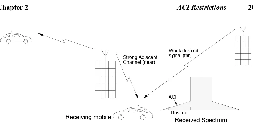
2.11 demonstrates the near-far problem as it relates to ACI. The problem occurs when the receiver attempts to receive a weak signal (i.e far) in the presence of a strong (i.e near) adjacent channel transmission. If the ACI specification in the transmitter is too high the weak signal will be swamped.
The level of ACI is a specification set in all mobile communication applications and some examples are given in the next few sections.
2.4.1 Cellular Systems
The most immediate application for linearized power amplifiers is DAMPS. The level of ACI in the adjacent channel is −26dB and in the next adjacent channel −45dB. In other channels the ACI specification is given as −60dB. Cellular systems are able to modify frequency allocations in order to eliminate most of the near-far conditions. Although the specification seems lax, some of the ACI specification has been used up by the modulation scheme adopted and so intermodulation requirements are still quite tight.
2.4.2 Mobile Satellite
Unlike cellular systems the near-far effect does not exist with satellite systems since all Figure 2.11: Near-far problem in a mobile communications scenario where ACI from a strong (near) adjacent channel interferes with a weak (far) desired signal.
Desired ACI
Weak desired Strong Adjacent
Channel (near)
signal (far)
Received Spectrum Receiving mobile
21 Chapter 2
the mobiles are operated at long distances. However some operators allow users to access the satellite at different power levels which produces a pseudo near-far problem. Consequently systems such as Australian Optus Mobilesat can set ACI at −35dB in the adjacent channel and −50dB for all other channels.
2.4.3 Private Land Mobile Radio (PMR)
Most PMR systems presently in use utilize analog FM as the modulation system. As with mobile cellular there is a trend towards digital transmission which can relay data (for despatch purposes etc.) and voice. A new digital modulation system would have to co-exist with current analog users for quite some time. The scattered and uncontrolled nature of PMR basestations causes severe near-far problems and hence the ACI specification is quite tight e.g −70dB for APCO25 and −60dB for TETRA.
2.4.4 Future Systems
It is likely CDMA systems will feature prominently in future communications systems. Qualcomm's proposed CDMA cellular and mobile satellite systems for example, will require some linear amplification and wide dynamic range power control. Power control is crucial in CDMA systems and hence any linearization strategy should consider this additional requirement.
2.5 REVIEW OF AMPLIFIER LINEARIZATION TECHNIQUES
Varying degrees of distortion is always present in electronic systems. Early work in amplifier linearization focused on cross-modulation distortion present in multichannel systems and on intermodulation distortion of amplitude modulated signals. Although the linearization techniques developed here were aimed at mobile radio, much of the linearization work reviewed spans many applications including: fixed point-to-point microwave radio links, CATV (Community Antenna Television), satellite
22 Chapter 2
communications and multi-carrier basestations. In each case the objective is to improve linearity without sacrificing efficiency.
Despite the broadness of the linearization area, the linearization techniques can be roughly divided into a number of approaches - some of which draw from similar roots. Figure 2.11 shows graphically how the various linearization techniques interrelate.
2.5.1 Back-off of Class A
Amplifier back-off is the conventional approach of improving RF power amplifier linearity. The technique involves operating power amplifiers at a fraction of their saturated output power potential. The further the device is “backed-off” the better the improvement in intermodulation distortion. A 1dB back-off or reduction in output power (i.e a 1dB reduction in the fundamental frequency output power) results in a 3dB reduction in the 3rd order intermodulation distortion, a 5dB reduction in the 5th order intermodulation product and so on. This results in a 2dB, 4dB etc. improvement respectively (figure 2.12a). Since the DC power dissipation remains constant irrespective of the output power for a class A amplifier, the efficiency of the amplifier diminishes as linearity improves. Consequently to achieve the intermodulation performance desired for
LINEARIZATION
BACK-OFF OF CLASS A
FEEDFORWARD VECTOR-SUMMATION PREDISTORTION FEEDBACK
RF BASEBAND BASEBAND RF IF LINC LIST
ADAPTIVE DSP POLAR CARTESIAN CALLUM
DYNAMICALLY BIASED MULTI-LOOP
Figure 2.12: Amplifier linearization techniques
DYNAMICALLY BIASED CLASS A
AUTOMATICALLY SUPERVISED
EER
23 Chapter 2
most mobile communication applications the amplifier will be unduly wasting significant amounts of DC power (figure 2.12b). For many mobile applications the efficiency will be below 1%. Such a condition is highly undesirable in portable wireless applications. Further disadvantages are also incurred since the size of devices tend to be larger and thus heavier, and usually are more costly.
2.5.2 Dynamically biased Class A
This technique was introduced by Saleh[10] as a means by which the power-added efficiency of Class A Field Effect Transistor (FET) could be improved when operating with linear modulated signals. Instead of fixing the gate bias of an FET to roughly midway between the pinch off voltage (Vp) and zero volts (the condition for Class A operation), the gate bias voltage (Vg) is varied dynamically in response to the envelope of the input signal given by Ve(t), such that Vg = −Vp + Ve(t). This way the FET is nearly turned off when Ve(t) approaches its minimum and the mean gate bias voltage is just enough to ensure the FET has sufficient dynamic range for the input signal. The benefits Figure 2.13: (a) Fundamental output power (solid) and third order intermodulation distortion (dash-dot) versus input power for a two-tone test. Fundamental power rises on a one-to-one basis whereas third order power rises on a three-to-one basis (dB scale). Interception of both gradients is shown with an asterisk. (b) Power added efficiency (ηadd) versus input power under the same conditions as (a).
−250 −20 −15 −10 −5 0 5 10
1 2 3 4 5 6 7 8 9 10 Pin (dBm) add (%)
−25 −20 −15 −10 −5 0 5 10 15
−50 −40 −30 −20 −10 0 10 20 30 40 50 Pin (dBm) Pout (dBm)
3rd Order Intercept Point
1
1
3
1
(a) (b)
Pin(dBm) Pin(dBm)
ηadd (% ) Pout (d B m )
24 Chapter 2
of such a biasing scheme include higher power added efficiency at microwave frequencies.
2.5.3 Feedforward Linearization
Feedforward was invented as means of distortion reduction in amplifiers by Black[11]. This technique is usually applied directly at RF and is shown in figure 2.13.
The feedforward scheme consists of two sections. The first compares an attenuated version of the power amplifier (PA) output with the PA input to get the distortion generated in the PA. This distortion (given by “Error” in the diagram) is destructively combined at the output of the PA by a linear auxiliary amplifier. The resultant output is then ideally distortion free. The process has been demonstrated in the diagram for a two-tone test input. The two time delays are necessary to match any delay and frequency dependent phase shifts introduced by the respective amplifiers. Any deviation from exact amplitude and phase matching will degrade the subtraction process and subsequent distortion cancellation[12].
Amplitude and phase matching is a problem since amplifier characteristics tend to drift with temperature and time, and also vary with manufacturing tolerances. Adaptive
τ2
Error Subtractor
Time delay Auxiliary
Amplifier
Combiner Power
Amplifier Coupler Time delay
τ1 Input
Coupler
RFin RFout
Figure 2.14: Feedforward linearizer implemented at RF. PA
25 Chapter 2
techniques enable the performance of the system to be maintained despite these effects[12-13].
Efficiency of the feedforward system is reduced by the power consumption of the auxiliary amplifier which must be linear and have a high enough output power capability to overcome the loss through the output coupler.
Feedforward linearization can however deliver reasonable linearization performance (20dB-40dB improvement) over relatively wide bandwidths (3MHz-50MHz) and has the advantage of inherent stabilty[14-15].
2.5.4 Vector Summation
Vector Summation[16] is a technique which exploits the fact that the combination of two or more constant envelope signals can result in a signal with a varying envelope and phase. This arbitrary amplitude and phase modulation can be obtained by selecting the appropriate phase relationship of each of the constant envelope carriers. Amplification of constant envelope signals need not be linear and hence the use of highly efficient amplifiers is possible. The main disadvantage is the inherently lossy nature of the combining process which reduces the overall efficiency.
2.5.4.1 LINC
Component Separator
PA
PA
Σ
1 1
1.25 S(t)
S1(t) S2(t)
g
g
gS(t) S1(t)
S2(t)
S(t)
gS2(t)
gS2(t)
Figure 2.15: (a) Block diagram of LINC transmitter. (b) The combination of two constant envelope vectors (S1(t) & S2(t) yields a replica (S(t)) of the desired output signal (gS(t)).
(a) (b)
26 Chapter 2
LInear amplification with Non-linear Components (LINC)[17] is a special case of vector summation. It uses two constant envelope signals to obtain the desired output signal (figure 2.14). The component separator uses analog or DSP techniques to generate the constant envelope signals (S1(t) and S2(t)) such that when amplified and then combined these signals produce the desired output signal (gS(t))[17-20].
With conventional combining techniques an average combining loss of 3dB occurs reducing the maximum possible efficiency of LINC to 50%. Overall efficiencies of 21% are easily achievable[18].
The LINC technique is susceptible to amplitude and phase differences in each of the paths. Differences in these paths can severely degrade system performance [18-19] and some form of feedback is usually necessary in order to compensate for variations in the amplifiers [18, 21].
2.5.4.2 CALLUM
The Combined Analogue Locked Loop Universal Modulator (CALLUM) proposed by Bateman[21] cleverly overcomes the complexity of DSP circuits whilst simultaneously coping with amplitude and phase differences in the two paths. The technique (figure 2.15) uses two feedback loops and VCO’s (Voltage Controlled Oscillators) to generate the correct constant envelope signals. Under stable operation, the VCO’s automatically take
VCO VCO
PA
Σ
gg
gS(t) S1(t)
S2(t)
Iin(t) gS2(t)
gS2(t)
Qin(t)
90°
Figure 2.16: The Combined Analogue Locked Loop Universal Modulator (CALLUM) transmitter. LO
PA
27 Chapter 2
up the frequency of the Local Oscillator (LO) and therefore preform frequency translation. Furthermore the VCO's are driven to generate the necessary constant envelope LINC signals (S1(t) & S2(t)) and if these oscillators are power types, they could also provide the RF power given by the RF power amplifiers in conventional LINC systems.
Bateman demonstrated 55dB of intermodulation distortion suppression was possible for a Nyquist filtered (α = 0.3) OQPSK (Offset QPSK) with a bandwidth of 30kHz. The CALLUM system does however rely on feedback which implies the potential for instability and errors introduced by the feedback gathering components (mainly in down converting mixers). Stability and further aspects of CALLUM are discussed in [22].
2.5.4.3 LIST
LInear amplification by Sampling Techniques (LIST)[23] is demonstrated in figure 2.16. The technique is similar to LINC in that it utilizes two constant envelope signals which are combined at the output to derive the desired linearly amplified output. The main difference to LINC is that the two signals can each only take two discrete phase values and are in effect combined in quadrature. The quadrature arrangement of the two constant envelope signals effectively gives four possible phase outputs.
Iin(t)
Qin(t)
gS(t)
D Q
D Q
PA g
g
Σ
90° LO
CLOCK
Delta Coder
Delta Coder
Figure 2.17: Linear amplification by Sampling Techniques (LIST) transmitter. PA
28 Chapter 2
The delta modulators shown in the dashed boxes enable any of the four possible phases to be selected in rapid secession at a rate given by the clock frequency. Filtering at the output reconstructs the signal to give the smoothed desired linearly amplified signal.
Cox[23] demonstrated that intermodulation products 40dB below the desired signals for a two-tone test (100kHz between tones) was possible for an amplifier operating at 70MHz.
The advantage with the technique is the relative ease by which the two constant envelope signals can be generated. Feedback was also proposed in [23] giving a similar improved tolerance to amplifier differences as with CALLUM. Delay in the delta coders and filtering components however reduces the amount of feedback that can practically be applied
2.5.5 Predistortion
Predistortion is a technique which modifies the input to a power amplifier such that it is complementary to the distortion characteristics of the amplifier (figure 2.17a). The cascaded response of complementary predistortion and amplifier distortion should therefore result in a linear response (figure 2.17b). The technique is generally applied at RF, IF or baseband.
2.5.5.1 RF Predistortion
Synthesizing an exact complement of an RF power amplifier at radio frequencies can be difficult. Usually an attempt is made to reduce the third order intermodulation products only by use of a cubic type canceller[24-28]. A block diagram of a cuber predistorter is
Figure 2.18: (a) Combination of complementary predistortion and amplifier distortion yields (b) linear transfer.
(b) (a)
29 Chapter 2
shown in figure 2.18.
A cubic law device (x3 in the diagram) is used to generate third order distortion based on the magnitude of the RF input. This (pre)distortion is then added to a delayed version of the input and applied to the non-linear RF power amplifier. The amplitude and phase shift of the third order distortion is manipulated such that the third order distortion generated within the amplifier is cancelled. Making the adjustment adaptive can allow this technique to track drifts in the amplifier characteristics[24-25].
The cubic law device can be realized in a number of ways. Usually diodes are used with either a quadrature hybrid[25-26] or a circulator[27]. Alternatively a compressed amplifier[28] can be used.
The scheme is only suitable for weakly non-linear amplifiers since only third order distortion products are cancelled. Implementation at RF does however allow wide-band operation. Nojima[25] for example reported more than 20dB improvement in intermodulation distortion over a 25MHz bandwidth at 800MHz. Occasionally the predistortion is applied at an Intermediate Frequency (IF) to enable easier implementation for higher frequencies[29]. The potential disadvantage with IF techniques is the possible degradation introduced by the up conversion process.
There are other RF predistortion techniques and some will only be mentioned here. These
x3
Delay
Atten. Phase
PA
RFin RFout
Figure 2.19: Cubic canceller predistortion system.
Σ
30 Chapter 2
include: techniques aimed at suppressing AM/PM distortion using varactor diodes or ferrimagnetic materials[30]; and techniques which attempt to synthesize RF predistortion using circuits such as: RF driver stages whose distortion complements that of the main power amplifier; or transistor circuits which have non-linear elements in various feedback arrangements[31]. A more elaborate polynomial analog predistorter using mixers has also been proposed[32].
2.5.5.2 Baseband Predistortion Using DSP
Digital Signal Processing (DSP) offers the possibility of synthesizing complex predistortion characteristics. Because of speed limitations the predistortion must be applied at baseband and subsequently up converted. The linearization bandwidth is hence generally limited due to DSP processing. A generic DSP predistorter is shown in figure 2.19.
The forward path takes the digitized modulation signal and predistorts it in a complimentary manner to the amplifier distortion. The digital output is then converted into an analog signal for upconvertion and subsequent amplification by the non-linear RF amplifier. The upconversion process is typically performed with a quadrature modulator, however IF upconversion is possible. Optional adaptation feedback can be used to track out drifts in the amplifier and to also find the predistortion needed to achieve linear amplification.
D/A
A/D
Predistort PA
Up-Convert
Down-Convert
Figure 2.20: Generic block diagram representation of an adaptive baseband DSP predistortion linearizer. Digital
Input
31 Chapter 2
The actual predistortion can be accomplished using polynomial representation, or with input output look up tables. Polynomial representation is the baseband equivalent[33] of the cuber predistorter described above. Since DSP offers more computational capabilities, higher order polynomials are possible resulting in a better representation of the desired predistortion. The main disadvantage with polynomial representation is the relative difficulty in having stable and effective adaptation algorithms.
The look up table predistorter is more popular for DSP implementation. The predistortion tables can take different forms. The most straightforward is the polar complex gain form shown in figure 2.20(a). This predistorter consists of two one dimensional tables. The amplitude map predistorts for the amplifier’s AM/AM distortion and the phase map predistorts for the AM/PM distortion. The address of both maps is driven by the amplitude of the input signal. Faulkner[34] presented an adaptive polar predistorter using this technique. Interpolation between points in the tables allowed the use of a relatively small table size with only 64 entries. The computational effort necessary for the polar to rectangular conversion was found to be a potential problem. The overall computational load was quite high and with an ordinary DSP (TMS320C25) intermodulation distortion was reduced by 30dB over a limited 2kHz bandwidth. Another polar mapping predistorter proposed the use of cubic spline interpolation[35].
Cartesian complex gain tables avoid polar conversions and require a lower DSP processing load (figure 2.20b). Cavers[39] proposed the use of cartesian tables addressed by the signal power. Complex multiplication by the input signal is then used to apply the
Figure 2.21: Three examples of table based predistortion (a) Polar complex gain, (b) Cartesian complex gain, and (c) Full cartesian mapping.
(a) (b) (c)
Cartesian to Polar
AM/AM AM/PM
Polar to Cartesian
I Q I Q
Address
Address 2d Address
Iin Qin
Iout Qout
Iin
2
Qin
2 +
Iin Qin
Iout Qout
Iin Qin
Iout Qout
Complex Multiply