A NOVEL TECHNIQUE FOR IMPROVING THE PERFORMANCE OF SALISBURY SCREEN A. A. Abdelaziz
Faculty of Engineering
Misr International University (MIU) Cairo, Egypt
Abstract—The most common and simple structure to reduce the level of the reflected power from a metallic surface is the single layer structure known as Salisbury screen which is a sheet of porous material impregnated with graphite and spaced a quarter-wavelength off a metallic backing plate. The main disadvantage of this mechanism is the narrow frequency bandwidth. Many techniques have been reported to improve the working frequency bandwidth but with some degradation in the other technical properties of the overall structure. In this paper a novel technique has been introduced based on a spatial kind of material called circuit analog screen. Theoretical analysis shows that the bandwidth of the reflected power will be improved if the graphite sheet of Salisbury screen has been loaded by circuit analog screen with spatial geometry with spatial parameters.
1. INTRODUCTION
for impedance of periodic arrays of thin continuous conducting strips. The theoretical results of the novel technique show that the working bandwidth of the reflected waves has been improved more than twice of the old one without any degradation of the original performance.
2. NORMAL INCIDENCE SCATTERING FROM FLAT DIELECTRIC MULTILAYER
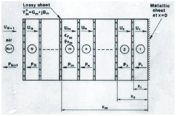
Calculation of the reflected power of a normally incident plane wave from an infinite flat multilayer structure is a straightforward problem involving application of boundary conditions derived from Maxwell’s equations to the general solution for the electric and magnetic fields in each layer. The basic structure consists of a finite number of dielectric layers stacked against a metallic backing plate as shown in Figure 1. Calculation of reflected power in dB of normally incident plane wave form layers is given by:
|R|= 20 log10Pm
Um
(1)
whereUm,Pmare the amplitudes of forward and backward propagation waves and equal to (2):
Um = e
−jkmxn
2Ym
[Un(Ym+Yn+Yms)ejkmxn+Pn(Ym−Yn+Ys
m)e−jkmxn]
Pm = e
jkmxn
2Ym
[Un(Ym−Yn−Yms)ejkmxn+Pn(Ym+Yn−Ys
m)e−jkmxn] (2)
wherem=n+ 1;
Ym is the normalized, toY0, layer intrinsic admittance and is given by:
Ym =
ε
rm
µrm
.
Y0 is the free space admittance equal to 1/377 Ω.
Yms is the normalized, to Y0, sheet admittance and given by: Yms = Gm+jBm.
3. SINGLE LAYER WITH CONDITION OF MINIMUM REFLECTED POWER
Consider only one covered dielectric layer, see Figure 1, withεr=µr =
1 and k2 =k1 = k0, free space wave number, then Equation (2) will be:
U2 =
e−jk0x1
2 {[2 + (G1+jB1)]e
jk0x1 −(G
P2 =
ejk0x1
2 {−(G1+jB1)e
jk0x1−[2−(G
1+jB1)e−jk0x1]} (3)
where P1 =−U1 for a metallic backing atx= 0.
Figure 1. Configuration of multi-covered layer.
From Equations (1) and (3), the reflected power will be minimum ifP2 is forced to be zero, andP2 will be zero ifG1 = 1 andB1 satisfies the following condition: 0 =−(1 +jB1)ejk0x1−(1−jB1)e−jk0x1, after some manipulations:
B1 = cot(k0x1) (4)
Equation (4) gives the value of susceptance B1 of the loaded lossy sheet for minimum reflected power and is plotted as shown in Figure 4(a), the dotted curve, for separation distance x1 = 7.5 mm and frequencies from 1 up to 18 GHz.
4. INVESTIGATION OF A CIRCUIT ANALOG SCREEN WHICH SATISFIES THE CONDITION OF MINIMUM REFLECTED POWER
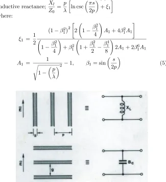
pattern controls the effective inductance and capacitance. Thus, the layer can be tailored to specific values of inductance and capacitance and its performance can be analyzed in terms of lumped elements. An infinitely extended plane grating, shown in Figure 2, formed by metallic strips of zero thickness with edges parallel or perpendicular to the electric field E and with normal-wave incidence has been analyzed by Marcuvitz [5]. The equivalent circuit’s parameters, normalized values, are frequency dependent and are equal to [5]:
Inductive reactance; Xl
Z0 = p λ ln csc πs 2p +ξ1
where:
ξ1 = 1 2
1−β12 2
2
1−β
2 1 4
A1+ 4β12A1
1− β
2 1 4
+β12
1 +β
2 1 2 −
β14
8
2A1+ 2β61A1
A1 =
1 1− p λ
2 −1, β1= sin
s
2p
(5)
And;
Capacitive susceptance; Bc
Y0 = 4p
λ ln csc πg 2p +ξ2
where:
ξ2 = 1 2
1−β22 2
2
1−β
2 2 4
A1+ 4β22A2
1− β
2 2 4
+β22
1 +β
2 2 2 −
β24
8
2A2+ 2β62A2
A2 =
1 1− p λ
2 −1, β2= sin
πg
2p
(6)
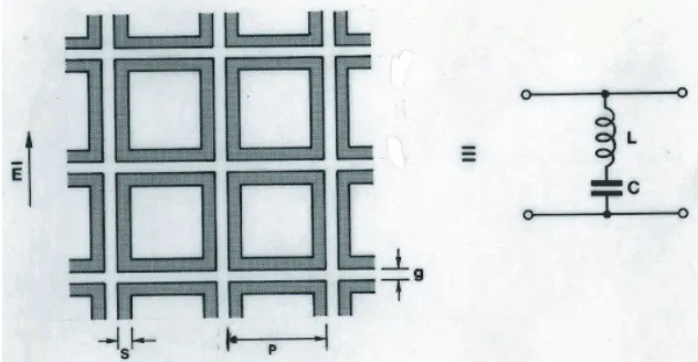
The easiest way to represent the inductive-capacitive circuit equivalent to what is given by Equation (4) is to consider the square loop array as shown in Figure 3 which consists of the metal strips given in Figure 2. An Array of square-loops has been modeled [6, 7] based on equations given by Marcuvitz [5]. The equivalent circuit model of square-loop array is represented by a single series LC circuit shunted a transmission line. A computer program has been written to calculate the normalized values of a shunt inductive reactance (Xl)
and capacitive susceptance (Bc) given by equations (5, 6) for different values ofs,gand p shown in Figure 3. The solid curve in Figure 4(b)
shows the computed results of susceptance B of a lossless square-loop array with valuess= 2, g= 2, and p= 12 mm and frequency from 1 up to 18 GHz. The results are very near to that required from condition of minimum reflected power given by Equation (4).
5. CALCULATION OF THE REFLECTED POWER
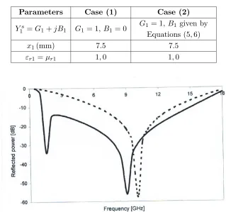
To calculate the reflected power from a single layer, see configuration given in Figure 1, for two different cases given as:
Case (1): Single layer covered with only resistive sheet.
Case (2): Single layer with a cover consists of a resistive sheet loaded by the square-loop array shown in Figure 3.
A computer program has been written based on Equations (1, 2) to calculate the reflected power in dB with the parameters given in Table 1.
Figure 4. Susceptance (B) versus frequency for two different cases: (a) - - - Condition for minimum reflected power given by Equation (4), (b) —— Square loop array shown in Figure 3 with
s= 2, g= 2, andp= 1.
The computed results are shown in Figure 5. The dotted curve for the case of resistive sheet only and has a minimum reflected power ∼
Table 1. The parameters of single layer for the configuration of Figure 1.
Parameters Case (1) Case (2) Ys
1 =G1+jB1 G1= 1, B1 = 0
G1 = 1,B1 given by Equations (5, 6)
x1(mm) 7.5 7.5
εr1 =µr1 1, 0 1, 0
Figure 5. Reflected power from single layer, configuration of Figure 1, for two different cases: (a) - - - Only resistive sheet with G1 = 1, B1= 0, (b) —— Resistive sheet loaded by square loop array shown in Figure 3.
6. CONCLUSION
The new structure of Salisbury screen which is loaded by circuit analog screen has been analyzed to find out the optimum condition for minimum reflected power in terms of the susceptance of the loaded sheet. A square loop array sprayed on thin plastic sheet has been used as an equivalent to the susceptance investigated for minimum reflected power. The calculated results of the reflected power from the novel technique show an improvement in the working bandwidth of the reduced reflected power of Salisbury device more than twice without any penalties in the weight or thickness.
REFERENCES
1. Salisbury, W. W., “Absorbed body of electronic waves,” U.S. Patent No. 2, 599, 944, June 10, 1952.
2. Gustafsson, M., “RCS reduction of integrated antenna arrays with resistive sheets,”Journal of Elec. Waves and Application, Vol. 20, No. 1, 27–40, 2006.
3. Knott, E. F., J. F. Shaeffer, and M. T. Tuley,Radar Cross Section, Artech House, London, 1993.
4. Henderson, A., A. A. Abdelaziz, and J. R. James, “Investigation of interference suppression radome for microstrip arrays,”Proceeding ICAP, Edinburgh, 1993.
5. Marcuvitz, N., Waveguide Handbook, Peter Peregrinus Ltd., London, 1986.
6. Langley, R. J. and E. A. Parker, “Equivalent circuit of square loops,”Electronic Letters, Vol. 18, No. 7, April 1982.