Automatic Power Theft Locator
Isizoh A. N.P
1
P
Asogwa T.C.P
2
P
Okide S. O.P
3
P
Nwobodo H. N..P
4
P
1
P
Dept. of Electronic and Computer Engineering, Nnamdi Azikiwe University, Awka, Nigeria. E-mail:
P
2,4
P
Dept. of Computer Engineering,Enugu State University of Sci. and Tech.,Enugu, Nigeria.
P
3
P
Dept. of Computer Engineering, NnamdiAzikiwe University, Awka, Nigeria.
Abstract
This paper presents the design and analysis of a power theft location system which alerts a Power company in the event of theft or attempted theft of electrical energy. The system utilizes an electro-optical sensor incorporated into an energy meter to detect when the meter cover is opened. This triggers a series of actions within the system which eventually lead to the sending of a message containing the meter number and address from which the tampering originates to a computer which will be located at the Power Company’soffice. This paper discusses in detail the steps undergone in realizing the work including the design calculations, implementation and testing. The design was made with reliable and readily available components in the market. The system was tested and the operations were found satisfactory.
Keywords: Microcontroller, phone, comparator, transformation, flowchart, modem.
Introduction
With the advancement of technology, particularly in the field of microcontrollers, all the activities in our day to day living have become a part of information and we find microcontrollers at each and every application. Nowadays, energy distribution/consumption has become a big subject for discussion because of huge energy theft. Theft in this case refers to a deliberate attempt to steal considerable amount of energy by ensuring no/low energy recording in the metering device. Hence, there is a need to think in this line and proffer a solution to this ugly trend. Thus this paperfocuses on electrical energy monitoring so that energy theft can easily be detected and huge penalties be imposed on
these thieves. By detecting energy theft cases, the economy of a nation can grow rapidly.
This research paper is aimed at developing a system which monitors and detects incidences of power theft, whether in the form of connecting load directly to the power line or bypassing the energy meter thereby paying less than what is consumed or by changing connection of lines. The type of microcontroller used for this monitoring and detection is AT89C52 microcontroller.
Objectives of the Paper
The objectives of thisresearch paper are: (i) to provide a vivid understanding of microcontroller as well as its interfacing to other input/output devices (ii) to detect the theft of electrical energy (iii) to prevent the illegal use of electrical power (iv) to reduce the pilferage of energy to a considerable extent.
In order to achieve the above set objectives, this paper is categorized into two sections namely: Energy theft detection unit (transmitter section) which is located at the consumer’s place anda centralized display unit, using GSM phone (receiver section) located and monitored continuously at the energy distribution area.
The paper is limited to two representations (models) involving (i) electrical energy meter with a sensor as a detecting device which is connected to a controller sub-circuit and a GSM phone that establishes a link between the consumer’s residence and the Power distribution station, all placed inside the meters (ii)a computer that displays the meter number at thePower distribution station whenever there is a power theft. The basic instruction set of the AT89C52 microcontroller was used to develop a
control program written in Assembly language, and this program enables the microcontroller to provide a vital link with other devices so as to control allthe activities within the system [1].
Methodology
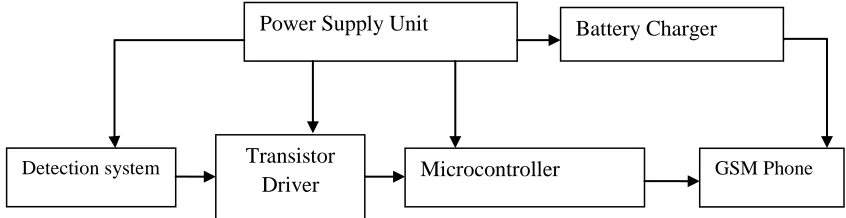
The system was designed using many devices and later programmed. These devices are arranged as modules in the block diagram shown in figure 1.
U
Power Supply Unit
The design of every power supply unit is of paramount importance. It happens to be the basic building block of every electronic design in the sense that the overall functionality of the design depends on it [2]. The required voltage of the system is supplied by the power supply. Every electronic circuit requires a Direct Current (DC) voltage as against the Alternating Current (AC) voltage supplied by electricity Distribution Company. This AC voltage is usually stepped
down andthen converted to the required DC level source so as to power the sub-circuits. In order to achieve this required DC for this system, the following are required: a 240/12Vtransformer, bridge rectifier, filtering capacitor, and a voltage regulator. The interconnections of the above components give rise to the power supply unit. The block diagram is shown in figure 2.
U
Transformation
Transformer is always used for transformation. The transformer consists of two closely coupled coils (primary and secondary coils). The function of the transformer is to stepdown the voltage from 240V to 12V. To achieve this transformation, the relationship between the primary and the secondary windings is given as:
𝑁𝑝
𝑁𝑠 =
𝐸𝑝
𝐸𝑠 =
𝐼𝑠
𝐼𝑝… … … . .1
Where:
NRpR is the number of turns in the primary coil
NRsR is the number of turns in the secondary coil
ERpR is the primary voltage or EMF
ERsR is the secondary voltage or EMF
IRpR is the primary current
IRsR is the secondary current
For a primary input voltage of 240V and a required secondary output voltage of about 12V, the turns ratio required is thus:
Power Supply Unit
Microcontroller GSM Phone
Detection system
Fig. 1: Block diagram of the entire system Transistor
Driver
Battery Charger
AC input
Transformation Rectification Filtering
Voltage
Regulation
DC output
Fig. 2: Block diagram of the power supply unit
Np Ns=
240 12 =
20
1 ………2
Therefore the turns ratio of the primary to the secondary is given as 20:1. However, due to the voltage drop encountered across the diodes during the rectification process, such transformers are not designed to produce exactly 12V at their secondary windings. This is done so that with the regardless of the losses, the voltage produced for utilization is still sufficient [3]. Suppose the voltage required at the input of the regulator is 12V, we add 10% of this value to take care of the ripple voltage, and then add the voltage drop across the two diodes of the rectifier (since only two of the four diodes of the rectifier are conducting at any time). The ripple voltage is the difference between the peak voltage and the minimum voltage provided by a supply. The voltage drop across a silicon diode is 0.6V. So the voltage at the secondary winding would be
12𝑉+ 1.2𝑉+ (2∗0.6)𝑉 = 14.4𝑉………..3
The transformer used for this analysis is a 240/12V, 500mA. The 500mA implies that the maximum current that can flow in the entire circuit is 500mA.
U
Rectification
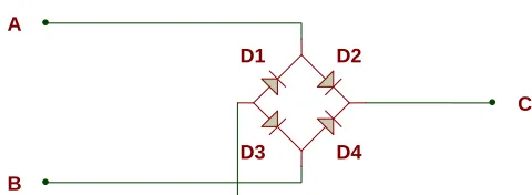
Bridge rectifier was used for rectification. A bridge rectifier is a device that converts alternating current (AC) to direct current (DC). The process of rectification is brought about by the use of two or more diodes. Rectifier can be half-wave, full wave or bridge rectifier. Half wave rectification is achieved using only one diode while full-wave is achieved using two diodes. The type of rectifier required for this work is bridge rectifier and it is achieved by connecting four diodes in a manner shown in figure 3 below.
The alternating current is fed to the bridge rectifier through terminals A and B while the rectified direct current is tapped from terminals C and D. During the positive half cycle, DR2R and
DR3R are forward-biased while DR1R and DR4R are
reverse-biased. During the negative half cycle, DR1R and DR4R become forward-biased while DR2R and
DR3R are reverse-biased. Thus in this way, current
keeps flowing in one direction across any load connected to terminals C and D during both positive and negative cycles of the power supply.
U
Filtering
After rectification, the output voltage still contains some ripples which need to be removed in order that the whole system functions properly. For this to be achieved a capacitor is connected in parallel with the output terminals. This capacitor is called the smoothing capacitor and it serves as a reservoir for storing enough charges. Hence the value of this capacitor must be large enough to store much charge. The charges stored in this capacitor enable it to operate during the portion of AC cycle when the bridge rectifier is not conducting. To filter out the ripples, the capacitor charges up to near the peak of the AC half cycle and then discharges into the load for the remainder of the cycle, thereby obtaining a continuous DC supply. To calculate the capacitance value for the filtering capacitor for a ripple factor of 10%, the following formular is used.
𝐶= 𝐼𝑑𝑐
4√3∗ 𝑓 ∗ 𝛾 ∗ 𝑉𝑖𝑝… … … .4
Where C is the capacitance value
D1 D2
D3 D4
A
B
C
D
Fig. 3: Four diodes connected to form a bridge rectifier
VRipR is the peak input voltage.
f is the frequency of the AC supply. IRdc Ris the load current.
γ is the ripple factor
The peak voltage is the value of the secondary voltage calculated previously and it is equal to 14.6V. The frequency of the AC supply is 50Hz. The load current is 500mA. Putting these values into the equation and solving for C yields
𝐶= 0.5
4√3∗50∗0.1∗14.4… … … … .5
C = 1002µF
The voltage rating of the capacitor should be at least twice the rated transformer output voltage. In this case, this capacitor voltage must be at least 2 x 12V= 24V. From these calculations, the value of the capacitor chosen is thus 1000µF/35V.
U
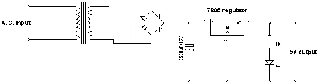
Voltage Regulation
The main function of a voltage regulator is to keep the output voltage of the DC supply constant even when there is a variation in the AC input voltage or if the load varies. The most
commonly used regulators are the three terminal integrated circuits. These linear regulators generate fixed voltages of 3V, 5V, 6V, 9V, 12V or 15V depending on the user’s choice.
The unregulated DC input voltage is applied to the input terminals and a regulated output voltage of 5v is gotten from the output terminals. The unregulated input voltage is filtered by the 1000µF.
The light emitting diode shown in the circuit diagram below serves as an indicator showing when the circuit is powered on. The 1KΩ resistor serves as a current limiter limiting the amount of current flowing into the LED and thus preventing it from damage. As a suitable current for the LED would be 0.005mA, the value of the resistor is calculated by dividing the regulator output voltage by the required current i.e.
5
0.005= 1000Ωor 1KΩ………6
The complete circuit diagram of the power supply is shown in figure 4 below.
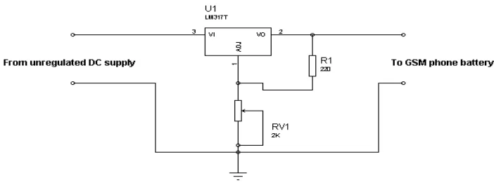
Battery Charging Unit In order to ensure that the GSM phone remains switched on, a means of charging its battery has Fig. 4: Circuit diagram of the power supply unit
to be incorporated. A simple battery charger circuit using the LM317 IC can be used to charge the battery. The LM317 IC is an adjustable voltage regulator and it has three terminals. Pin 1 of the IC is the control pin which is used to control the charging voltage. Pin 2 is the output pin from which the charging voltage is taken from. Pin 3 is the input pin to which the regulated DC supply is given. It is designed such that the charging voltage can easily be controlled with the aid of variable resistor.
It should be noted that the regulator drops a voltage of 3V across it hence the input voltage (VRinR) to it must be at least VRoutR plus 3V. The
maximum output current from the IC is 100mA. The ouput voltage (VRoutR) from the regulator is
given as
𝑉𝑜𝑢𝑡 = 1.25 �1 +𝑅𝑅21�+𝐼𝑎𝑑𝑗𝑅2…….7
Where IRadjR is small and is about 100µA
Making RR2Rthe subject formula gives:
𝑅2 =1𝑉.25𝑜−1.25
𝑅1+𝐼𝑎𝑑𝑗
………8
RR1R is fixed at 220Ω, while RR2R is a variable
resistor of 2kΩ.
The voltage produced by the GSM phone’s battery used is 3.7V and the rated battery capacity is 1000mAh, therefore a suitable charging voltage for it is 5V and a suitable charging current is 10% of 1000mAh i.e. 100mA which is the output current of the LM 317 IC. Putting these values into the equation above yields RR2R to be:
𝑅2 =1.255−1.25 240+0.0001
= 3.75
0.00578= 648.8Ω…..9
Hence the variable resistor RR2R is adjusted to be
648.8Ω. The battery charging circuit diagram is shown in figure 5 below.
Detection System
The detection system consists of a Light Dependent Resistor (LDR), resistors and a comparator. Resistors oppose the flow of current in a circuit. LDR is a sensor whose resistance decreases with increasing incident light intensity. The resistance of an LDR can range from 100Ω to 1MΩ. In accordance with Ohm’s law, a decrease in resistance is accompanied by a corresponding decrease in voltage and an
increase in resistance is accompanied by a corresponding increase in voltage.
A comparator compares two voltages connected to its inputs and produces a high or low at its output pin depending on which of the voltages is greater. The comparator used in this design is LM 358. The LM 358 is an 8-pin dual-in-line integrated circuit containing two independent, high gain operational amplifiers (OP-Amps) designed to operate from a single power supply Fig. 5: Battery charging circuit
over a wide range of voltages [4]. The internal circuit schematic of LM 358 is shown in figure 6.
RR1R and RR2R form a voltage divider network. The
voltage which is applied at the non-inverting input of the comparator is given as:
𝑉𝑟𝑒𝑓 =10 + 1010 ∗ 5 … … … .10
= 2.5V
This voltage is the reference voltage. The voltage across the LDR forms the input voltage. The variable resistor R3 is used to set the input voltage at a suitable level. In the absence of light, the resistance of the LDR is very high hence the voltage at the inverting input of the comparator is much, even greater than the voltage at the non-inverting input. This causes the output of the comparator to be low. On exposure to light, the resistance of the LDR decreases below 100KΩ. As a result ofthis, the voltage across the inverting terminal falls below half of the supply voltage and thus below the reference input voltage. This causes the output of the comparator to go high. This comparator output is connected to a transistor driver.
Transistor Driver
A transistor is a three terminal semiconductor device commonly used as amplifiers and switches. The most common type of transistor is
the bipolar junction transistor (BJT) and they are divided into NPN and PNP types.
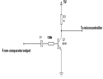
A transistor driver is used to switch the input to the microcontroller to either 5V or 0V in order to avoid the invalid voltage levels for TTL specifications which are from 0.8V to 2V [5].This is because the output of the comparator is not exactly 5V for a HIGH or 0V for a LOW. The voltage produced at the output of the comparator representing a HIGH is less than 5V and the voltage representing a LOW is more than 0V. As a result of this, the comparator output cannot be fed directly to the microcontroller. The transistor driver thus ensures that the voltage fed to the microcontroller is 5V for a HIGH and 0V for a LOW. The circuit diagram of the transistor driver is shown in figure 7.
From the datasheet of the BC547 transistor, the maximum collector current that the transistor can accommodate is 100mA above which the transistor gets damaged [6]. Also, the current gain hRfeR is 150. Since the transistor is being used
as a switch, it is operating either in the cut-off region or the saturated region with cut-off corresponding to the transistor being off, while saturated corresponds to the transistor being on. At saturation,
𝑉𝑐𝑐 = 𝐼𝑐 ∗ 𝑅𝐿… … … .11
Where IRcRis the collector current, RRLR is collector
resistance and VRccR is supply voltage. 𝑅𝐿=𝑉𝐼𝑐𝑐𝑐 … … … .12
Fig.7: Circuit diagram of the transistor driver Fig. 6: Circuit schematicLM 358
= 5𝑉
100𝑚𝐴… … … .13 = 50Ω
For clearer values representing 5V for a HIGH, a suitable value for RRL Ris 1kΩ since the collector
current can be less than the maximum specified value. Using 1kΩ as collector resistance yields collector current as:
𝐼𝑐 =𝑉𝑅𝑐𝑐𝐿=5𝑉1𝐾= 5mA……….14
This gives base current as:
𝐼𝐵 =ℎ𝑓𝑒𝐼𝑐 = 5𝑚𝐴150 = 0.033mA………….15
The base resistance is obtained from the equation:
𝑉𝑐𝑐=𝐼𝐵𝑅𝐵+ 𝑉𝐵𝐸… … … . … … . . .16
Where IRBR is the base current, RRBR is the base
resistance and VRBER is the base-emitter voltage
and it is 0.7V for silicon transistors. Hence RRB Ris 𝑅𝐵 = 𝑉𝑐𝑐−𝑉𝐵𝐸𝐼𝐵 = 5.0𝑉−0.7𝑉0.033𝑚𝐴 = 129kΩ……….17
The value of the resistor available in the market closest to 129kΩ is 130kΩ. So 130kΩ resistor was used instead.
Since the voltage from the comparator that corresponds to a LOW is greater than 0V, feeding it directly to the transistor may cause biasing even though that isnot the intended action. The 3V zener diode ensures that only voltages higher than 3V are allowed to pass and bias the transistor. RR2R is the base resistor while
RR1R is the collector resistor. RR1R also acts as a
pull-up resistor, pulling the collector to 5V when the transistor is unbiased. The transistor here acts as a switch. When sufficient voltage is applied at the base-emitter junction, the transistor is switched on and GROUND (i.e. 0V) which is at the emitter also appears at the collector. Since the input to the microcontroller is taken from the collector, it is thus seen that only 5V and 0V can be fed to the microcontroller for use in its operation.
Microcontroller
A microcontroller is a single integrated chip or circuit which has features like processor, memory, and input/output pins [7]. It is also known as a miniaturized computer in the sense that it has input and output, central processing unit, random access memory (RAM) and read only memory (ROM). It is a programmable
memory device which accepts hexadecimal code and produces an output according to the instruction written in either embedded C language or assembly language.
The microcontroller used for this paper is AT89C52. It has 8kB of on-chip ROM, 256 bytes of on-chip RAM, 4.0V-5.5V operating range, 32 programmable I/O lines, six interrupt sources. It contains the control program and its function is to co-ordinate all the activities of the entire system.
U
Serial Communication in Microcontroller
Serial communication is often used either to control or to receive data from an embedded microprocessor [8]. It is a form of input/output communication in which the bits of a byte are transferred one after the other in a timed sequence on a single wire. The rate of data transfer in serial data communication is stated in bits per second (bps). Another widely used terminology for bps is the baud rate. It is a modern terminology and is defined as the number of signal changes per second. Error-free serial communication requires that the baud rate, number of data bits, number of stop bits, and presence or absence of a parity bit be the same at the transmitter and at the receiver.
Serial communication in AT89C52 microcontroller is achieved via pins P3.0 (for receiving data) and P3.1 (for transmitting data). All modes in serial communication are controlled through Serial Control Register (SCON). SCON is an 8-bit register used to program the start bit, stop bit, and data bits of data framing among other things[9].
GSM Modem
Since the phone at the meter side will send message to a computer at the power distribution area, there is a need for a GSM modem. A GSM modem is a wireless device that works with a GSM wireless network.It operates over a subscription to a mobile operator. A wireless modem behaves like a dial-up modem. The main difference between them is that a dial-up modem sends and receives data through a fixed telephone line while a wireless modem sends
and receives data through radio waves. From the mobile operator perspective, a GSM modem looks just like a mobile phone. When a GSM modem is connected to a computer, this allows the computer to use the GSM modem to communicate over the mobile network. While these GSM modems are most frequently used to provide mobile internet connectivity, many of them can also be used for sending and receiving SMS and MMS messages.
Computers use AT commands to control modems (AT means attention). Both GSM modems and dial-up modems support a common set of standard AT commands. With these AT commands, you can do things likereading, writing and deleting SMS messages; sending SMS messages; monitoring the signal strength.
GSM USB Cable
The USB cable is used in connecting the GSM phone to a computer. It consists of two terminals; one is a USB connector which is
plugged into the USB port of a computer while the other terminal is connected to the GSM phone. However, since the GSM phone is to be connected to a microcontroller, the USB terminal of the cable is cut off. The USB cable consists of five wires within it, two of which are used for serial communication with the microcontroller. For this paper, only three out of these five wires are used. Two are for data transfer and the remaining wire is connected to ground. The other two wires are left unconnected.
The flowchart
2T
A flowchart is a software algorithm that represents the pattern of a system of operation and it gives the designer an appropriate picture of the system performance and pattern. The flowchart of the system is represented in figure 8 below:
Fig. 8: Flowchart showing the operation of the system
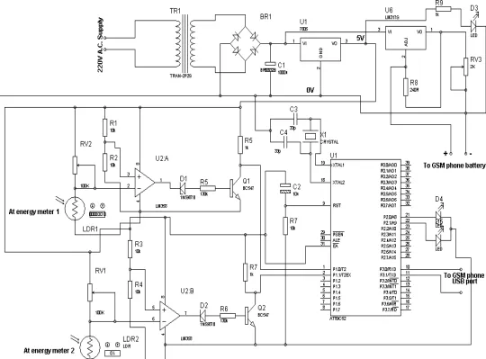
The Circuit diagram
The circuit diagram of the system is presented in figure 9 below.
Principle of Operation
The design of a microcontroller based power theft identifier is achieved using the AT89C52 microcontroller. The codes are used such that when a particular bit of the microcontroller is low, the microcontroller forwards a pre-programmed message into the GSM phone which then sends this message in form of text to
a particular phone number. The sensors (LDRs) are connected to port 1 of the microcontroller through an operational amplifier which is configured as a comparator. The sensors function as the eye of the microcontroller, which detect any attempt at energy theft. When the intensity of the light falling on the LDR increases, its resistance decreases. The sensors are connected to the inverting terminal of the Fig. 9: Circuit diagram of the Microcontroller Based Power Theft Identifier
comparators. The comparators are configured in such a way that their outputs remain low when the energy meter is not opened that is when the intensity of light falling on the sensor is low. The non-inverting terminals of the comparators are configured to have a certain fixed voltage across them. When the meter is opened, light falls on the sensor and its resistance decreases causing a subsequent decrease in the voltage across the inverting terminal of the comparator. The voltage across the inverting terminal now falls below the voltage across the non-inverting terminal. This causes the output of the comparator to go HIGH. This HIGH output activates the transistor driver which switches the input to the microcontroller to zero (LOW). Using the program written and embedded into the microcontroller, when a low is received as a bit, the microcontroller thus `notices’ that the meter has been opened and then sends the appropriate message to the GSM phone via its serial communication pins i.e. pins 10 and 11. The GSM phone on reception of this message then sends it out as SMS to the required destination computer in the energy distribution area. The light emitting diodes (LEDs) DR4R and
DR5R indicate when GSM phone is sending
messages as a result of opening meter 1 and meter 2 respectively. LED R3R indicates when the
system is powered on.
Conclusion
In this paper, the principle of detecting power theft is based on the concept of electro-optical
sensing. The system utilized AT89C52
microcontroller as well as a GSM phone for its operation. With such a system implemented in real time, the need for regular vigilance can be avoided and power can be supplied at the economical rate, thereby improving the economy of a country.
Recommendation
The quest for an energy theft detection system has led to many researches geared towards finding ways to prevent or reduce energy theft. The design of the microcontroller based power theft identifier system can still be improved in
some ways. The proposed improved measures are listed below and this could serve as a means of aiding researchers to carry out similar or related works.
(1) In addition to the power theft information, a means of transmitting data indicating the used energy(number of units) can be incorporated into the system. If this is done, then there will be no requirement for data collection (a lot of man power can be saved).
(2) A two-way communication can be designed in such a way that a signal from Power distribution areacan be transmitted which disconnects the main line from meter if a user is unable to pay his/her bill ontime or if the user is attempting power theft.
References
[1] Schuster A., “Microcontroller Principles and Applications”, Maxon Press Ltd, Rochester, 2008.
[2] “Power Supply Design”, Retrieved from36TUhttp://engknowledge.com/power_supply_de
sign.aspxU36T
[3] Theraja B. L and Theraja A.K., “A Textbook of Electrical Technology”, S. Chand & Company Ltd, New Delhi, 2008.
[4]Allurkar R.S.,”Logic Designs”, CBS publishers and Distributors, New Delhi, 2009. [5] Ezeh K.C., “Fundamentals of Electronics Designs”, 2P
nd
P
Edition, Madonna Printers and Publishers, Awka, 2013.
[6]“BC 547 General Purpose Transistor Datasheet”,Retrieved from
36TU
http://www.datasheetcatalog.comU36T
[7]Predko Myke, “Handbook of
Microcontrollers”, McGraw Hill, New York, USA, 2007.
[8] “Serial Communication”, Retrieved from
36TU
http://esd.cs.ucr.edu/labs/serial/serial.htmlU36T
[9] Douglas V.H., “Microcontrollers and Interfacing: “Programming Hardware” McGraw Hill Inc, New York, 2008.