Scholarship@Western
Scholarship@Western
Electronic Thesis and Dissertation Repository
7-11-2013 12:00 AM
Three-Phase Reduced Switch Topologies for AC-DC Front-End and
Three-Phase Reduced Switch Topologies for AC-DC Front-End and
Single-Stage Converters
Single-Stage Converters
Dunisha Wijeratne
The University of Western Ontario
Supervisor
Gerry Moschopoulos
The University of Western Ontario
Graduate Program in Electrical and Computer Engineering
A thesis submitted in partial fulfillment of the requirements for the degree in Doctor of Philosophy
© Dunisha Wijeratne 2013
Follow this and additional works at: https://ir.lib.uwo.ca/etd
Part of the Controls and Control Theory Commons, Electrical and Electronics Commons, and the
Power and Energy Commons
Recommended Citation Recommended Citation
Wijeratne, Dunisha, "Three-Phase Reduced Switch Topologies for AC-DC Front-End and Single-Stage Converters" (2013). Electronic Thesis and Dissertation Repository. 1361.
https://ir.lib.uwo.ca/etd/1361
This Dissertation/Thesis is brought to you for free and open access by Scholarship@Western. It has been accepted for inclusion in Electronic Thesis and Dissertation Repository by an authorized administrator of
FOR AC–DC FRONT–END
AND SINGLE–STAGE CONVERTERS
(THESIS FORMAT: Monograph)
by
Dunisha Wijeratne
Graduate Program in Engineering Science Department of Electrical and Computer Engineering
A Thesis Submitted in Partial Fulfillment
of the Requirements for the Degree of Doctor of Philosophy
The School of Graduate and Postdoctoral Studies The University of Western Ontario
London, Ontario, Canada
Abstract
Conventional three-phase AC-DC converters have two converter stages. They have a
front-end converter that converts the input AC voltage into an intermediate DC bus voltage
and a second, back-end converter that converts this DC bus voltage into the desired isolated
DC output voltage. The front-end converter also performs power factor correction (PFC) and
shapes the three-phase input currents so that they are nearly sinusoidal and in phase with the
three-phase input voltages. This allows the AC power source to be used in the most efficient
manner.
The front-end AC-DC converter is typically implemented with six switches while the
back-end DC-DC converter is typically implemented with a four switch DC-DC full-bridge
topology. Power electronic researchers have been motivated to try to reduce the number of
switches that are used in the conventional two-stage approach in order to reduce cost and
simplify the overall AC-DC converter. There are two general approaches to doing this: This
first approach is to reduce the number of switches in the front-end AC-DC converter. The
second approach is to combine the AC-DC converter and the DC-DC converter in a single
converter so that the overall AC-DC converter can be implemented in a single converter
stage that can simultaneously perform AC-DC power conversion with PFC and DC-DC
power conversion.
The main focus of this thesis is on new power converter topologies that convert a
three-phase AC input voltage into an isolated DC output voltage with a reduced number of
switches. In the thesis, a new family of reduced switch front-end converter topologies is
proposed, an example converter from this new family is selected for further study and a
two new three-phase AC-DC single-stage converters are proposed and their properties and
characteristics are compared. For each new converter that is investigated in detail, its modes
of operation are explained, its steady-state characteristics are determined by mathematical
analysis, and the results of the analysis are used to develop a design procedure that can be
used to select key components. The design procedure of each new converter is demonstrated
with an example that was used in the implementation of an experimental prototype that
confirmed the feasibility of the converter.
The thesis concludes by presenting that have been reached as a result of the work that was
performed, stating its main contributions to the power electronics literature and suggesting
future research that can be done based on the thesis work.
KEYWORDS: Three-phase rectification, AC-DC conversion, power factor correction,
reduced-switch converters, multilevel converters, soft-switching, three-phase power
Acknowledgments
I would like to acknowledge and thank my supervisor Dr. Gerry Moschopoulos for his
encouragement, very valuable analytical, practical and academic guidance and advice
throughout in all aspect of my research and in writing and publishing of thesis. I am also
thankful to the members of my examination committee.
I also appreciate the support given by Dr. S. Kumarawadu and Dr. J. Samarabandu from
the very initial stage of my academic life.
Further I wish to recognize and admire the guidance and support given by especially,
Eugen Porter in the Machines Shop and many others, including the administrative staff of the
ECE department of UWO.
Finally I would like to record my deepest gratitude to my late-father Indra for his
unrelenting encouragement and help for me to continue my higher education, sincere thanks
to my fiancé Niroshan, to my uncles Chandra and Sam for motivating and encouraging me
throughout my studies.
And last but not least, I am thankful to my loving mother Indira and to my Aunt Sandhya
for the endless love that they have given me.
Dunisha Wijeratne
Dedication
This Thesis is dedicated to my loving late-father Indra and mother Indira.
Without their love, wisdom, and guidance, I would not have the realized my goals to
Table of Contents
Abstract ... ii
Acknowledgments ... iv
Dedication ... v
Table of Contents ... vi
List of Tables ... x
List of Figures ... xi
List of Nomenclature ... xvi
List of Abbreviation ... xviii
Chapter 1 ... 1
1 Introduction to Thesis ... 1
1.1 Introduction ... 1
1.2 Three-Phase Two-Stage Power Factor Correction ... 2
1.2.1 DC-DC Full-Bridge Converter ... 3
1.2.2 Three-Phase AC-DC Front-End Converters ... 5
1.3 Three-Phase Single-Stage PFC ... 8
1.4 Thesis Objectives ... 11
1.5 Thesis Outline ... 11
Chapter 2 ... 14
2 Three-Phase Multilevel Front-End Converters ... 14
2.1 Introduction ... 14
2.2 Review of Operation of Basic Three-Phase Single-Switch Converters (TPSSCs)14 2.2.1 Converters with an Inductive Input Filter ... 15
2.2.2 Converters with a Capacitive Input Filter ... 17
2.4 Multilevel Converters with Flying Capacitor ... 19
2.5 Converters with Neutral Point Connection ... 21
2.6 Conclusion ... 25
Chapter 3 ... 27
3 A Novel Three-Phase Neutral Point Connected Buck-Boost AC-DC Converter ... 27
3.1 Introduction ... 27
3.2 Operation of the Proposed Converter ... 27
3.2.1 D < 0.5 [Buck mode of operation] ... 29
3.2.2 D > 0.5 [Boost mode of operation] ... 32
3.3 Steady-State Analysis ... 39
3.3.1 Analysis for Buck mode of operation (D < 0.5) ... 39
3.3.2 Analysis for Boost mode of operation (D > 0.5) ... 49
3.4 Design and Example ... 52
3.5 Experimental Results ... 58
3.6 Conclusion ... 63
Chapter 4 ... 65
4 A Three-Phase Neutral Point Connected Buck-Boost Quasi-Resonant Ac-Dc Converter ... 65
4.1 Introduction ... 65
4.2 Soft-Switching ... 65
4.3 Operation of the Proposed Converter ... 67
4.3.1 D < 0.5 [Buck mode of operation] ... 68
4.3.2 D > 0.5 [Boost mode of operation] ... 73
4.4 Mathematical Analysis ... 77
4.4.1 Quasi-Resonant Criterion ... 79
4.4.3 Input Power Factor Correction (PFC) Criterion ... 80
4.5 Design and Example ... 84
4.6 Experimental Results ... 90
4.7 Conclusion ... 95
Chapter 5 ... 97
5 A Three-Phase Single-Stage AC-DC PWM Buck-Type Full-Bridge Converter ... 97
5.1 Introduction ... 97
5.2 A Three-Phase Single-Stage AC-DC PWM Buck-Type Full-Bridge Converter .. 98
5.3 Operation of the Proposed Converter ... 101
5.4 Converter Analysis ... 109
5.5 Design and Example ... 115
5.5.1 Selection of Turns Ratio n ... 116
5.5.2 Determination of Duty Ratio D and Input Capacitors Ca, Cb, Cc ... 117
5.5.3 Design of the ZVZCS Passive Auxiliary Circuit ... 120
5.5.4 Design Determination of Input Inductors La, Lb, Lc ... 120
5.6 Experimental Results ... 122
5.7 Conclusion ... 126
Chapter 6 ... 128
6 Comparison of Two Buck–Type Three–Phase Single–Stage AC–DC Full Bridge Converters ... 128
6.1 Introduction ... 128
6.2 Steady-State Operation of Converter #2 ... 128
6.3 Analysis of Converter #2 ... 135
6.4 Design Procedure of Converter #2 ... 137
6.4.1 Selection of Turns Ratio n ... 137
6.4.3 Determination of Leakage Inductance Llk and Auxiliary Capacitor Cx .. 143
6.4.4 Determination of Input Inductors La = Lb = Lc ... 144
6.5 Experimental Results of Converter #2 ... 145
6.6 Features of Single-Stage Full-Bridge Type Converters ... 148
6.6.1 Converter # 1 ... 148
6.6.2 Converter # 2 ... 149
6.7 Conclusion ... 151
Chapter 7 ... 152
7 Conclusion ... 152
7.1 Introduction ... 152
7.2 Summary ... 152
7.3 Conclusions ... 155
7.4 Contributions ... 157
7.5 Future Work ... 157
References ... 159
List of Tables
Table 2.1: Peak switch voltage stress equations for TPSSCs. ... 18
Table 2.2: Peak switch voltage stress equations for FCMCs. ... 21
Table 3.1 IEC 61000–3–2 Class A standard limits, harmonics of phase current for loads 2 kW–500W and PF when V2 = 150V. ... 61
Table 3.2: IEC 61000–3–2 Class A standard limits, harmonics of phase current for loads 2 kW–500W and PF when V2=500 V ... 62
Table 4.1 IEC 61000–3–2 Class A standard limits, harmonics of phase current efficiency values Vo/Po combinations. ... 94
Table 5.1: IEC61000-3-2CLASS A,INPUT CURRENT HARMONICS,POWER FACTOR AND
EFFICIENCIES ... 125
List of Figures
Fig 1.1: Three–phase AC–DC six switch two–stage full–bridge converter [1]. ... 3
Fig 1.2 Three–phase AC–DC six switch two–stage full–bridge converter. ... 3
Fig 1.3(a): Three-phase AC-DC six switch two-stage full-bridge converter. ... 3
Fig 1.4(b): Phase-shift PWM switching scheme and full-bridge converter waveforms. ... 4
Fig 1.5: Three-phase AC-DC converter using three single-phase modules. ... 6
Fig 1.6: Reduced switch three-phase AC-DC converters. ... 7
Fig 1.7: Three–phase AC–DC single–switch boost front-end converter. ... 8
Fig 1.8: Three–phase AC–DC single–switch boost rectifier and DC–DC full–bridge converter... 9
Fig 1.9: Examples of previous three-phase AC-DC single-stage converters. ... 10
Fig 2.1: Three-phase single-switch PFC converters. ... 16
Fig 2.2: (a) Discontinuous input inductor current (b) Discontinuous input capacitor voltage. ... 17
Fig 2.3: One leg of two-level multilevel converters. ... 19
Fig 2.4: Multi-level reduced switch converters with a flying capacitor. ... 20
Fig 2.5: Synthesis of an example flying capacitor multilevel converter – Buck-boost FCMC. ... 22
Fig 2.6: Synthesis of an example flying capacitor multilevel converter - Ćuk FCMC. ... 22
Fig 2.7: Multi-level reduced switch converters with neutral point connection. ... 24
Fig 2.9: Synthesis of an example flying capacitor multilevel converter - Buck-boost NPCMC.
... 26
Fig 3.1: Proposed three-phase AC-DC two-switch NPCMC. ... 28
Fig 3.2: Modes of the converter when D < 0.5. ... 31
Fig 3.3: Typical waveforms when D < 0.5. ... 33
Fig 3.4: Modes of the converter when D > 0.5. ... 36
Fig 3.5: Typical waveforms when D > 0.5. ... 38
Fig 3.6: Dc-DC single-switch LC filter buck-boost converter. ... 41
Fig 3.7: Modes of operation of converter in Fig. 3.6 when D < 0.5. ... 42
Fig 3.8: Typical waveforms for DC-DC buck-boost converter when D < 0.5. ... 45
Fig 3.9: Three-phase AC-DC single-switch buck-boost converter. ... 46
Fig 3.10: Typical input capacitor voltages for a switching cycle when D < 0.5. ... 49
Fig 3.11: Flowchart of mathematical analysis. ... 53
Fig 3.12: Voltage conversion ratio (M) vs. duty ratio (D) for the proposed converter when D < 0.5. ... 55
Fig 3.13: Single-phase equivalent L-C filter circuit. ... 56
Fig 3.14: Phase voltage and line current Po,max = 2 kW [V: 100 V/div, I: 10 A/div, t: 10 ms/div]. ... 58
Fig 3.15: Input capacitor phase voltage for line cycles Po,max = 2 kW[V: 1200 V/div, t: 4 ms/div]. ... 59
Fig 3.17: Input current and voltage when V2 = 150 V [V: 100 V/div, I: 10 A/div, t: 10 ms/div].
... 61
Fig 3.18: Phase current and voltage when V2 = 500 V for loads [V: 100 V/div, I: 10 A/div, t: 10 ms/div]. ... 62
Fig 3.19: Switch voltage and current for V2: (a) 150 V, (b) 500 V when Po,max = 2 kW. ... 63
Fig 3.20: Efficiency curves buck mode boost mode at load conditions. ... 64
Fig 4.1: Non-ideal (hard) switching characteristics [1]. ... 66
Fig 4.2: The proposed three-phase, multilevel, quasi-resonant buck-boost converter. ... 67
Fig 4.3: Modes of the converter when D < 0.5. ... 71
Fig 4.4: Typical waveforms when D < 0.5. ... 73
Fig 4.5: Modes of the converter when D > 0.5. ... 77
Fig 4.6: Typical waveforms when D > 0.5. ... 78
Fig 4.7: Flowchart to select operating points. ... 83
Fig 4.8: Input PFC and voltage gain - Design curves. ... 88
Fig 4.9: ZCS operation – Design curves. ... 90
Fig 4.10: Phase voltage and line current Po = 2 kW, V2 = (a) 150 V and (b) 500 V [V: 100 V/div, I: 10 A/div, t: 10 ms/div]. ... 91
Fig 4.11: Input capacitor phase voltage for line cycles Po = 2 kW, V2 = (a) 150 V and (b) 500 V [V: 1000 V/div, t: 4 ms/div]. ... 92
Fig 4.12: Input capacitor phase voltage for line cycles Po = 2 kW and V2 = (a) 150 V, (b) 500 V [V: 750 V/div, t: 10 µs/div]. ... 92
Fig 4.14: Input current and voltage when Vo = 500 V and Po = (a) 2 kW and (b) 500 W [V:
100 V/div, I: 10 A/div, t: 10 ms/div]. ... 94
Fig 4.15: Switch voltage (VS) and Current (IS) for Po = 2 kW (a) V2 = 150 V and (b) Vo = 500 V [V: 100 V/div]. ... 95
Fig 5.1: Three-phase single-stage buck-type full-bridge converter. ... 99
Fig 5.2: AC-DC single-switch buck rectifier and DC-DC full-bridge converter ... 100
Fig 5.3: Modes of steady-state operation. ... 107
Fig 5.4: Typical waveforms of the converter under study. ... 108
Fig 5.5: Characteristic curves. ... 118
Fig 5.6: Single-phase equivalent L-C filter circuit. ... 121
Fig 5.7: Experimental Input voltage and current. ... 122
Fig 5.8: Input capacitor phase voltage Po = (a) 1.92 kW and (b) 0.4 kW (vCa = 500 V/div, t = 4 ms/div). ... 123
Fig 5.9: Input capacitor phase voltage Po= (a) 1.92 kW and (b) 0.4 kW (vCa = 250 V/div, t = 10 µs/div). ... 123
Fig 5.10: Experimental waveforms. ... 124
Fig 5.11: Three-phase AC-DC single-stage isolated boost converter. ... 126
Fig 6.1: Three–phase AC–DC, single–stage buck–type full–bridge converter. ... 129
Fig 6.2: Three–phase AC–DC, single–stage modified buck–type full–bridge converter [55]. ... 129
Fig 6.3: Modes of operation of Converter #2 at steady–state. ... 134
Fig 6.5: Design curves. ... 142
Fig 6.6: Phase voltage and phase current (Va = 100 V/div, Ia= 7.5 A/div, t = 10 ms/div). ... 146
Fig 6.7: Input capacitor phase voltage for Po= (a) 1.92 kW, (b) 400 W ... 147
Fig 6.8: Input capacitor phase voltage when Po= 1.92 kW ... 147
Fig 6.9: Voltage and current of the leading leg switch when, Po = (a) 1.92 kW and (b) 400 W
(Vs= 300 V/div, Is = 20 A/div, t = 10 µs/div). ... 148
Fig 6.10: Voltage and current of the lagging leg switch when, Po = (a) 1.92 kW, (b) 400 W
(Vs = 300 V/div, Is = 20 A/div, t = 10 µs/div). ... 148
List of Nomenclature
Ca, Cb, Cc Input Capacitors Cbus Dc bus capacitor
Cfly Flying capacitor
Co Output capacitor
Cx Auxiliary capacitor on transformer secondary side
D Switch duty cycle
Do1, Do2 Output diode
Dx Diode
fl Line frequency
fr Dominant harmonic frequency (sidebands) related to the switching frequency
fs Switching frequency
Ia Line current
ibus Bus current
iCa,k Instantaneous input capacitor current
ifb Full-bridge current
Ilfr High frequency input ripple current in to the utility side
iLlk Instantaneous current through leakage inductor
ILo Output inductor current
Io Dc output current
Irms Input rms line current
La, Lb, Lc Input inductors
Llk Leakage inductance
Lo Output inductor
Lx Inductor
M Output-to-input voltage conversion ratio
n Transformer turns ratio
npri No. of turns in the primary winding
nsec No. of turns in the secondary winding
S Switch
T Transformer
Tl Line period
ton Switch On time
Ts Switching Period
vCa,k Instantaneous input capacitor voltage in kth switching cycle VCa,ave Average voltage of capacitor Ca
VCa,pk Peak voltage of capacitor Ca
vCa,k Instantaneous voltage of Ca in kth switching cycle VCM Peak capacitor voltage
VCfly Voltage across flying capacitor
vCx,k Instantaneous voltage of Cx in kth switching cycle
Vdc DC voltage (source)
vD Voltage across diode D
Vg1, Vg2 Gate pulse of switch S1, S2 vLa,k Voltage across input inductor Lbus Dc bus inductor
vCx,k Instantaneous voltage across auxiliary capacitor Cx Vll,rms Three-phase line-line rms voltage
vLbus Instantaneous voltage across bus inductor
Vo Output voltage
vrec,k Instantaneous output voltage of three-phase diode rectifier in kth switching cycle
VS,pk Peak switch voltage
Wi Total input energy
Wa Input energy of phase A
Wo Output energy
List of Abbreviation
AC Alternating current
CVM Continuous voltage mode
DC Direct current
DVM Discontinuous voltage mode
FCMC Flying capacitor multilevel converter
FFT Fast Fourier transform
IGBT Insulated gate bi-polar transistor
MOSFET Metal oxide field effect transistor
NPCMC Neutral-point connected converters
PF Power factor
PFC Power factor correction
PWM Pulse width modulation
QR Quasi-resonant
TPSSC Three-phase single switch converter
ZCS Zero-current switching
ZVS Zero-voltage switching
Chapter 1
1
Introduction to Thesis
1.1 Introduction
Power electronic converters use active semiconductors (e.g. IGBTs) and passive power semiconductors (e.g. diodes) and passive elements (e.g. inductors and capacitors) arranged in circuit structures to convert power from the form available from a source to that required by a load. The power source may be a DC source, a single–phase AC source, or a three-phase AC source with line frequency of 50, 60 or 400 Hz. It may also be an electric battery, a solar panel, an electric generator or a commercial power supply. The source feeds the input of the power converter, which converts the input power to the required form for a load. The load may be DC or AC, single–phase or three–phase, and may or may not need transformer isolation from the power source. The power converter, therefore, can be an AC/DC converter, a DC/DC converter, a DC/AC inverter or an AC/AC converter depending on the application.
The main focus of the research in this thesis has been on three-phase AC-DC power converters. These are converters that convert a three-phase input voltage into an isolated DC output voltage. The three-phase AC voltage is typically obtained from the utility mains. Ac-DC power converters connected to the mains voltage can generate and inject current harmonics into the utility mains. Injecting current harmonics into the AC mains results in two significant consequences:
First, because of the finite impedances of the power lines, harmonic currents
generate voltage variations at the point of common coupling that other equipment on the line must tolerate.
Second, although current harmonics do not generate real power, they must be
As a result, regulatory bodies have imposed strict limits on the harmonics that power converter can inject into the utility mains.
To minimize the harmonics generated by power converters, power factor correction (PFC) techniques have been developed so that the generated harmonics comply with regulatory agency standards such as IEC 61000-3-2 Class A. Power factor (PF), which is a measure of how effectively the input AC source is used can be defined as
rms ) rms (
ll I
V 3
P
PF (1.1)
where P is the output real power, Vll,rms is the three-phase line-line rms voltage and Irms is
the input rms line. A power factor of 1 is the maximum power factor that can be achieved and represents the most efficient use of the input AC source.
AC-DC power converters implemented with PFC techniques are made to operate in such a way that their input currents are shaped so that they are sinusoidal and in phase with their respective phase voltages. Most AC-DC power converters today that are supplied by the AC mains are implemented with some sort of PFC technique and the implementation of PFC in power electronic converters is a very relevant research topic in the power electronics field.
1.2
Three-Phase Two-Stage Power Factor Correction
1.2.1
DC-DC Full-Bridge Converter
The DC-DC full-bridge converter topology shown in Fig. 1.3(a) is the standard topology that is used for higher power DC-DC power conversion (> 500 W). The
converter consists of four switches (S1 - S4), a transformer (T), two output diodes (D1,
D2), an inductor (Lo) and a capacitor (Co); the load is represented as a resistor. The
converter works as follows: voltage is impressed across the primary of the transformer
Ac-dc Rectification 1Φ or 3Φ ac
power input
Dc-dc Conversion Intermediary
dc voltage
Dc power Output
Stage 1 Stage 2
Fig 1.1: Three–phase AC–DC six switch two–stage full–bridge converter [1].
.
.
R
Six-Switch AC-DC PFC Rectifier
DC-DC Converter
C o S 7
.
L o
Stage 1 Stage 2
C bus
S 10
S 9
S 8 S 1 S 3 S 5
S 4 S 6 S 2
Fig 1.2 Three–phase AC–DC six switch two–stage full–bridge converter.
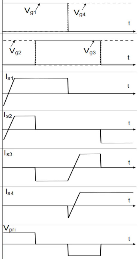
winding whenever a diagonally opposite pair of switches are on (S1 and S2 or S3 and S4); the polarity of the voltage depends on the pair of switches that is on. No voltage is impressed across the transformer primary whenever current flows through two top switches (or their body-diodes) or two bottom switches (or their body diodes). Typical switch gating signals and a typical primary voltage waveform are shown in Fig. 1.3(b).
Each converter switch is on for 50% of the switching period and there is no overlap
between the gating signals of the two switches in each leg, to avoid short-circuiting. The output voltage is controlled by shifting the gating signals of the switches in one leg with respect to those of the switching in the other leg, which controls the length of time voltage is impressed across the transformer. The converter can be said to be in a power transfer mode whenever a voltage is impressed across the transformer primary and appears at the secondary, and to be in a freewheeling mode when there is no voltage across either transformer winding and current just flows (“freewheels”) throughout the converter. The primary voltage waveform is an AC waveform that is stepped down or up (typically down), rectified by the two secondary output diodes, then filtered by a
low-pass filter formed by Lo and Co to produce the required output DC voltage.
1.2.2
Three-Phase AC-DC Front-End Converters
The front-end converter converts the three-phase input voltage into an intermediate DC bus voltage while simultaneously performing some sort of PFC technique to ensure an input power factor as close to unity as possible. The use of six-switch front-end rectifiers such as the one shown in Fig. 1.2 is the standard when implementing PFC in three-phase AC-DC PFC. For the front-end converter shown in Fig. 1.2, PFC is performed by sensing the three-phase input voltages and currents and then turning the converter switches on and off in an appropriate manner so that the current in each phase is nearly sinusoidal and in phase with the corresponding phase voltage. Numerous PFC schemes for three-phase front-end converters have been proposed [2]-[4], but they will not be reviewed here as they are outside the scope of this thesis.
1.2.2.1
Modular PFC Method
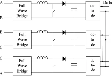
One alternative to the standard six-switch three-phase AC-DC rectifier is to use three separate single-phase boost PFC converter modules as shown in Fig. 1.4 [5]-[8]. Each module in Fig 1.4 is a two-stage converter consisting of PFC boost front-end converter followed by a DC-DC back-end converter to get the desired bus voltage. The main advantage is that existing single-phase modules can be used, which are popular and widely available and do not require knowledge of sophisticated three-phase control. The main disadvantages are the need to synchronize the operation of each individual module to the others, the presence of triplen harmonics due to parametric variations in the modules, and the high number of components.
1.2.2.2
Reduced Switch Front-End Converters
Several researchers have proposed front-end AC-DC converters with a reduced number of switches, less than six switches typically found in conventional front-end converters [9]-[10]. Two of the more popular converters of this type are briefly explained below.
Four-Switch Converter - The converter shown in Fig. 1.5(a) [9] is a four switch
converter that has two legs with two switches in each leg and a third leg that is
made with two capacitors (C1, C2). The midpoint of each leg is connected to a
phase of the three–phase source. The general principle behind this converter is that if the phase currents that are associated with the converter legs that have switches
A Dc bus
B
Full Wave Bridge
dc-to- dc
Full Wave Bridge
dc-to- dc B
C
Full Wave Bridge
dc-to- dc C
A
are controlled, then the third phase current will be constrained by the other two phase currents so that it too will be sinusoidal and in phase with the phase voltage.
Vienna Rectifier - The converter shown in Fig. 1.5(b) [10] has three main power
switches that are implemented with four diodes to each switch to make them bidirectional and allow current to flow through each direction. The converter can be operated like a conventional six-switch converter but with one bidirectional switch in each converter leg instead of two unidirectional switches.
Although reduced switch converters may be less expensive than six-switch converters, they require the use of control methods that are much more sophisticated than those used in conventional six-switch converters. These methods are not easy to implement and their performance merits are not clear when compared to conventional six-switch converters so that reduced switch converters are not widely used in the power electronic field.
1.2.2.3
Single-Switch Front-End Converters
For lower three-phase power applications, it is possible to perform PFC by using only a single switch [11]-[16] as the stress that is placed on the switch device is not excessive. The first such converter to be proposed was the three-phase single-switch AC-DC boost converter shown in Fig. 1.6 [11] as the front-end AC-DC converter of a two-stage
converter. The converter consists of three boost inductors (La, Lb, Lc), three-phase
diode-V dc/2
dc/2
V Vo S 1
S 3 S 4
S 2 +
-
+ -
C 1
C 2
(a). Four-switch front-end converter
S +
S - D F+
D F- D N+
D N-
S a C +
C -
(b). Vienna rectifier
bridge, switch (S), diode (D) and a filter capacitor (C); an input filter is used to filter out higher frequency harmonics that are created by the converter’s switching operation. The converter is simple as it only requires one switch operating with high switching frequency (> 5 kHz) and does not require any sensors to sense the input currents or any controller that is dedicated to ensure that the input voltages and currents are in phase. The converter needs just a single controller to regulate its output voltage. Although several switch front-end AC-DC converters have been proposed [15]-[16], the single-switch converter shown in Fig. 1.6 is by far the most popular single-single-switch front-end converter that is used for general applications and most other single-switch front-end converters are either variations of the converter shown in Fig. 1.6. or are limited to certain niche applications.
1.3
Three-Phase Single-Stage PFC
Although reduced switch front-end AC-DC converters can reduce the size and cost of conventional two-stage converters, two separate and independently controlled converters are still needed (Fig. 1.7). In order to reduce the cost and complexity associated with implementing two switch-mode converters, power electronics researchers have tried to combine the PFC function of the AC-DC front-end converter with the DC-DC conversion function of the full-bridge converter in a single converter [17]-[27]. Some frequently cited examples for three-phase single-stage converters (TPSSCs) are shown in Fig. 1.8. Each subfigure shows a different TPSSC topology. These converters are typically implemented with just a single controller to regulate the output voltage so that there is no controller to regulate the intermediate DC bus voltage and no controller to perform input
PFC; input PFC is done naturally as a function of the converter’s operation.
The design of a three-phase single-stage converter is challenging because the converter must simultaneously performing both PFC and DC-DC conversion over the entire load and input range with only a single controller and without additional input current sensing and DC bus voltage control. As a result, relatively little research has been successfully done in this area and a trade-off must be made between the simplicity of single-stage converters and the better performance of more expensive two-stage converters. TPSSC that have been previously proposed have at least one of the following drawbacks:
The converter uses a three single-phase full-bridge modular approach [6] (i.e. Fig.
1.8(a)). This is expensive and it is not easy to synchronize the operation of all three converters to produce sinusoidal input currents.
The input currents must be discontinuous in order for input power factor
correction to be achieved (i.e. Fig. 1.8 (b)-(d)). Converters such those proposed in [17]-[23] incorporate the principles of the three-phase single-switch boost converter proposed in [11] into their topologies. Although an excellent input power factor may be achieved, the peak current stress of the semiconductor devices is very high.
The input currents are distorted and contain a significant amount of low frequency
harmonics [21] (i.e. Fig. 1.8(c)) as the converter has difficulty performing PFC S 1
. . .
S 4
S 3
S 2
L o
C o
Single-Switch Ac-Dc PFC Rectifier Dc-Dc Full-Bridge Converter
C bus
S
D
L a
L b
L c
R
(a) [6]
(b) [18]
. . R
R1
R3 R2
R4 L5
C5
C6 La
Lb
Lc
(c) [21]
. R
S2
S3 S1
S4 Cin1
Cin2 La
Lb
Lc
Lm1
Llk1
D7 D6 D5
D8
Llk2
Lm2
and DC-DC conversion simultaneously, thus compromising the quality of the input waveforms and PF.
The converter must be controlled using very sophisticated techniques. This is
especially true of multilevel converters [24] - [27] (i.e. Fig. 1.8(c)) where the need to balance the voltages on the split capacitors at the DC bus is critical.
1.4 Thesis
Objectives
The main objectives of this thesis are as follows:
To propose new reduced switch stress three-phase AC-DC front-end PFC
converters.
To propose new three-phase AC-DC single-stage PFC converters.
To determine the properties and steady-state characteristics of these new
converters by mathematical analysis and by using software such as MATLAB.
To develop a design procedure for each new converter that can be used in the
selection of critical converter components.
To confirm the feasibility of each new converter with experimental results
obtained from proof-of-concept prototype converters.
1.5 Thesis
Outline
In addition to this chapter, this thesis comprised of six chapters. The outline of the thesis is as follows:
Chapter 3: An example converter from the new Neutral point connected multilevel converter family is considered for further examination. In this chapter, the operation of the example converter is explained in detail, its steady-state properties and characteristics are determined by mathematical analysis, and the results of the analysis are used to establish a design procedure for the selection of key component values. The design procedure is demonstrated with an example and the feasibility of the new converter is shown with experimental results that were obtained from a prototype converter that was designed according to the design example.
Chapter 4: A technique to decrease the power losses that are created by the turn on and off of the converter in Chapter 3 is proposed in this chapter. In this chapter, it is explained how so-called soft-switching techniques can reduce these power losses and one such technique is chosen for further study, as implemented in the converter of Chapter 3. this paper. Similar to Chapter 3, the operation of this new converter is explained and analyzed and a design procedure is developed and demonstrated with an example. Experimental results that confirm the feasibility of the converter are also presented.
Chapter 5: The main objective of this chapter is to examine the operation of a buck-based, three-phase, single-stage AC-DC full-bridge converter. In the chapter, the operation of this fundamental converter is explained and analyzed, and a procedure for the design of its key components is derived and demonstrated with an example. The performance and characteristics of the converter are shown with experimental results that have been obtained from a prototype and general concluding remarks comparing buck-based and boost-buck-based, three-phase, single-stage AC-DC full-bridge converters are made.
Chapter 2
2
Three-Phase Multilevel Front-End Converters
2.1 Introduction
Three-phase, single-switch AC-DC converters such as the ones discussed in Section 1.6 of the previous chapter are a simple and inexpensive solution for lower power applications that require three-phase input power as they require only a single power switch and can be implemented without using sophisticated control methods or input current sensing. The main drawback that has limited the widespread use of these converters is the peak voltage stress that must be placed on the main switching device. This peak voltage stress can be reduced if the single converter switch is replaced by two switches in a multilevel structure that exposes these devices to less peak voltage stress.
In this chapter, two types of multilevel converters are discussed – flying capacitor multilevel converters and neutral point connected multilevel converters. Most of the converters examined in this chapter have never been presented elsewhere. Flying capacitor multilevel converters (FCMCs) are usually used for DC-DC or DC-AC inverter applications whereas in the thesis they were synthesized for three-phase AC-DC applications. Furthermore, except for the boost neutral point connected multilevel converter (NPCMC), the other NPCMCs have not been introduced to the best of the author’s knowledge.
Topologies for both types of converters are presented, the conversion from a single-switch structure to a multilevel structure is shown, and the peak single-switch stresses of the converter switches in each type of multilevel converter structure is examined.
2.2
Review of Operation of Basic Three-Phase
Single-Switch Converters (TPSSCs)
the power electronics literature: buck, boost, buck-boost, Ćuk, Zeta and Sepic. When the DC source is replaced by a three-phase AC source and diode bridge as shown in Fig. 2.1, six fundamental TPSSCs can be formed. The power factor correction (PFC) of any of these TPSSCs can be done without sensing any input parameter and an additional controller, as it can occur automatically as a function of the converter’s natural switching operation. The converter can operate like a DC-DC single-switch converter with a switch
duty cycle (D) that can be considered to be fixed throughout the input line cycle.
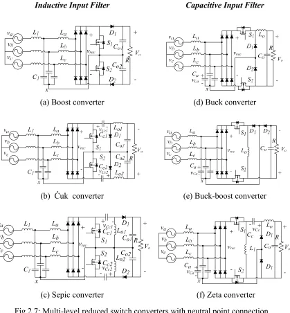
The six fundamental converters can be divided into two main groups:
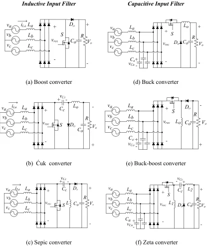
Converters with an inductive input filter (Boost, Ćuk and Sepic)
Converters with a capacitive input filter (Buck, Buck-boost and Zeta)
The converters with an inductive input filter ensure the input inductor currents (e.g. iLa)
rise and fall in every switching cycle whereas the converters with a input capacitive filter
ensure the capacitor voltages (e.g. vCa) rise and fall. The fundamental operation of an
example converter of each group is reviewed below.
2.2.1
Converters with an Inductive Input Filter
The single-switch boost converter shown in Fig. 2.1(a) is an example of a TPSSC with an inductive input filter. The converter operates as follows: The currents in all three input
inductors rise whenever the switch (S) is on and fall to zero whenever the switch is off.
This is shown in Fig. 2.2(a), where iLa is the current of input inductor La that rises from
zero to a peak value determined by the instantaneous phase A voltage when S is on (ton =
DTs). After S is turned off (toff = Ts[1-D)], iLa decreases from its peak value to zero and
remains at zero until S is turned on again. The input currents are discontinuous and are a
train of triangular pulses whose peaks are bounded by a sinusoidal envelope. This allows a nearly sinusoidal average current (current without high frequency ripple) to be achieved
in all three phases. The Ćuk (Fig. 2.1(b)) and Sepic (Fig. 2.1(c)) converters are the other
At the DC side of the boost converter, after the input diode bridge, the converter behaves as a typical DC-DC boost converter - the input inductors charge using the line
currents when S is on and feed the load when S is off [1]. When S is off, output diode Do
in Fig. 2.1(a) is forward biased, and as a result the output voltage (Vo) is placed across S;
Inductive Input Filter Capacitive Input Filter
(a) Boost converter
o o
a
b
c
a
b
c
a
o
Ca
o rec
(d) Buck converter
(b) Ćuk converter (e) Buck-boost converter
(c) Sepic converter
o o
a
b
c
a
b
c
a
1
c 2
Ca
Cc
o rec
(f) Zeta converter
thus the peak boost converter switch voltage is stress VS,pk= Vo. The peak switch voltages of the other TPSSCs with input inductive filter are given in Table 2.1.
2.2.2
Converters with a Capacitive Input Filter
The single-switch buck converter shown in Fig. 2.1(d) is an example of a fundamental TPSSC with a capacitive input filter. The converter operates as follows: When the switch
(S) is off, each of the three input capacitors (Ca, Cb, Cc) are charged to a level that is
proportional to the input line-to-line voltage that is placed across it. When S is turned on,
each input capacitor is completely discharged and remains at zero until S is turned off
again. The rise and fall of an input capacitor voltage is shown in Fig. 2.2(b), where vCa is
the instantaneous voltage of Ca – the input capacitor for phase A - and VCa,ave is the
average value (voltage without the high frequency ripple) of the discontinuous voltage
vCa. An excellent input power factor (PF) can be achieved if the converter is made to
operate with discontinuous input capacitor voltages.
Doing so ideally causes these voltages to be sinusoidal with high frequency components that are blocked by the input inductors so that the input phase currents are also sinusoidal with few if any high frequency components. This is because the voltage is a train of triangular pulses whose peaks are bounded by a sinusoidal envelope. The buck-boost [Fig. 2.1(e)) and Zeta [Fig. 2.1(f)] converters are the other two fundamental
(a)
(b)
TPSSCs with a capacitive input filter. The input capacitor voltages of both these converters can be shaped so that they are discontinuous and bounded by a sinusoidal envelope just like the buck converter.
While the input capacitors are being charged and discharged, the output section of the converter operates in the exact same manner as a standard DC-DC buck converter [1].
The peak voltage stress of S in the buck converter equals the line-line voltage of input
capacitors. VS,pk = √3vCa,pk, where VCa,pk is the peak phase voltage of Ca. The peak switch
voltages of the other TPSSCs with input capacitive filter are given in Table 2.1.
2.3 Multilevel Three-Phase Reduced-Switch Converters
The main power switch in all six fundamental three-phase AC-DC SSCs is exposed to
high peak voltages. This peak switch voltage stress (VS,pk) can be reduced if the switch is
replaced by some sort of two-switch multilevel structure. Multilevel converters have topology structures that limit the voltage stresses that their switches are exposed to half the DC bus voltage of conventional two-level converters (so-called because their switches are either on or are exposed to the full bus voltage) due to the placement and connection of the components. These converters are widely used in high voltage, low switching frequency applications. They limit the switch peak voltage stress by using two bulk capacitors across the DC bus instead of one so that the midpoint of the bulk capacitors, which is half the DC bus voltage, can be used as a connection point in the converter.
Table 2.1: Peak switch voltage stress equations for TPSSCs.
Converter Equation
Boost VS,pk = Vo
Ćuk VS,pk = VCc,pk
Sepic VS,pk = VCc,pk + Vo
Buck VS,pk = √3vCa,pk
Buck-boost VS,pk = √3VCa,pk + Vo
Two well-known multilevel converter types are shown in Fig. 2.3. In a flying
capacitor multilevel converter [Fig. 2.3(a)], the voltage across Ca1 is half the DC bus
voltage Vdc/2 and each switch is either exposed to the voltage across Ca1, or the difference
between the bus voltage and this voltage, with the difference being Vdc/2. In a diode
clamped multilevel converter [Fig. 2.3(b)] the DC bus voltage is shared by the two bulk
capacitors C1 and C2. As a result, only a voltage across one of the capacitors is applied
across a switch when it is off so that its peak voltage stress is Vdc/2.
2.4
Multilevel Converters with Flying Capacitor
The peak voltage stress of a switch in a TPSCC can be reduced if the main switch is replaced by a flying capacitor structure like the one shown in Fig. 2.3(b). This is shown in Fig. 2.4 for all six fundamental DC-DC converters with the "flying capacitor"
designated as Cfly. The flying capacitor structure is popular in DC-DC multilevel
converters [28]-[30] and it is simple to convert a fundamental TPSSC into a flying capacitor multilevel converter (FCMC). The steps that need to be taken to perform this
conversion are demonstrated in Fig. 2.5 for a Ćuk FCMC (example of a converter with an
inductive input filter) and Fig. 2.6 for a buck-boost FCMC (example of a converter with a capacitive input filter) and are as follows:
(a). Flying capacitor (b). Diode clamp
Step 1: Add a second switch in series with the main converter switch (shown as S in Figs. 2.5(a) and 2.6(a)), as shown in Figs. 2.5(b) and 2.6(b). There are now two main switches, S1 and S2.
Step 2: Add a second diode in series with the main converter diode shown as Do in Figs. 2.5(a) and 2.6(a), as shown in Figs. 2.5(c) and 2.6(c). There are now two main diodes, D1 and D2.
Inductive Input Filter Capacitive Input Filter
(a) Boost converter (d) Buck converter
(b) Ćuk converter (e) Buck-boost converter
(c) Sepic converter (f) Zeta converter
Step 3: Add a bulk capacitor Cfly to the converter. Connect one end of Cfly to the midpoint of the two main power switches and the other end to the midpoint of the
two main converter diodes (between D1 and D2), as shown in Figs. 2.5(d) and
2.6(d).
2.5
Converters with Neutral Point Connection
Although the peak voltage stress of each switch in each FCMC converters is less than that of a switch in its TPSSC counterpart, the peak voltage switch stresses can still be high and can be uneven, with the exception of the boost converter, as shown in Table 2.2. Moreover, the peak switch voltage stress in a FCMC is dependent on the voltage across
the flying capacitor Cfly, VCfly, which can vary with load. As a result, devices with high
voltage ratings may still need to be used when implementing FCMCs.
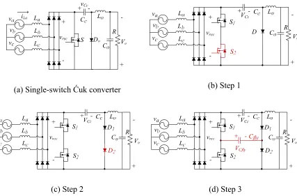
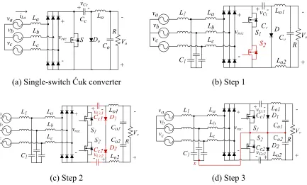
Another approach to synthesizing multilevel converters from fundamental TPSSCs is proposed here and a new family of three-phase front-end AC-DC multilevel converters can be developed. The approach is based on the connection of a neutral-point of a three-phase input capacitor filter to the general DC-DC structure and is proposed in this section. In the case of converters with capacitive input filters [Figs. 2.1(d)-(f)] such a neutral point is inherent in the converter. In the case of converters with inductive input filters [Figs. 2.1(a)-(c)], additional filtering is required to filter out high frequency harmonics so that additional input capacitors are needed and it is from these additional input capacitors that a neutral point can be created for the conversion of a single-switch topology into a multilevel neutral point topology [22]-[25].
Table 2.2: Peak switch voltage stress equations for FCMCs.
Converter Equation
Boost VS,pk = Vo/2
Ćuk VS1,pk = VCc,pk - VCfly, VS2,pk = VCfly
Sepic VS1,pk = VCc,pk + VCfly - Vo, VS2,pk = VCfly + Vo
Buck VS1,pk = Vrec,pk - VCfly = √3* VCa,pk - VCfly, VS2,pk = VCfly
Buck-boost VS1,pk = Vrec,pk + Vo - VCfly, VS2,pk = VCfly
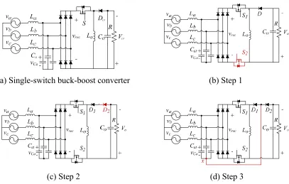
(a) Single-switch buck-boost converter
S1 R
Co
va
vb
vc
La
Lb
Lc
Ca
S2
Lo
D
+
-vCa
Vo
+
-+
vrec
-(b) Step 1
(c) Step 2 (d) Step 3
Fig 2.5: Synthesis of an example flying capacitor multilevel converter – Buck-boost FCMC.
(a) Single-switch Ćuk converter (b) Step 1
(c) Step 2 (d) Step 3
Multilevel topologies for the six fundamental converters based on the use of the neutral point of the input capacitors are shown in Fig. 2.7. For the case of the converters
with input inductor filter such as the boost, Ćuk and Sepic [Figs. 2.7(a)-(c)], it can be
seen that the artificially created neutral point (x) of the additional input capacitors is
connected to a midpoint that is created when two power switches are connected in series. For the case of the converters with capacitive filter such as the buck, buck-boost and Zeta
[Figs. 2.7(d)-(f)], it can be seen that the natural neutral point (x) of the input capacitors is
connected to a midpoint that is created when two power diodes are connected in series.
The steps that need to be taken to convert a TPSSC into a NPCMC are shown in Fig.
2.8 for a Ćuk NPCMC (example of a converter with an inductive input filter) and Fig. 2.9
for a buck-boost NPCMC (example of a converter with an capacitive input filter). The steps are as follows:
Step 1: Add a second switch in series with the main converter switch (shown as S in Figs. 2.8(a) and 2.9(a)), as shown in Figs. 2.8(b) and 2.9(b). There are now two main switches, S1 and S2.
Step 2: Add a second diode in series with the main converter diode (shown as Do in Figs. 2.8(a) and 2.9(a)), as shown in Figs. 2.8(c) and 2.9(c). There are now two
main diodes, D1 and D2. Also distribute the required capacitances, e.g. Co = Co1 +
Co2, Cc = Cc1 + Cc2, as shown in Figs. 2.8(c) and 2.9(c)
Step 3: Connect the natural neutral point of the capacitive filter converters to the mid-point of the switches and to the mid-point of the diodes as shown in Figs. 2.8(d) and 2.9(d). In case of the inductive filter converters create an artificial neutral point by adding a capacitive filter to the input and then connect that to the mid-point of the switches, the diodes and output capacitors.
For the converters shown in Figs. 2.7(a)-(c), since the switch stress is mainly
dependent on the output voltage (Vo), it can be reduced by splitting the output capacitor
(Co) so the switch stress is dependent on Vo/2. For the converters shown in Figs.
reduced by ensuring that a main power switch is exposed to line-neutral input capacitor voltages instead of line-line voltage as in Figs. 2.1(d)-(f), which results in a voltage stress
reduction by a factor of √3.
The peak voltage stresses of the switches in a NPCMC are shown in Table 2.3. It can be seen that unlike the peak voltage switch stresses shown in Table 2.2, they are evenly
Inductive Input Filter Capacitive Input Filter
(a) Boost converter (d) Buck converter
(b) Ćuk converter (e) Buck-boost converter
(c) Sepic converter (f) Zeta converter
distributed among the two switches in the converter and they are considerably less than those of a switch in a TPSSC, shown in Table 2.1.
2.6 Conclusion
Three-phase AC-DC power conversion is typically done using six-switch circuit structures. An attractive way of reducing the cost, size, and complexity of such converters for lower power applications is to use single-switch converters. The peak voltage stress of the main power switch in these converters, however, is excessive, and makes these converters impractical for most applications. It is to reduce the voltage stress of this switch that multilevel circuit structures were investigated in this chapter.
Two types of multilevel converter structures were investigated in this chapter – a family of flying capacitor multilevel converters (FCMCs) and a family of new neutral-point connected converters (NPCMCs). Since three-phase single-switch converters
(TPSSCs) are based on the basic DC-DC topologies – boost, buck, buck-boost, Ćuk,
Zeta, Sepic – and there are six such topologies, FCMCs and NPCMCs that are based on o
a
b
c o
c o
a
b
c
Cc
o La
rec
(a) Single-switch Ćuk converter (b) Step 1
(c) Step 2 (d) Step 3
each basic topology were presented. The steps needed to convert a TPSSC into its FCMC and NPCMC counterparts were presented and it was explained that the peak voltage stresses of the switches in a FCMC are generally uneven except for those of a FCMC boost converter, while the peak voltage switch stress of the switches in a NPCMC are equal and approximately half those of a switch in its counterpart TPSSC.
(a) Single-switch buck-boost converter (b) Step 1
(c) Step 2 (d) Step 3
Chapter 3
3
A Novel Three-Phase Neutral Point Connected
Buck-Boost AC-DC Converter
3.1 Introduction
In Chapter 2, two types of three-phase reduced switch multilevel converters that are based on three-phase single-switch AC-DC converter were discussed – a family of flying capacitor multilevel converters (FCMCs) and a new family of neutral point connected multilevel converters (NPCMCs). In this chapter a candidate converter, the buck-boost NPCMC [Fig. 2.5(e)], is selected as an example converter to further study the operation, properties and characteristics of the new family of NPCMCs. Other reasons for selecting this particular converter for further study are that it can step up and step down voltage (since it is a buck-boost converter). A fair amount of investigation has been done on three-phase AC-DC step-up converters with an inductive input filter and step down converters with a capacitive input filter; however, there is no literature available about step-up converters with capacitive filter. Also, the candidate converter is the simplest and thus the most practical out of the four converters that can step up and step down the
voltage, the others being the Ćuk, Sepic and Zeta converters.
In this chapter, the steady-state operation of the buck-boost NPCMC converter for both voltage step-down (buck) and voltage step-up (boost) operation is explained in detail and the converter's steady-state characteristics are determined by mathematical analysis. Based on the results of the analysis, a procedure that can be used in the design of the converter’s key components is developed and then demonstrated with an example. The feasibility of the proposed converter is confirmed with results obtained from an experimental prototype.
3.2
Operation of the Proposed Converter
The proposed buck-boost NPCMC is shown in Fig. 3.1(a). It can be seen that the input three-phase LC filter is followed by a three-phase diode bridge. On the DC side there are
output filter capacitor (Co) and resistive load R. The common point of the input capacitors
or the neutral point (x) is connected between the two output diodes.
Input power factor correction (PFC) is performed in a way similar to that of a three-phase single-switch converter with a capacitive input filter - by the appropriate charging and discharging of the input capacitors, as explained in Section 1.7.2 [33]-[35]. The
connection between x and mid-point of the diodes ensures the switch voltage stress is
limited to the peak value of the input capacitor phase voltage, which helps reduce peak voltage switch stress.
The proposed buck-boost converter steps-down the input voltage or operates as a buck
converter when its switch duty cycle, D < 0.5. The converter steps-up the input voltage or
operates as a boost converter when D > 0.5. This section describes the operation of the
proposed converter when D < 0.5 and D > 0.5. Fig. 3.1(b) indicates the reference current
and voltage directions for the most important components. The equivalent circuit
diagrams for the proposed converter steady-state operation when D < 0.5 and D > 0.5 are
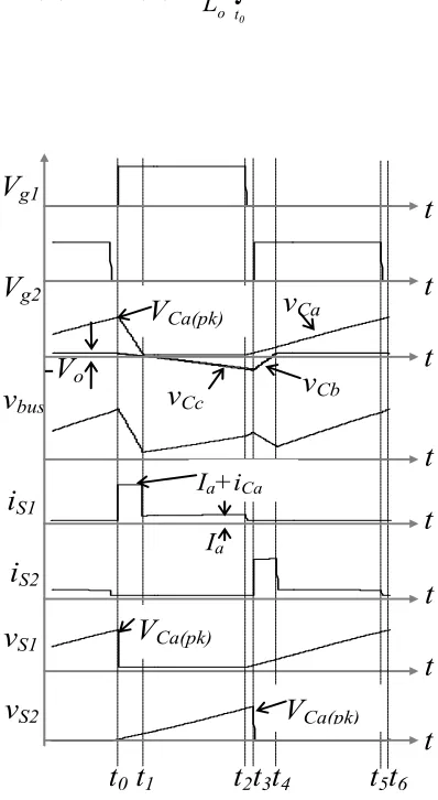
given in Figs. 3.2 and 3.4 and the typical waveforms of the two operations are given in Figs. 3.3 and 3.5 respectively.
The following assumptions are made to simplify the modal equations for the steady-state operation of the converter:
The line frequency (fl) is small with respect to the switching frequency (fs); thus the
input side voltages and currents are considered as constants during a switching
(a). Circuit diagram (b). Current and voltage reference directions.
period (Ts = 1/fs).
The input filter capacitors are considered to have equal values Ca = Cb = Cc = C.
Similarly, all three input inductors are of equal value such that La = Lb = Lc = L.
It is assumed that C is small and there is sufficient current in the DC side to
discharge the input capacitors completely during a switching cycle, throughout the line cycle so that they operate in discontinuous voltage mode (DVM) as described in Section 1.7.2.
The output capacitor Co and the load resistor R are combined and considered as a
DC voltage source (V2) and the output inductor current is considered as a DC
current ILo,k with negligible ripple.
Due to the symmetry of a three-phase system, it is sufficient to consider only π/6 of
the line cycle [31]. The equations derived below are found for a switching cycle k
in the line cycle for the interval ωlt ε [π/3, π/2] where Va,k = V1, Vb,k = Vc,k = -V1/2
and V1 being the peak phase voltage. It should be noted that the equations can be
generated by starting from any switching cycle; this particular cycle was selected to reduce redundant equations.
3.2.1
D
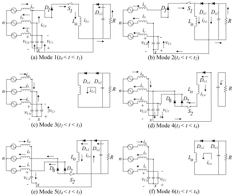
< 0.5 [Buck mode of operation]
Prior to t = t0, both S1 and S2are off and the input capacitors are charged by the input
line currents. While this is happening, the current in Lo (ILo,k) is freewheeling in the DC
side of the converter.
Mode 1 (t0 < t < t1), [Fig. 3.2(a)]:
At t = t0, S1 is turned on and the line current, Ia,k, and the discharging current of Ca
(ICa,k) flow through rectifier diode D1 and enter the DC side. Currents Ia,k and ICa,k flow
through S1, Lo, Do2 and return to the AC side. ILo,k Ia,k ICa,k. At the common point of
the input capacitors (x), the returning current splits as Ia,k and ICa,k. The voltage of the Ca
at t = t1, can be expressed as follows by considering its discharge:
a 0 1 k , a k , Lo ) 0 t ( k , Ca ) 1 t ( k ,
Ca C
t t I I V
where VCa,k,(t0) is the initial voltage or the peak value of vCa for the kth switching cycle, and Ia,k is the line current for phase A in kth switching cycle. At the input side, Ia,k further divides into Ib,k and Ic,k (Ia,k = -Ib,k - Ic,k). Ib,k and Ic,k respectively charge Cb and Cc. Cc
begins to charge from –V2 and reach voltage VCc,k(t1) at t = t1 when the mode ends, and its
voltage can be expressed as follows:
c 0 1 k , a 2 ) 1 t ( k ,Cc 2C
t t I V
V (3.2)
Mode 1 ends when Ca is fully discharged (VCa,k,(t1) = 0); thus t1 can be calculated as
follows by rearranging Eq. (1):
Lo,k a,k
) 0 t ( k , Ca a 0
1 I I
V C t
t (3.3)
Mode 2 (t1 < t < t2), [Fig. 3.2(b)]:
At t = t1, Ca becomes fully discharged and during this mode, Ca remains discharged,
line current Ia,k flows through D1 and S1,Lo and Do2. Ia,k returns to the input side and
continues to charge Cb and Cc. ILo,k freewheels through Lo, Do1, Do2 and the load.
Mode 3 (t2 < t < t3), [Fig. 3.2(c)]:
This mode begins at t = t2 when S1 is turned off. During this mode, both S1 and S2 are
off and the AC input side is separated from the DC output side. In the AC input side, the
phase currents continue to charge Cb and Cc, and Ca will begin to be charged by Ia,k.
Mode 3 ends when S2 is turned on at t = t3 (t3 = t0 + Ts/2) due to the 180o phase shift
between the two switches and the value of VCa,k at the end of the mode is
a 2 3 k , a ) 3 t ( k , Ca C t t IV (3.4)
Mode 4 (t3 < t < t4), [Fig. 3.2(d)]:
During Mode 4 Ca continues to be charged by Ia,k while Cb and Cc are discharged by
and S2. (Ib,k + ICb,k) and (Ic,k + ICc,k) return to the input side via D6 and D2 respectively.
Mode 4 ends when Cb and Cc are discharged to a voltage level of -V2 (these capacitors
charge opposite to the reference directions shown in Fig. 4(b)) at t = t4 as given below
c o Cc(t3)
Lo,k a,k
3
4 t 2C V V I I
t (3.5)
Mode 5 (t4 < t < t5), [Fig. 3.2(e)]:
During this mode, Ca continues to be charged by line current Ia,k while the voltage
across Cb and the voltage across Cc remain at -V2. Ia,k flows through Do1 while ILo,k
(a) Mode 1(t0 < t < t1) (b) Mode 2(t1 < t < t2)
(c) Mode 3(t2 < t < t3) (d) Mode 4(t3 < t < t4)
(e) Mode 5(t4 < t < t5) (f) Mode 6(t5 < t < t6)
freewheels through Lo, Do2, and the load.
Mode 6 (t5 < t < t6), [Fig. 3.2(f)]:
This mode begins when S2 is turned off at t = t5. Since both S1 and S2 are off, this mode
is similar to Mode 3. During this mode, Ca reaches its peak voltage for kth cycle while Cb
and Cc begin to charge as given below
a 3 s k , a ) 3 t ( k , Ca ) 6 t ( k , Ca C t T I VV (3.6)
c s k , a o ) 6 t ( k ,Cc 2C
T D 1 I V
V (3.7)
Mode 6 ends when S1 is turned on at t = t6 and the next switching cycle (k+1) begins.
3.2.2
D
> 0.5 [Boost mode of operation]
It should be noted that unlike in the buck mode in the boost mode, the input capacitor
discharging currents and the current of Lo are not constant during the kth switching cycle;
thus those variables are represented by lower-case letters below.
Before t = t0, S1 is off and S2 is on. Ca is charged by line current Ia,k while Cb and Cc discharge, giving currents iCc,k and iCb,k respectively.
Mode 1 (t0 < t < t1), [Fig. 3.4(a)]:
At t = t0, S1 is turned on and Ca begins to discharge; therefore Ia,k and the discharging
current of Ca (iCa,k) flow through switch S1 and charge Lo, before returning to the AC side
through switch S2, D6 and D2. The discharging current of Cb is iCb,k. The current in D6
equals Ib,k + iCb,k. The current in D2 consists of Ic,k and discharging current of Cc (iCc,k).
Both diodes Do1 and Do2 are off. This mode ends when Cb and Cc are charged in the
opposite direction to a voltage level that equals the output voltage (-V2). The voltage of