Dhonvan Srinu
1, Dhonvan Sindhu
2,Vemireddy Kalavathi
31,3
Assistant Professor in ECE dept
at Marri laxman reddy institue of technology andManagement,Dundigal,Hyderabad,Telangana, India
ABSTRACT:The major dynamic power consumers in computing and consumer electronics products is thesystem’s clock signal, typically responsible for 30%–70% of the total dynamic power consumption. Clock gatingis a predominant technique used for power saving. The Data driven clock gating is used for reduce powerconsumption in synchronous circuits .Common clock gating is used for power saving. However clock gatingstill leaves larger amount of redundant clock pulses. Multibit flip-flop is also used to reduce powerconsumption .Using of Multibit Flip-Flop method is to eliminate the total inverter number by sharing theinverters in the flip-flop .Combination of Multibit Flip-Flop with Data driven clock gating will increase thefurther power saving. Xilinx software tool and quatrus II for power analysis is used for implementing thisproposed system.
KEYWORDS-Data Driven clock gating
I. INTRODUCTION
The data of digital systems are usually stored in flip-flops (FFs),each of which has its own internal clock driver. In an attempt toreduce the clock power, several FFs can be grouped into a modulecalled a multibit FF (MBFF) that houses the clock drivers of allthe underlying FFs. We denote the grouping of kFFs into an MBFFby a k-MBFF. Kapoor et al. [1] reported a 15% reduction ofthe total dynamic power in a 90-nm processor design. Electronicdesign automation tools, such as Cadence Liberate, support MBFFcharacterization.
The benefits of MBFFs do not come for free. By sharing commondrivers, the clock slew rate is degraded, thus causing a largershort-circuit current and a longer clock-to-Q propagation delay tpCQ.To remedy this, the MBFF internal drivers can be strengthened at thecost of some extra power. It is therefore recommended to apply theMBFF at the
RTL design level to avoid the timing closure hurdlescaused by the introduction of the MBFF at the backend design stage.Due to the fact that the average data-to-clock toggling ratio of FFsis very small, which usually ranges from 0.01 to 0.1 [2], the clockpower savings always outweigh the short-circuit power penalty of thedata toggling.
An MBFF grouping should be driven by logical, structural, andFF activity considerations. While FFs grouping at the layout levelhave been studied
thoroughly, the front-end implications of
MBFFgroup size and how it affects clock gating (CG) has attracted littleattention. This brief responds to two questions. The first is what theoptimal bit multiplicity k of data-driven clock-gated (DDCG) MBFFsshould be. The second is how to maximize the power savings basedon data-to-clock toggling ratio (also termed activity and data togglingprobability).
In existing system power reduction is achieved by using clock gating. With clock gating, the Clock signals are multiply with an AND gate logic to explicitly predefined enabling signal. But this clock gating still leaves large number of redundant clock pulses. Although substantially increasing design productivity, such tools require the employment of a long chain of automatic synthesis algorithms, from register transfer level (RTL) down to gate level and net list. Unfortunately, such automation leads to a large number of unnecessary clock toggle, thus increasing the number of wasted clock pulses at flipflops (FFs) as shown in this paper through several industrial examples. Consequently, development of automatic and effective methods to reduce this inefficiency is desirable. In the sequel, we will use
the terms toggling, switching, and activity
interchangeably
II. RELATED WORN
Several dynamic power control techniques are adopted in VLSI circuits out of which the most important oneis clock gating.[5] uses multiple deliver voltages to reduce clock tree energy. The incoming, high voltage clocksignal is down-scaled through a low-voltage buffer level. The low-Vdd signal is then
propagatedthroughout the circuit, and regenerating factors (e.g., buffers) are inserted into the tree structure to make sure theappropriate pace and slew rate of the transitions. Finally, the original high-voltage is restored thru level shifters before the clock alerts feed the flip-flops.
In [3] Clock Distribution the use of Multiple Voltages reduces the rate of buffering and voltageconverters this is crucial inside the electricity discount technique implemented the use of more than one supply voltages. Themethod supplied with the aid of Pangjung and Sapatnekar addresses this predicament with the aid of providing an extra sophisticatedset of rules for introducing buffers into the clock tree and for putting the low-to-high voltage shifters, which areno longer necessarily positioned right in the front of the flip-flops. The set of rules considers the opportunity of buffer insertion after each step of backside-up subtree merging. In the diversion of keeping the skew very near zero,the set of rules guarantees that the range of regenerating factors is equalized along any root-to-sink paths ofthe tree. However, no matter the stable theoretical basis of this answer, experimental effects confirmed very smalldifferences with the clock bushes generated through the approach the usage of multiple supply voltagesIn [2] makes a specialty of Interconnect Power, i.e. Power dissipation due to the switching of interconnectioncapacitances, which can be a part of the full switched capacitance of every internet– Cj. Applying wire capacitancediscount techniques to a small percent of the wires can keep the majority of the interconnect energy.
Capacitance may be reduced by means of interconnect reduction and increasing interconnect spacing thereby decreasingcapacitance and thereby reducing electricity dissipation.
In [4], a evaluate of some current strategies to be had for clock gating is provided. Also a brand newa method that provides more immunity to the
prevailing problems in available strategies is mentioned.
III. METHOD OF SOLUTION
Multi-bit Flip-Flop method is to eliminate thetotal inverter number by sharing the inverters in
theflip-flops. Data driven clock gating reduce
redundantclock pulses. Combination of Multi-bit Flip-Flopwith Data driven clock gating will increase thefurther power saving. Xilinx software tool is used for
implementing this proposed system. This
paperstudies data-driven clock gating, employed for FFs at
the gate level, which is the most aggressive possible.The clock signal driving a FF is disabled (gated)when the FFs state is not subject to change in the next
clock cycle [7]. Data-driven gating is causing areaand power overheads that must be considered. In anattempt to reduce the overhead, it is proposed togroup several FFs to be driven by the same clocksignal, generated by bring the enabling signals of the
individual FFs. This may however, lower
thedisabling effectiveness. It is therefore beneficial
togroup FFs whose switching activities are
highlycorrelated and derive a joint enabling signal. In arecent paper, a model for data-driven gating isdeveloped based on the toggling activity of theconstituent FFs [9].
The optimal fan-out of a clockgater yielding maximal power savings is derivedbased on the average toggling statistics of theindividual FFs, process technology, and cell library inuse. In general, the state transitions of FFs in digitalsystems depend on the data they process. Assessingthe effectiveness of data-driven clock gating requires,therefore, extensive simulations and statisticalanalysis of the FFs’ activity. Another grouping of FFs
ofindividual FFs, while grouping for data-driven clockgating should combine toggling similarity withphysical position considerations. While [9] answered
the question of what is the group size that maximizes power savings, this paper studies the questions of: 1)which FFs should be placed in a group to maximizethe power reduction and 2) how to algorithmicallyderive those groups.
Data-Driven Clock Gating
Clock enabling signals are very well understood atthe system level and thus can effectively be definedand capture the periods where functional blocks and modules do not need to be clocked. Those are laterbeing automatically synthesized into clock enabling
signals at the gate level. In many cases, clockenabling signals are manually added for every FF as a
part of a design methodology. Still, when modules ata high and gate level are clocked, the state transitions
of their underlying FFs depend on the data beingprocessed. It is important to note that the entiredynamic power consumed by a system stems fromthe periods where modules’ clock signals
areenabled. Therefore, regardless of how
relativelysmall this period is, assessing the
effectiveness ofclock gating requires extensive simulations andstatistical analysis of FFs toggling activity, aspresented subsequently.
Fig. 1 Practical data-driven clock gating
Let the average toggling probability of a FF (alsocalled activity factor) be denoted by p (0 <p< 1).Under the worst-case assumption of independent FFtoggling, and assuming a uniform physical clock
treestructure, it is shown in [9] that the number k ofjointly gated FFs for which the power savings aremaximized is the solution of
(1− p)kln(1− p) (cFF+cW) +clatch/ k2=0 ……… (1)
Where cFF is the FFs clock input capacitance, cW is the unit-size wire capacitance, and clatch is the latch capacitance including the wire capacitance of its clkinput. Table I shows how the optimal k depends on p.
Such a gating scheme has considerable
timingimplications, which are discussed in [9]. We
willreturn to those when discussing the
implementationof data-driven gating as a part of a complete designflow.
Implementation and Integration Ina Design Flow:
In the following, we describe the implementationof
data-driven clock gating as a part of a
standardbackend design flow. It consists of the followingsteps.
1) Estimating the FFs toggling probabilitiesinvolves running an extensive test benchrepresenting typical operation modes of thesystem to determine the size k of a gated FFgroup by solving (1).
2) Running the placement tool in hand to getpreliminary preferred locations of FFs in thelayout.
3) Employing a FFs grouping tool to implementthe model and algorithms presented, using the toggling correlation dataobtained in Step 1 and FF locations’ dataobtained in Step 2. The outcome of this step isk-size FF sets (with manual overrides ifrequired), where the FFs in each set will bejointly clocked by a common gater.
ondesign methodology in use and its discussion isbeyond the scope of this paper. We have
introduced the gating logic into the RTLdescription.
5) Re-running the test bench of Step 1 to verifythe full identity of FFs’ outputs before and afterthe introduction of gating logic. Although datadriven gating, by its very definition, should notchange the logic of signals, and hence FFstoggling should stay identical, a robust designflow must implement this step.
6) Ordinary backend flow completion. From thispoint, the backend design flow proceeds byapplying ordinary place and route tools. This isfollowed by running clock-tree synthesis.
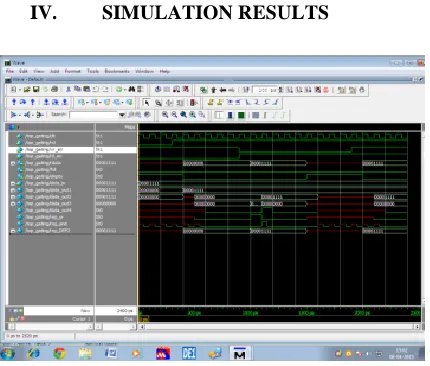
IV. SIMULATION RESULTS
Fig. 2 Output Waveform of Clock GatedSynchronous FIFO
Fig. 3 Output Wave form of Synchronous FIFO Using MultibitFlipflopWith Data Driven Clock
Gating.
V. CONCLUSION
Common clock gating is used forpower saving. But clock gating still leaves largeramount of redundant clock pulses. Multibit flip-flopis also used to decrease power consumption. Using ofMultibit Flip-Flop method is to remove the totalinverter number by sharing the inverters in the flipflops. Combination of Multibit Flip-Flop with Datadriven clock gating will increase the additional powersaving. Xilinx software tool is used for implementingthis proposed system. The combination of data-drivengating with MBFF in an attempt to yield additionalpower savings.
REFERENCES
[1] A. Kapoor et al., “Digital systems power management for high performance mixed signal platforms,” IEEE Trans. Circuits Syst. I, Reg.Papers, vol. 61, no. 4, pp. 961–975, Apr. 2014.
[2] H. Zhang, J. Rabaey, ―Low-Swing Interconnect
Interface Circuit”s,ISLPED-98: ACM/IEEE
International Symposium on LowPower Electronics and Design, pp. 161-166, Monterey, CA, August 1998.
[3] J. Pangjun, S. S. Sapatnekar, ―Clock Distribution using Multiple Voltages, ISLPED-99: ACM/IEEE International Symposium onLow-Power Electronics and Design, pp. 145-150, San Diego, CA, August 1999.
[4] JagritKathuria,M. Ayoubkhan ,Arti Noor. ”A R e v i e w o f C l o c k Ga t i n g Tech n iq u e s ”, MIT
International Journal of Electronics and
CommunicationEngineering Vol. 1 No. 2 Aug 2011 pp 106-114.
[5] L. Benini, A. Bogliolo, and G. De Micheli, ―A survey on design techniques for system-level dynamic power management, IEEETrans. Very Large Scale Integr. (VLSI) Syst., vol. 8, no. 3, pp. 299–316, Jun. 2000.
[7]. C. Chunhong , K. Changjun and S.Majid "Activity-sensitive clock treeconstruction for low power", Proc. Int.Symp.Low Power Electron. Design, pp.279 -2822002
[8]. G. Palumbo , F. Pappalardo and S.Sannella "Evaluation on power reductionapplying gated clock approach", Proc. IEEEISCAS 2002, vol. 44, pp.IV85 -IV88 2002
[9]. M. E. Hamid and C. H. Chen "A note to lowpower linear feedback shift register", IEEETrans. Circuits Syst. II, Analog Digit. SignalProcess., vol. 45, no. 9, pp.1304 -13071998
[10]. T. Lang , E. Musoll and J.Cortadella "Individual flip-flops with gatedclocks for low power datapaths", IEEETrans. Circuits Syst. II, Analog Digit. SignalProcess., vol. 44, no. 6, pp.507 -516 1997
[11]. M. Lowy "Parallel implementation of
linearfeedback shift register for low
powerapplications", IEEE Trans. Circuits Syst. II,Analog Digit. Signal Process., vol. 43, no.6, 1996.
[12] S.-H. Wang, Y.-Y.Liang, T.-Y.Kuo, and W.-K.
Mak, “Power-driven flipflop merging and
relocation,” IEEE Trans. CAD Integr. Circuits Syst.,vol. 31, no. 2, pp. 180–191, Feb. 2012.
[13] S-C. Lo, C-C. Hsu, and MP-H. Lin, “Power optimization for clocknetwork with clock gate cloning and flip-flop merging,” in Proc. ACMInt. Symp. Phys. Design, 2014, pp. 77–84.
[14] S. Wimer, D. Gluzer, and U. Wimer, “Using well-solvable minimumcost exact covering for VLSI clock energy minimization,” OperationsRes. Lett., vol. 42, no. 5, pp. 332–336, Jul. 2014.
[15] SpyGlass Power, accessed on 2016. [Online]. Available:http://www.atrenta.com /solutions/spyglass-family/spyglass-power.htm
BIODATA
AUTHOR1
Dhonvan Srinu received his B.Tech in ECE ( Electronic and communication Engineering).at Vaagdevi College of Engineering , Warangal dist. Telangana. And P.G received in ECE (DECS)in VLSI System Design. Aurora College of Engineering , Nalgonda..Dist. Telangana, India. He is currently working as a assistant professor in ECE dept at Marri laxman reddy institue of technology and Management dundigal, Hyderabad ,Telangana, India. She has 7 years of teaching experience.
AUTHOR2
Dhonvan Sindhu received her B.Tech in ECE in Kodada Onstitute of Technology and Science for women.Kodada. And P.G received in ECE (Embedded Systems) in Aravindaksha Educational Society’s Group of Institutions,Balemla,Suryapeta,SuryapetaDist. Telangana, India.
AUTHOR3