A Frequency Band Reconfigurable UWB Antenna
for High Gain Applications
Ritesh K. Saraswat1, * and Mithilesh Kumar2
Abstract—An octagonal shape patch antenna with switchable inverted L-shaped slotted ground is designed for frequency band reconfigurable and experimentally validated. The antenna is capable of frequency band switching at five different states including an ultra wideband (UWB) state, two narrowband states and a dual-band state by using RF switching element p-i-n diodes. In the case of ultrawide band (UWB) state, the proposed antenna operates over impedance bandwidth of 141% (2.87– 16.56 GHz) under simulation and 139% (2.85–15.85 GHz) in measurement with return lossS11<−10 dB. For two narrowband states, 10 dB impedance bandwidth achieved is 16% (5.05–5.91 GHz) and 11% (8.76–9.80 GHz) under simulation and 14% (5.01–5.79 GHz) and 10% (8.68–9.69 GHz) in measurement, respectively. For the dual band state, 10 dB impedance bandwidth of 2.21–2.52 GHz (13%) & 5.07– 5.89 GHz (15%) and 2.18–2.52 GHz (14%) & 8.78–9.71 GHz (10%) under simulation and 2.20–2.50 GHz (12%) & 5.05–5.90 GHz (15%) and 2.19–2.50 GHz (13%) & 8.70–9.60 GHz (9%) in measurement with return lossS11<−10 dB. The proposed antenna is capable to serve in different wireless communication applications such as WLAN [802.11b/g/n (2.4–2.48 GHz), 802.11a/h/j/n (5.2 GHz), ISM band (2.4– 2.5 GHz)], Bluetooth (2400–2484 MHz), WiMAX (2.3–2.4 & 5.15–5.85 GHz), WiFi (2.40–2.48, 5.15– 5.85 GHz) and UWB (3.1–10.6 GHz). It also works at 9.2 GHz where airborne radar applications are found. Next, the antenna gain is improved with the help of a circular loop frequency selective surface (FSS) and a PEC (perfect electric conductor) sheet. Measured peak gain represents average improvements about 4 dB–5 dB over the UWB band. Experimental results seem in good agreement with the simulated ones of the proposed antenna with and without the frequency selective surface.
1. INTRODUCTION
In recent years, due to rapid development in the field of wireless communications, the demand with mobile devices operating under different standards or applications is extending. The wireless systems are evolving in the direction of multi-functionality. For multi-functionality, antenna parameters such as operating frequency, radiation pattern, impedance bandwidth and polarization are reconfigured in order to fulfill the current or future demand [1]. Cognitive radio system is one of the future wireless communication systems, where a sensing antenna with the capability of monitoring the spectrum is required, and that can be reconfigured to communicate over a chosen frequency band. In this system, a frequency reconfigurable antenna is required either for spectrum sensing or communication [2]. Most of the frequency-reconfigurable antennas are capable to operate only for narrowband switching modes [3– 5]. A switchable quad-band antenna has been proposed by using microelectromechanical systems (MEMS) switch [3]. The microstrip patch antenna can operate in four different frequency modes by controlling the states of switches [4]. Recently, a number of frequency band reconfigurable antennas have been designed, which combine the narrowband and wideband functionalities [6–11]. In [6], a Vivaldi
Received 1 September 2015, Accepted 3 November 2015, Scheduled 6 November 2015
* Corresponding author: Ritesh Kumar Saraswat (ritesh.saraswat9@gmail.com).
1 M.L.V. Govt. Textile & Engineering College, Bhilwara (Rajasthan), India. 2 Rajasthan Technical University, Kota (Rajasthan),
antenna design has been proposed, providing the wideband mode and narrowband mode switching. A frequency band reconfigurable antenna with switching between an ultrawideband (UWB) mode and three narrowband modes has been designed, by using four photoconductive switches [7]. In [9], two reconfigurable monopole antennas are proposed, which provide the combination of narrowband and wideband functionalities, where the first one uses p-i-n diode switches, and the second uses varactor diodes for switching operation. The Field-Effect-Transistor (FET) active switching devices are used in different types of tunable EBG structures where the FET switches are modeled as ideal conductors for determining the transmission of the structure [12]. By changing the electromagnetic bandgaps (EBGs), the bandstop behavior of multistate periodic microwave circuit with very wide stopbands is observed for different states [13].
In this paper, we propose a novel frequency-band reconfigurable antenna with switching facility among UWB, narrowband and dual-band modes. The proposed antenna has five different switchable states: 2.87–16.56 GHz in UWB mode; 5.05–5.91, and 8.76–9.80 GHz in narrowband mode; 2.21– 2.52 GHz & 5.07–5.89 GHz and 2.18–2.52 GHz & 8.78–9.71 GHz in dual-band mode. The proposed antenna uses a switchable slotted ground structure for reconfigurability and has a simple structure and the smallest size in comparison to antennas reported in literature [6–11]. To improve the gain of the antenna, a circular loop frequency selective surface is designed and implemented. The FSS is placed beneath the antenna to act as a reflector [14]. The average gain improvement with the FSS antenna combination is around 4 dB. The CST Microwave Studio (CST MWS) software [16] is used for simulation while the measurements are taken using a E5071C (300 kHz–20 GHz) ENA series Agilent Technologies Vector Network Analyzer. The antenna and FSS structure are fabricated with the help of PCB prototype machine Caddo-71. In the following section, the antenna geometry is described in frequency band reconfigurable modes with simulated and measured results. Thereafter, the circular loop FSS and PEC sheet design is described, and the enhancements in the gain and the radiation patterns are discussed. Finally, conclusions are made.
2. ULTRAWIDEBAND (UWB) ANTENNA DESIGN
An octagonal shape monopole antenna is chosen as a basic structure to operate over wide bandwidth and has good radiation characteristics. The configuration of the proposed UWB monopole antenna is shown in Figure 1. The antenna is constructed on a Roger RT 5880 substrate with relative permittivity 2.2 and thickness 0.40 mm. The size of the substrate is 40 ×40 mm2. The radiating element is a octagonal shape patch with dimensions ab = ef = 10 mm, bc = ha = 5.14 mm, cd = gh = 6.0 mm and de=f g= 5.14 mm, which is fed with a 50 ohm microstrip feed line with length 22 mm and width 1.25 mm. On the bottom of the substrate, there is a ground plane with 21.1×40 mm2 dimensions and height 0.01 mm, below the microstrip feed line.
As per the parametric study of the proposed antenna, variation in the antenna performance with
(a) (b)
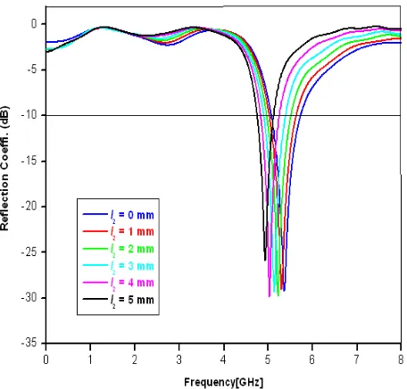
Figure 2. Simulated reflection coefficient S11 of the proposed antenna for different values ofl1.
Figure 3. Simulated reflection coefficient S11 of the proposed antenna for different values ofW1.
change in length l1 and width W1 of the ground slot is shown in Figures 2–3. As seen, by varying the slot dimensions (lengthl1 from 0 to 7 mm and widthW1 from 0.6 to 1.4 mm), the impedance matching with UWB is achieved at length l1= 6.1 mm and widthW1= 1 mm.
It is also observed from Figures 2 and 3 that the impedance matching is improved at lower frequencies (2–4 GHz) when the slot dimensions are reduced (either by reducing l1 or W1) whereas at higher frequencies (above 5 GHz) it is improved when the slot dimensions are increased.
At the optimized value ofl1= 6.1 mm andW1 = 1 mm, the input reflection coefficientS11 of UWB antenna is below −10 dB with impedance bandwidth of 141% (2.87–16.56 GHz) under simulation and 139% (2.85–15.85 GHz) in measurement, shown in Figure 4.
3. NARROWBAND AND DUALBAND ANTENNA DESIGN
The UWB monopole antenna can be reconfigured to other frequency bands by using a inverted L and rectangular-shaped slotted structure placed on the ground plane, as shown in Figure 5. This inverted
Figure 4. Simulated and measured reflection coefficientS11 of the UWB antenna.
L-slotted structure acts as a filter, which is designed to suppress the frequencies outside the desired frequency band. This embedded slot below the feed line is responsible for stopbands in the UWB range and provides a passband between them [9]. This created passband can be controlled by varying the length and shape of respective slot, as shown in Figure 6.
Figure 7 shows the input reflection coefficient S11 of the antenna below −10 dB for different filter structures. Structures I and II create dual bands whereas structures III and IV are responsible for obtaining the single bands only.
Figure 6. Filter structures placed on the ground plane.
Figure 7. Simulated reflection coefficient S11 of the antenna for filter structures in Figure 6.
Figure 8. Simulated reflection coefficient S11 of the antenna for different values ofl2 in structure-III.
Moreover, the bandwidth of each filtering structure in Figure 7 is controllable with changing the lengthl2and widthW2of parallel vertical arms (in Figure 5). By the variations of these arms dimensions, impedance bandwidth changes accordingly, as shown in Figures 8–9. By increasing the slot lengthl2and widthW2, bandwidth of the antenna decreases from 30% to 12% in structure III. Finally, the variations in the impedance bandwidth with changes in the slot dimensions indicate the presence of optimal values for the best performance.
4. RECONFIGURABLE ANTENNA DESIGN
This section is devoted to discussion on the design of an antenna which is capable of reconfiguration from UWB to two narrowband and two dual-band modes by using the filter structure on ground plane and inserting five p-i-n diode switches inside it, as shown in Figure 10. By changing effective length of the slot, different resonant frequency bands can be produced. The switches D1–D5 are positioned in such a way to obtain the required structures I–IV for desired frequency bands. If diode D1 is on and remaining ones are off, we will get a filter structure like structure-I for dual-band.
For switching operation of p-i-n diodes, we apply dc voltage by using metal strips dimension of 2×0.6 mm2 inside the main slot, as shown in Figure 10. A 100-pF dc blocking capacitor is also present in the slot, for each p-i-n diode, to provide the RF connection of the p-i-n diode as well as to isolate the RF signal from the dc. In the proposed design, ALPHA-6355 beam lead p-i-n diodes with extremely low capacitance are used [15]. For biasing of p-i-n diodes, a 0.7 V dc voltage is applied to metal strips. The ALPHA-6355 beam lead p-i-n diode exhibits an ohmic resistance of 2.6 ohm and a capacitance of 0.081 pF in the ON (forward bias) and OFF states (reverse bias), respectively. When the diodes are turned on, the metal strips are connected to the ground plane and become a part thereof.
The desired frequency band can be obtained by changing the states of five p-i-n diodes, as per Table 1. The RF equivalent circuit of the p-i-n diode is shown in Figure 11. In the case of ON-state (forward bias), the p-i-n diode works as a current-controlled resistor (Rs) connected in series with a fixed inductor (Ls). In OFF-state (reverse bias) of p-i-n diode, the equivalent circuit shows a shunt combination of the intrinsic-layer capacitance (Cp) and the parallel resistance (Rs) in series with the fixed inductance (Ls). The depleted intrinsic layer consist capacitive reactance Cp and the shunt resistance Rs. The reactive capacitance Cp contains the stray capacitanceCs due to the effects of the diode’s package structure and the junction’s capacitance Cj.
Figure 10. Switchable filter structure on the ground plane (unit: millimeters).
(a) (b)
Table 1. Details of combinations of p-i-n diodes with simulated and measured frequency band and bandwidth in each states.
Diode→
D1 D2 D3 D4 D5 Frequency Bands (in GHz) 10-dB bandwidth (%) Characteristics
States↓ Simulated Measured Simulated Measured
I ON OFF OFF ON OFF 5.05–5.91 5.01–5.79 16 14 Narrow
Band
II OFF ON OFF OFF ON 8.76–9.80 8.68–9.69 11 10 Narrow
Band
III ON OFF OFF OFF OFF 2.21–2.52
& 5.07–5.89
2.20–2.50
& 5.05–5.90 13 & 15 12 & 15
Dual Band
IV OFF ON OFF OFF OFF 2.18–2.52
& 8.78–9.71
2.19–2.50
& 8.70–9.60 14 & 10 13 & 9
Dual Band
V ON ON ON ON ON 2.87–16.56 2.85–15.85 141 139 UWB
(a) (b)
Figure 12. Images of the fabricated antenna: (a) top view; (b) bottom view.
Figure 13. Images of measurement setup for proposed antenna.
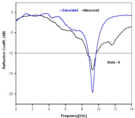
The proposed antenna is initially simulated on CST Microwave Studio (MWS) software [16] and then fabricated with the optimized dimensions, as shown in Figure 12. As per Table 1, the five operating states are investigated, and their corresponding diodes states with comparison of the simulated and measured results of frequency bands and impedance bandwidth. With respect to all the five states, the measured and simulated reflection coefficientsS11 are compared as shown in Figures 14–18 which seem to be in good agreement. As per Table 1, for States I and II two narrowband states, 10 dB impedance bandwidth achieved is 16% (5.05–5.91 GHz) and 11% (8.76–9.80 GHz) under simulation whereas 14% (5.01–5.79 GHz) and 10% (8.68–9.69 GHz) in measurement respectively. For States III and IV, the antenna operates in dual bands, impedance bandwidth of 13% (2.21–2.52 GHz) & 15% (5.07–5.89 GHz) and 14% (2.18–2.52 GHz) & 10% (8.78–9.71 GHz) under simulation and 12% (2.20–2.50 GHz) & 15% (5.05–5.90 GHz) and 13% (2.19–2.50 GHz) & 9% (8.70–9.60 GHz) in measurement respectively. For UWB state, the antenna operates over impedance bandwidth of 141% (2.87–16.56 GHz) under simulation and 139% (2.85–15.85 GHz) in measurement with return lossS11<−10 dB.
Figure 13 shows the measurement setup for proposed antenna to obtain the measured reflection coefficient by using vector network analyzer (VNA) and radiation characteristics with the help of anechoic chamber.
Figure 14. Simulated and measured reflection coefficientS11of the proposed antenna for State-I (from Table 1).
Figure 15. Simulated and measured reflection coefficientS11of the proposed antenna for State-II (from Table 1).
Figure 16. Simulated and measured reflection coefficient S11 of the proposed antenna for State-III (from Table 1).
Figure 17. Simulated reflection coefficientS11of the proposed antenna for State-IV (from Table 1).
Figure 18. Simulated and measured reflection coefficient S11 of the proposed antenna for State-V (from Table 1).
Figure 19. Surface current distribution of the proposed antenna for different frequencies.
Figure 20. Simulated gain (dB) of the proposed antenna for different frequencies.
(a) (b)
Figure 21. Measured gain of the proposed antenna for different switching states: (a) single-band and dual-band modes, (b) UWB.
(a) (b)
Figure 22. Simulated radiation efficiency of the proposed antenna for different switching states: (a) single-band and dual-band modes, (b) UWB.
reference level of 4 dB whereas at higher frequencies (above 6 GHz), the gain is improved with respect to the reference level. The antenna has an acceptable gain in narrowband and dual-band modes and a reasonably flat gain with an average of 3.9 dB in UWB mode.
Figure 23. Simulated and Measured AR (axial ratio) (along θ= 78◦ and Φ =−89◦) of the proposed antenna.
The axial ratio (AR) of the proposed antenna is measured with the help of Antenna Measurement System in conjunction with a Vector Network Analyzer inside an anechoic chamber. For obtaining the best performance regarding maximum ARBW (Axial ratio bandwidth) as shown in Figure 23, the measurement system is set up along the directions of θ = 78◦ and Φ = −89◦. The simulated AR stays less than 3 dB from 4.4–6.9 GHz which represents an ARBW of 44% centered at 5.65 GHz. The measured ARBW (axial ratio bandwidth) is slightly less than the simulated ARBW at 38% (4.65– 6.85 GHz) as shown in Figure 23. The wideband CP is achieved by optimizing the inverted L-shaped slot and rectangular slit on ground plane. Inverted L-shaped slot on the ground plane creates alternate current paths that produces two orthogonal degenerate modes on the top patch whereas the CP behavior can be enhanced by creating rectangular slits in ground plane.
5. CIRCULAR LOOP FSS DESIGN FOR GAIN ENHANCEMENT
An FSS of 8×8 circular loop is designed to improve the gain of the proposed antenna. The FSS is formed by a metallic PEC sheet with circular loop of diameter D = 7 mm on both sides of an FR4 substrate of relative permittivity εr = 4.4 and thickness 1.6 mm. A schematic of the FSS is shown in Figure 24.
The circular loop of diameter 7 mm is considered as a square loop of side length 6.2 mm [17]. The relation between the area of square loop and area of circular loop is shown in Equation (1).
l×l=πr2, (1)
where, lis the side length of square loop and r the radius of circular loop.
As per Figure 25 and Equation (1), circular loop unit cell dimension (du) is corresponding to twice of the side length of the square loop.
As shown in Figure 24, circular loop type FSS combines the characteristics of the patch type FSS and slot type FSS and is chosen for its broad band operation. In the comparison of the transmittance with a single layer circular loop FSS to a double layer circular loop FSS in Figures 26 and 27, it is easily seen that a wider bandwidth of 6.7 GHz (3.5–10.2 GHz) is achieved in the case of the latter. The impedance bandwidth so obtained is near UWB bandwidth 7.5 GHz (3.1–10.6 GHz).
Equations (2) & (3) [19, 20].
ωL = (du/p)F(p,2wm, λ) (2)
ωC = 4εr(du/p)F(p, ga, λ) (3)
where, F(p,2wm, λ) = (p/λ)[ln{cosec(π·2wm/2p) +G(p, wm, λ)}] and F(p, ga, λ) = (p/λ)[ln{cosec(π· ga/2p) +G(p, ga, λ)}].
The characteristics of the proposed circular loop FSS are measured in an anechoic chamber. For measurement, two double ridge horn antennas are used as reference antennas. Figure 29 shows the block diagram of the used measurement setup. The proposed FSS is placed between the two horn antennas (reference antennas) so that it is in the far-field region of both the antennas. The FSS is illuminated by the plane waves generated by the transmitting horn antenna at the transmitter section, and the transmitted waves through the FSS are collected by the receiving horn antenna at the receiver section. The ratio of received signal strength to transmitted signal strength (S21) is calculated using Vector Network Analyzer (VNA).
From Equations (2) and (3),ωLis the inductive reactance associated with inductanceL, andωC is the capacitive susceptance associated with capacitanceC. Gis the correction factor for the associated
Figure 24. Schematic of the proposed FSS with dimensions of the unit cell and periodicity.
Figure 25. Schematic diagram for equating the area of square loop with circular loop.
Figure 26. Simulated and measured transmis-sion (in dB) for the circular loop FSS for single layer.
inductance and capacitance and can cause minor deviation in the results if it is ignored in the present calculations. The admittance of the shunt branch representing the FSS may be expressed as,
Y ={jωL+ (1/jωC)}−1 (4)
and the magnitude of the transmission coefficient |τ| for a single FSS layer is obtained by,
|τ|2 =4/4 +|Y|2 (5)
The resonance frequency can be determined by applying the condition,
ωL= (1/ωC) (6)
For a circular loop FSS layer with dimensions as given in Table 2 and withεr = 2.7 (the mean of air and FR4), the calculated value of inductive reactanceωLis 10.3537λ−1, and capacitive susceptance
ωC is 347.3714λ−1. With these values of ωLandωC and with the help of Equation (6), the calculated resonance comes out to be 5.01 GHz. Also, the transmission coefficient magnitude|τ|is calculated by using Equations (4) and (5).
Table 2. Dimensions of the circular loop FSS.
Parameter Value (in mm) Periodicity (p) 10.5
Gap (ga) 0.5
Width of metallic loop (wm) 1.5 Dimension of the unit cell (du) 12.4
The size of FSS layer and distance from the antenna are optimized as per Tables 3(a) & (b), respectively.
The distance from the antenna at which the proposed FSS is to be placed is also decided from the reflection phase behavior. The distance should allow for constructive interference between the radiation from antenna and the reflected radiation from the FSS screen. In order to meet the requirement, we use a simple expression which can be written as given in Equation (7).
ΦFSS−2βhd= 2nπ (7)
where, n=. . . ,−2,−1,0,1,2, . . . ..
ΦFSS is the reflection phase of the FSS screen, hd the distance at which the FSS is to be placed from antenna, and β the propagation constant of free space given by 2π/λ. If we choose the reflection phase ΦFSS to be 0◦, the optimal height can be shown to behd=λ/2. Hence, the optimal height (hd) can be taken equal to half the wave-length (λ/2) at that frequency where the reflection phase of the
Figure 28. Equivalent circuit for the circular loop FSS.
Table 3. Size and distance optimization for FSS.
(a) Size optimization for the FSS.
Size of FSS Sheet (in mm2) Distance of FSS from
antenna Structure (in mm) Peak Gain (in dB)
40×40 20 5.47
60×60 20 6.7
80×80 20 8.31
83.5×83.5 20 8.57
100×100 20 8.47
120×120 20 8.53
(b) Distance optimization for the FSS.
Size of FSS Sheet (in mm2) Distance of FSS from
antenna Structure (in mm) Peak Gain (in dB)
83.5×83.5 05 7.76
83.5×83.5 10 8.24
83.5×83.5 15 8.29
83.5×83.5 20 8.57
83.5×83.5 25 8.26
83.5×83.5 30 7.45
(a) (b)
Figure 30. (a) Image of proposed FSS without structure (side view), (b) image of proposed FSS with structure (top view).
FSS (ΦFSS) is zero. For the designed circular loop FSS, the frequency at which the reflection phase is 0◦ is found to be 7.51 GHz. Hence, the optimal height is calculated as 20 mm. In Figure 30, an image of the circular loop FSS screen is shown while the antenna along with the FSS screen is mounted at optimal height of 20 mm.
A comparison of simulated and measured reflection coefficients (S11) of the antenna without the FSS and with the circular loop FSS are shown in Figure 31. It can be seen from Figure 31 that the impedance bandwidth more or less remains the same after the application of the FSS screen. The impedance matching slightly deteriorates in the presence of the FSS due to induced current from reflected radiation with varying phase at other frequencies.
quasi-Figure 31. Comparison of simulated and measured reflection coefficients without and with the FSS.
Figure 32. Measured and simulated radiation patterns (antenna with and without FSS).
omnidirectional in nature whereas theH-plane radiation patterns resemble dumbbell shape. There is a good agreement seen between the measured and simulated radiation patterns for E andH planes with the slight difference caused by assembly misalignments.
Figure 33. Image of structure with PEC sheet (Top view).
Figure 34. Measured peak gains of the proposed antenna without and with the FSS and PEC sheet.
Figure 35. Simulated radiation efficiency of the proposed antenna without and with the FSS and PEC sheet.
Figure 33 shows an image of the proposed structure with PEC sheet where the antenna along with the sheet is mounted at optimal height of 20 mm.
Figure 36. Simulated and measured axial ratio (along θ = 78◦ and Φ = −89◦) of the proposed antenna with the FSS.
Figure 37. Simulated and measured axial ratio (along θ = 78◦ and Φ = −89◦) of the proposed antenna without and with the FSS and PEC sheet.
higher frequency range (above 9.0 GHz).
The simulated radiation efficiencies of the antenna with and without FSS and PEC sheet are shown in Figure 35. There is approximately a 10–15% reduction in the radiation efficiency in the case of the antenna with FSS and PEC sheet. This reduction is due to the additional losses taking place in the FSS screen or PES sheet and the substrate. It is seen from Figure 35, the radiation efficiency stays above 75% in the operating band.
The CP performance of the proposed antenna is affected in the case with the presence of FSS. It is seen in Figure 36 that the ARBW (axial ratio bandwidth) of the proposed antenna is reduced in the presence of FSS compared to the case without FSS. This effect is due to the phase change in the electric field components induced during reflection from the proposed FSS and interference between the forward traveling and reflected waves. The simulated ARBW is 36% (4.6–6.61 GHz) centered at 5.61 GHz whereas measured ARBW is 27% (4.95–6.51 GHz) centered at 5.73 GHz.
In another case, a PEC sheet is placed as a reflector below the proposed antenna and investigated. In this case, the impedance matching gets affected, and the axial ratio is disturbed by which ARBW (axial ratio bandwidth) is observed to be reduced as shown in Figure 37.
6. CONCLUSION
A novel band-reconfigurable octagonal shape monopole antenna with completely switchable frequency bands has been presented. The antenna uses switchable slotted structure on the ground plane to provide band-reconfigurable capability. The proposed antenna is simple to design and uses five p-i-n diodes to switch on the desired frequency bands. The proposed frequency-band reconfigurable antenna is intended for the use in cognitive radio and multi-radio wireless applications.
REFERENCES
1. Zhang, C., S. Yang, H. K. Pan, A. E. Fathy, and V. K. Nair, “Frequency reconfigurable antennas for multi radio wireless platforms,”IEEE Microwave Magazine, Vol. 10, No. 1, 66–83, Feb. 2009. 2. FCC (Federal Communications Commission), First Report and Order, Feb. 14, 2002.
3. Li, R. L., T. Wu, S. Y. Eom, S. S. Myoung, K. Lim, J. Laskar, S. I. Jeon, and M. M. Tentzeris, “Switchable quad-band antennas for cognitive radio base station applications,” IEEE Trans. Antennas Propagation, Vol. 58, No. 5, 1468–1476, May 2010.
4. Mahmoud, S. F. and A. F. Sheta, “A widely tunable compact patch antenna,” IEEE Antennas Wireless Propagation Letter, Vol. 7, 40–42, 2008.
5. Huang, C. T. and T. Y. Han, “Reconfigurable monopolar patch antenna,” Electron Lett., Vol. 46, No. 3, 199–200, Feb. 2010.
6. Gardner, P., M. R. Hamid, P. S. Hall, and F. Ghanem, “Switched-band Vivaldi antenna,” IEEE Trans. Antennas Propagation, Vol. 59, No. 5, 1472–1480, May 2011.
7. Li, R. L., G. P. Jin, and D. L. Zhang, “Optically controlled reconfigurable antenna for cognitive radio applications,” Electron Lett., Vol. 47, No. 17, 948–950, Aug. 2011.
8. Gardner, P., M. R. Hamid, P. S. Hall, and F. Ghanem, “Vivaldi antenna with integrated switchable band pass resonator,” IEEE Trans. Antennas Propagation, Vol. 59, No. 11, 4008–4015, Nov. 2011. 9. Ghafouri-Shiraz, H. and A. Tariq, “Frequency-reconfigurable monopole antennas,” IEEE Trans.
Antennas Propagation, Vol. 60, No. 1, 44–50, Jan. 2012.
10. Gardner, P., J. R. Kelly, and P. S. Hall, “Integrated wide-narrow band antenna for switched operation,” Processing IEEE EuCAP, 3757–3760, Berlin, Germany, 2009.
11. Boudaghi, H., M. Azarmanesh, and M. Mehranpour, “A frequency-reconfigurable monopole antenna using switchable slotted ground structure,” IEEE Antennas and Wireless Propagation Letters, Vol. 11, 2012.
12. Dushmantha, N., P. Thalakotuna, L. Matekovits, M. Heimlich, K. P. Esselle, and S. G. Hay, “Active switching devices in a tunable EBG structure: Placement strategies and modeling,” Journal of Electromagnetic Waves and Applications, Vol. 25, Nos. 11–12, 1740–1751, 2011.
13. Dushmantha, N., P. Thalakotuna, K. P. Esselle, L. Matekovits, M. Heimlich, and S. G. Hay, “Changing the electromagnetic bandgap and stopbands in a multistate periodic circuit,”Microwave and Optical Technology Letters (MOTL), Vol. 55, No. 8, 1871–1874, Aug. 2013.
14. Kushwaha, N. and R. Kumar, “Design of slotted ground hexagonal microstrip patch antenna and gain improvement with FSS screen,” Progress In Electromagnetics Research B, Vol. 51, 177–199, 2013.
15. Alpha Industries, “ALPHA-6355 beamlead PIN diode,” Data sheet, [Online]. Available: http://www.datasheetarchive.com/ALPHA/PIN diode 6355-datasheet.html.
16. Computer Simulation Technology — CST (Microwave Studio MWS), Version-2014.
17. Ray, K. P. and G. Kumar, “Determination of resonant frequency of microstrip antennas,”Microw. Opt. Technol. Lett., Vol. 23, 114–117, 1999.
18. Langley, R. J. and E. A. Parker, “Equivalent-circuit model for arrays of square loops,” Electron Lett., Vol. 18, 294–296, 1982.
19. Chung, Y.-C., K.-W. Lee, I.-P. Hong, M.-G. Lee, H.-J. Chun, and J.-G. Yook, “Simple prediction of FSS radome transmission characteristics using an FSS equivalent circuit model,”IEICE Electron. Expr., Vol. 8, No. 2, 89–95, 2011.


![Figure 29.setup [20].](https://thumb-us.123doks.com/thumbv2/123dok_us/1884194.1245703/12.612.178.439.298.374/figure-setup.webp)
