Reversible Decoder for Complexity Design and Synthesis of
Combinational Circuits in Xilinx
Deverakonda. Madhavi & D.Dayakar Rao
1Pg Scholar , 2Associate ProfessorDepartment Of Electronics & Communication Engineering Sri Vani Educational Society Group Of Institutions Chevuturu, Krishna(Dt) ABSTRACT
Reversible logic is the emerging field for research in present era. The aim of this paper is to realize different types of combinational circuits like full-adder, full-subtractor, multiplexer and comparator using reversible decoder circuit with minimum quantum cost. Reversible decoder is designed using Fredkin gates with minimum Quantum cost. There are many reversible logic gates like Fredkin Gate, Feynman Gate, Double Feynman Gate, Peres Gate, Seynman Gate and many more. Reversible logic is defined as the logic in which the number output lines are equal to the number of input lines i.e., the n-input and k-output Boolean function F(X1, X2, X3,…, Xn) (referred to as (n, k) function) is said to be reversible if and only if (i) n is equal to k and (ii) each input pattern is mapped uniquely to output pattern. The gate must run forward and backward that is the inputs can also be retrieved from outputs. When the device obeys these two conditions then the second law of thermo-dynamics guarantees that it dissipates no heat. Fan-out and Feed-back are not allowed in Logical Reversibility. Reversible Logic owns its applications in various fields which include Quantum Computing, Optical Computing, Nanotechnology, Computer Graphics, low power VLSI Etc., Reversible logic is gaining its own importance in recent years largely due to its property of low power consumption. The comparative study in terms of garbage outputs, Quantum Cost, numbers of gates are also presented. The Circuit has been implemented and simulated using Xilinx software.
I. INTRODUCTION
Reversible rationale has introduced itself as an unmistakable innovation which assumes a basic part in Quantum Computing. Quantum processing gadgets hypothetically work at ultrahigh speed and devour imperceptibly less power. Exploration done in this paper intends to use the thought of reversible rationale to break the routine pace force exchange off, in this way getting a stage close to acknowledge Quantum registering gadgets. To verify this exploration, different combinational and consecutive
circuits are executed, for example, a 4-bit Ripple-convey Adder, (8-bit X 8-bit) Wallace Tree Multiplier, and the Control Unit of a 8-bit GCD processor utilizing Reversible entryways. The force and speed parameters for the circuits have been demonstrated, and contrasted and their routine
non-reversible partners. The near factual study
demonstrates that circuits utilizing Reversible rationale accordingly are speedier and force effective. The plans introduced in this paper were recreated utilizing Xilinx 9.2 programming.
Reversible rationale is broadly utilized as a part of low power VLSI. Reversible circuits are fit for back-calculation and diminishment in disseminated power, as there is no loss of data [1]. Fundamental reversible doors are utilized to accomplish the required usefulness of a reversible circuit. The uniqueness of reversible rationale is that, there is no
loss of data since there is coordinated
correspondence in the middle of inputs and yields. This empowers the framework to run in reverse keeping in mind doing as such, any middle of the road outline stage can be completely analyzed. The fan-out of every square in the circuit must be one. This examination paper concentrates on usage of reversible rationale circuits in which fundamental point is to streamline pace of the outline. A Reversible snake is planned utilizing fundamental reversible doors. Utilizing this snake, a 8-bit reversible swell convey viper is formulated and afterward contrasted and the routine 8-bit snake as far as rate, basic ways, equipment utilized. At that point utilizing the same reversible snake, a Wallace tree multiplier has been executed, and contrasted and the routine Wallace tree multiplier. With the known truth that successive circuits are the heart of computerized outlining, the configuration for the control unit of a reversible GCD processor has been proposed utilizing Reversible rationale doors. In present VLSI Technology, Power Consumption has become a very important factor for consideration. By
using Reversible Decoder for designing
reduced to an optimum when compared to conventional decoder based combinational circuits. Reversible Logic finds its own application in
Quantum computing, tecchnology, optical
computing, computer graphics and low Power VLSI. Ralf Launduer [1] toldthat heat dissipation in circuits is not because of the process involved in the operation, but it is due to the bits that were erased during the process. He introduced that losing of a single bit in the circuit causes the smallest amount of heat in the computation which is equal to KTln2 joules where K is Boltzmann constant and T is Temperature. The amount of heat dissipated in simple circuits is very small but it becomes large in the complex circuits which simply propagation delay also. Later in 1973 C. H. Bennett [2] described that the Power dissipation due to the bit loss can be overcome if each and every computation in circuit was carried out in reversible manner. Quantum networks are designed of quantum logic gates. As each gate perform a unitary operation, KTln2 Joules energy dissipation wouldn’t occur if the computation is carried out in reversible manner. Thus computation done in reversible manner doesn’t require erasing of bits. The amount of heat dissipated in the system holds a direct relationship to the number of bits erased or lost during the computation.
At long last, for the summation stage we have painstakingly picked and masterminded the reversible half adders and full adders in such an approach to yield an effective multiplier streamlined regarding quantum expense, postponement, and trash yields. We have additionally outlined the reversible configuration of 24x24 piece multiplier utilizing the proposed 8x8 piece reversible Wallace tree multiplier. The principal semiconductor chips held one transistor each. Ensuing advances included more transistors, and, as an outcome, more individual capacities or frameworks were incorporated after some time. The initially incorporated circuits held just a couple of gadgets, maybe upwards of ten diodes, transistors, resistors and capacitors, making it conceivable to create one or more rationale doors on a solitary gadget. Presently referred to reflectively as "little scale reconciliation" (SSI), enhancements in system prompted gadgets with several rationale doors, known as huge scale combination (LSI), i.e. frameworks with no less than a thousand rationale doors. Current innovation has moved far past this imprint and today's chip have numerous a large number of doors and countless individual transistors. time, there was a push to name and align different
levels of substantial scale coordination above VLSI. Terms like Ultra-huge scale Integration (ULSI) were utilized. Be that as it may, the immense number of doors and transistors accessible on normal gadgets has rendered such fine qualifications disputable.
II. LITERATURE SURVEY
Irreversibility and heat generation in the computing process:
It is contended that registering machines
unavoidably include gadgets which perform
legitimate capacities that don't have a solitary esteemed converse. This consistent irreversibility is connected with physical irreversibility and requires an insignificant warmth era, per machine cycle, commonly of the request of kT for each irreversible capacity. This dispersal fills the need of institutionalizing flags and making them free of their definite sensible history. Two basic, yet illustrative, models of bistable gadgets are subjected to a more nity gritty investigation of changing energy to yield the relationship in the middle of rate and vitality dissemination, and to gauge the impacts of mistakes affected by warm vacillations.
Logical reversibility of computation:
The standard universally useful figuring machine (e.g.. a Turing machine) is consistently irreversible-its move capacity does not have a solitary esteemed converse. Here it is demonstrated that such machines might he made sensibly reversible at each stride, while holding their effortlessness and their capacity to do general calculations. This outcome is of incredible physical hobby on the grounds that it
makes conceivable the presence of
however no other undesired information. The previous results are shown unequivocally utilizing a kind of three-tape Turing machine. The biosynthesis of errand person RNA is talked about as a physical case of reversible calculation.
III. REVERSIBLE LOGIC GATES
The Reversible Logic involves the use of ReversibleGates consists of the same number of inputs and outputs i.e.,there should be one to one mapping between input vectorsand output vectors. And they can be made to run backwarddirection also.
Certain limitations are to be considered
whendesigning circuits based on reversible logic (i) Fan out is notpermitted in reversible logic and (ii) Feedback is also notpermitted in reversible logic. In Reversible logic usingoutputs we can obtain full knowledge of inputs. Reversiblelogic conserves information. Some cost metrics likeGarbage outputs, Number of gates, Quantum cost, constantinputs are
used to estimate the performance of
reversiblecircuits. Garbage outputs are the extra outputs which help tomake inputs and outputs equal in order to maintainreversibility. They are kept alone without performing anyoperations. Number of gates count is not a good metric sincemore number of gates can be taken together to form a newgate. Quantum Cost is the number of elementary orprimitive gates needed to implement the gate. It is nothingbut the number of reversible gates (1×1 or 2×2) required toconstruct the circuit. Delay is one of the important costmetrics. A Reversible circuit design can be modeled as asequence of discrete time slices and depth is summation oftotal time slices. In Digital Electronics the binary decoder isa combinational logic circuit that converts the binary integervalue to the associated output pattern. Various proposals aregiven to design of combinational and sequential circuits inthe undergoing research.
Boolean rationale is said to be reversible if the arrangement of inputs mapped have an equivalent number of yields mapped i.e. they have coordinated correspondence. This is acknowledged utilizing reversible entryways in the plans. Any circuit having just reversible doors is fit for disseminating no force [2]. Objectives of Reversible Logic: A. Quantum Cost: Quantum expense of a circuit is the measure of usage expense of quantum circuits. All the more exactly, quantum expense is characterized as the quantity of rudimentary quantum operations expected to understand an entryway. B. Velocity of
Computation: The time postponement of the circuits ought to be as low as could reasonably be expected as there are various calculations that must be done in a
framework including a quantum processor;
consequently speed of calculation is an essential parameter while analyzing such frameworks. C. Waste Outputs: Garbage yields are those yield signals which don't contribute in driving further squares in the configuration.
These yields get to be excess as they are not required for calculation at a later stage. The rubbish yields make the framework slower; henceforth for better productivity it is important to minimize the quantity of trash yields. D. Input: Looping is entirely disallowed when planning reversible circuits. E. Fan-out: The yield of a sure square in the configuration can just drive at most one piece in the outline.
There are numerous reversible doors, for example, Feynman, Toffoli, TSG, Fredkin, Peres, and so on [3]. As the general entryways in boolean rationale are Nand and Nor, for reversible rationale, the all inclusive doors are Feynman and Toffoli entryways.
1. Feynman Gate: Feynman entryway is a
general door which is utilized for sign duplicating purposes or to acquire the supplement of the info signal.
2. Fredkin Gate: It is a basic reversible 3- bit gate used for swapping last two bits depending on the control bit. The control bit here is A, depending on the value of A, bits B and C are selected at outputs Q and R. When A=0, (Q=B, R=C) whereas when A=1, (Q=C, R=B). Its block diagram is as shown in fig. 2:
the mapped outputs (P=A, Q=A^B, R=(A.B)^C). The block diagram is as shown in fig. 3
3.1 Proposed Design Description:
The entryway utilized as a part of actualizing a reversible swell convey full viper is the TSG door [4]. The TSG entryway capacities like a full snake. A reversible swell convey snake is speedier than the non-reversible viper, since the calculation of convey in a reversible snake does not require the calculation of past stage convey (as showed in the basic ways). At the point when past stage convey is being sent in the reversible viper, the calculation of past stage convey and calculation with respect to entirety is done at the same time though in an irreversible snake the following stage convey can't begin any calculation till past stage convey is completely created. The basic ways of 4bit reversible and irreversible swell convey adders are as shown in fig.6 and fig.7
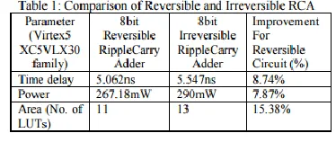
Furthermore, various parameters of reversible and non reversible adders were observed and compared and are tabulated in Table 1.
TABLE 2.1
3.2.Wallace tree multiplier:
The entryway utilized as a part of actualizing a reversible swell convey full viper is the TSG door [4]. The TSG entryway capacities like a full snake. A reversible swell convey snake is speedier than the non-reversible viper, since the calculation of convey in a reversible snake does not require the calculation of past stage convey (as showed in the basic ways). At the point when past stage convey is being sent in
the reversible viper, the calculation of past stage convey and calculation with respect to entirety is done at the same time though in an irreversible snake the following stage convey can't begin any calculation till past stage convey is completely created. The basic ways of 4bit reversible and irreversible swell convey adders is shown in fig. 8:
FIG:8 Wallace tree multiplier
Table 2: Comparison of Reversible and Irreversible Wallace Tree Multiplier
3.3Design of control unit for GCD processor:
To represent the established and reversible ways to deal with the Sequential Control Unit Design, reversible rationale is utilized for an uncommon reason processor that figures the GCD of two numbers. This GCD processor fuses standard Euclid's
Algorithm including Subtract-Compare-Swap
operation of two numbers. The essential standard is to subtract littler of the two numbers over and over from the other number until we get the number that partitions another [6]. A. Control Unit Control unit of GCD processor creates the control signs to control the operations in Data-way
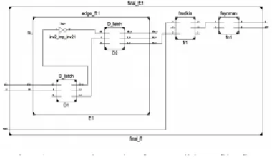
Fig. 9: Block diagram of GCD Control Unit B. Block Diagram Description:
1) Flip-flop Module: The control unit for GCD processor requires two Flipflops as binary state encoding is used for FSM. In this design reversible edge-triggered D Flip-flop is employed for state transitions [7]. Two D-latches are connected in Master-Slave mode to act as an edge-triggered D Flip-flop. Reversible D-latch is designed using Feynman and Fredkin gates [8]. RTL schematic of reversible D flip-flop obtained is shown in fig. 10:
Fig. 10: RTL schematic of Reversible D flip-flop
2)Regeneration Module To avoid multiple fan-out condition in the design, it is necessary to duplicate signals used for computation of output and next state. The duplication of input signals is achieved using Feynman gates.
3) Output Module The computation of the outputs and Next-state signals is done using reversible Fredkin gates. The functioning of output signals is driven by the algorithm. C. Final RTL schematic: The complete RTL schematic of GCD control unit is shown in fig. 11.
D. Speed and power analysis:
Table 3: Comparison of Reversible and
Irreversible Control 3.4 Decoder:
The Design of Combinational and
Sequential Circuits hasbeen ongoing in research. Various proposals are given for thedesign of
subtractors,multiplexers, decoders etc., in the existing method the authorhas given a novel design of 4x16 decoder whose Quantum Costis less than the previous design. Replacing fredkin gates fordesigning 2×4 decoder reversible gates like peres gate, TRgate, NOT gate and CNOT gate are used as shown in figure9.The whole design is done using Fredkin, CNOT, Peres gateswhich give better Quantum Cost when compared to the other
reversible Logic gates. The number of gates required to design4x16 decoder are 18 in which there are 12 fredkin gates, oneperes gate, one TR gate, one NOT gate and 3 CNOT gates. Thesum of all the quantum costs of each gate gives total quantumcost of 4x16 decoder.Different Reversible Decoder circuits like 2×4, 3×8, 4×16are designed using Fredkin Gates (mainly), Feynman gates andPeres gate. Some combinational circuits like comparator adder,subtractor, multiplexers etc., are designed using these decoders.The concept of duplicating a single output to required numberof outputs using Feynman gate is introduced where Fan-outwas not allowed in reversible computation.
IV. SIMULATION RESULTS
Output of reversible decoder:
Output of carry save adder:
Output of d-f/f:
Output of full adder/subtractor:
Output of sr flip-flop:
V.CONCLUSION
In this project, it can be seen that the performance of digital circuits can be enhanced using reversible gates and have compared 8-bit ripple carry reversible adder with an irreversible adder in terms of speed and power; thereby concluding that reversible designs are faster and power efficient. Furthermore, this concept is extended to combinational circuits such as a Wallace tree multiplier using reversible gates, which were simulated and respective results validate prior inferences. Then a reversible sequential control unit of a GCD processor was designed. Thus, all the designs implemented were compared with their irreversible counterparts, and the speed and power parameters for the reversible designs were observed to have improved significantly.
In this project, different combinational circuits like fulladder, full subtractor, multiplexer, comparator circuitsconstructed using reversible decoder are designed. Thesecircuits are designed for minimum quantum cost andminimum garbage outputs. The method proposed fordesigning the decoder circuit can be generalized. For example,a 3×8 decoder can be designed using a 2×4 decoder followedby 4 fredkin gates, Similarly a 4×16 decoder can be designedusing 3×8 decoder followed by 8 fredkin gates .The concept ofduplicating the single output to required number of outputs isutilized to overcome the fan-out limitation in reversible
logiccircuits. This method of designing
combinational circuit helps to implement many digital circuits with betterperformance for minimum quantum cost.
REFERENCES
[1] Landauer, Rolf, "Irreversibility and heat generation in the computing process," IBM Journal of Research and Development , vol.44, no.1.2, pp.261,269, Jan. 2000
doi: 10.1147/rd.441.0261
[2] Bennett, C.H., "Logical Reversibility of Computation," IBM Journal of Research and Development , vol.17, no.6, pp.525,532, Nov. 1973 doi: 10.1147/rd.176.0525
[3] B, Raghu Kanth; B, Murali Krishna; G, Phani Kumar; J, Poornima, “A Comparative Study of Reversible Logic Gates”, InternationalJournal of VLSI & Signal Processing Applications, vol.2, Issue 1, Feb 2012, (51-55), ISSN 2231-3133 ( Online ). [4] Morrison, M.; Ranganathan, N., "Design of a Reversible ALU Based on Novel Programmable Reversible Logic Gate Structures," VLSI (ISVLSI), 2011 IEEE Computer Society AnnualSymposium on , vol., no., pp.126,131, 4-6 July 2011
doi: 10.1109/ISVLSI.2011.30.
[5] Nachtigal, M.; Thapliyal, H.; Ranganathan, N., "Design of a reversible single precision floating point
multiplier based on operand decomposition,"
Nanotechnology (IEEE-NANO), 2010 10thIEEE
Conference on , vol., no., pp.233,237, 17-20 Aug. 2010
doi: 10.1109/NANO.2010.5697746 (Nachtigal,
Thapliyal, &Ranganathan, 2010)
[6] John P. Hayes, "Computer Architecture and Organization", McGraw-Hill, 1998. ISBN 10:
0070273553 / ISBN 13: 9780070273559
[7] Min-Lun Chuang; Chun-Yao Wang, "Synthesis of Reversible Sequential Elements," Design Automation Conference, 2007. ASPDAC'07. Asia and South Pacific , vol., no., pp.420,425, 23-26 Jan. 2007 doi: 10.1109/ASPDAC.2007.358022