Thesis by
Dong Yoon Oh
In Partial Fulfillment of the Requirements for the degree of
Doctor of Philosophy
CALIFORNIA INSTITUTE OF TECHNOLOGY Pasadena, California
2018
© 2018
Dong Yoon Oh
ORCID: 0000-0001-6716-1851
ACKNOWLEDGEMENTS
Thank you Jesus, my Lord and my Savior, for saving me and bringing me to your light during my senior year at Caltech. Once you met me, I could never be the same person. Thank you for letting me taste the abundant life in you and the joy of following you. I also thank you for carrying me through the years of graduate school, during which I barely scratched the surface of the field of optics and photonics, but I was tremendously blessed to see your wonder. All the praise and glory belong to you.
I thank my advisor Professor Kerry Vahala for his guidance and mentorship through-out my graduate study. In mid-March of 2012, I had the first meeting with Kerry in Watson 234 at Caltech. After praying through the week, I decided to stay at Caltech for another 5 years. Even though his schedule was often filled with meetings, trips and classes, Kerry has always made himself available whenever I wanted to discuss about research with him. It has also been also a privilege for me to work on some of the most exciting photonic devices operating in the nonlinear optics regime. Being involved in a team of research groups developing system-level applications like an optical synthesizer and a two-photon optical clock broadened my views on pho-tonics. One of the highlights at the end of graduate school was the opportunity of visiting the Mauna Kea summit and Keck Observatory with Kerry, his son Jonathan, Seung Hoon and Greg before my postdeadline talk at the 2017 Nonlinear Optics Meeting. Thank you for making my graduate school journey an unforgettable one.
I am very thankful for the opportunities I had to work with Dr. Scott Diddams. I benefited a lot from the breadth and depth of his knowledge in various experiments. I appreciated all his advice, comments and suggestions that he kindly provided. I thank him for having me visit his lab in early 2016 and the privilege to see our silica ridge waveguides in action as well.
My gratitude goes out to all my labmates in the Vahala group. Over the past years, I worked closely with Ki Youl Yang on several projects. I learned a lot from his in-depth knowledge of microfabrication and the discussions we had. I thank Seung Hoon Lee for building the first butt-coupling setup in our lab and all the other contributions he made in the integrated UHQ resonator project and the visible soliton project. I would also like to thank Boqiang Shen, who worked together with me in various measurements, modeling and layout designs towards the end of my graduate school years. Yu-Hung Lai has generously spent time to fabricate new taper fibers when I needed them. The advice from Xu Yi and Qi-Fan Yang were helpful for my soliton experiments. I thank Hansuek Lee for fabricating the spiral wedge waveguides and David Sell for his contribution as a SURF student in our first supercontinuum generation project. I thank Myoung-Gyun Suh, Xinbai Li and Heming Wang for being great colleagues.
I thank Pastor Ray and Jackie, who have walked alongside me and always encouraged to seek Jesus above all else. Daniel, Sora, Matthew and Emma have been role models for me as a young believer. The verse "Iron sharpens iron, and one man sharpens another" applies to my friendship with Andre. I praise God for giving me a brother to pray with in the ups and downs. Joel has always been an encouraging brother to me. I’m truly thankful to brother David, Seongho, Peter, Jimmy and John.
I cannot describe with words how blessed I am to be on this journey together with my wife Elaine. I am deeply grateful for her whose love and prayers supported me throughout the years. A few months ago, God gifted us a new life yet to be born. We thank God for his tremendous blessings in our lives.
ABSTRACT
PUBLISHED CONTENT AND CONTRIBUTIONS
[1] D. Y. Oh*, K. Y. Yang*, C. Fredrick*, G. Ycas, S. A. Diddams, and K. J. Vahala. “Coherent ultra-violet to near-infrared generation in silica ridge waveguides”. In:Nature Communications8 (2017).
D.Y.O participated in conception of the project, performed the modeling, designed mask layouts, did SEM characterization, assisted in the fabrication, built the 830 nm setup, measured the devices, co-demonstrated the shortest-wavelength-to-date on-chip UV dispersive wave generation, prepared the data and participated in the writing of the manuscript., p. 13922. doi:10. 1038/ncomms13922.
[2] S. H. Lee*, D. Y. Oh*, Q.-F. Yang*, B. Shen*, H. Wang*, K. Y. Yang, Y. H. Lai, X. Yi, X. Li, and K. Vahala. “Towards visible soliton microcomb generation”. In:Nature Communications8 (2017).
D.Y.O participated in the conception of the project, contributed in the mod-eling and fabrication of devices, built the 778 nm testing setup, measured the devices, demonstrated the soliton microcombs operating at the shortest-wavelength-to-date, prepared the data and participated in the writing of the manuscript. doi:10.1038/s41467-017-01473-9.
[3] D. T. Spencer et al. “An Integrated-Photonics Optical-Frequency Synthe-sizer”. In:arXiv preprint arXiv:1708.05228(2017).
D.Y.O co-invented and developed integrated ultra-high-Q resonators gener-ating electronically-compatible-rate soliton microcombs for optical synthe-sizer.
[4] K. Y. Yang*, D. Y. Oh*, S. H. Lee*, Q.-F. Yang, X. Yi, and K. Vahala. “Bridging ultra-high-Q devices and photonic circuits”. In: arXiv preprint arXiv:1702.05076(2017).
D.Y.O participated in the conception of the project, designed mask layouts, contributed to the modeling, measured the devices, co-demonstrated an inte-grated optical resonator with highest-Q-to-date, the soliton microcomb and stimulated Brillouin laser operation using the integrated devices, prepared the data and participated in the writing of the manuscript.
[5] D. Y. Oh, D. Sell, H. Lee, K. Y. Yang, S. A. Diddams, and K. J. Vahala. “Supercontinuum generation in an on-chip silica waveguide”. In: Optics letters39.4 (2014).
D.Y.O participated in the conception of the project, performed the modeling and the measurement, prepared the data, and participated in the writing of the manuscript., pp. 1046–1048. doi:10.1364/OL.39.001046.
PUBLISHED CONTENT - CONFERENCE PAPERS
[2] D. Y. Oh*, Q.-F. Yang*, S. H. Lee*, H. Wang*, B. Shen*, K. Y. Yang, Y.-H. Lai, X. Yi, and K. J. Vahala. “Towards Visible Soliton Microcomb Gener-ation”. In: Nonlinear Optics. Optical Society of America. 2017, NTh3A– 3.
[3] S. H. Lee*,D. Y. Oh*, K. Y. Yang*, Q.-F. Yang, X. Yi, and K. J. Vahala. “In-tegrable Soliton Microcomb at Microwave Repetition Rates”. In:Nonlinear Optics. Optical Society of America. 2017, NM1A–2.
[4] C. Frederick, D. Y. Oh, K. Y. Yang, G. Ycas, K. J. Vahala, and S. Did-dams. “Silica-Chip-Based Continuum Generation for Frequency Comb Self-Referencing”. In: Frontiers in Optics. Optical Society of America. 2016, FTh5G–3.
[5] D. Y. Oh*, K. Y. Yang*, and K. J. Vahala. “On-chip UV dispersive wave generation”. In:CLEO: Science and Innovations. Optical Society of Amer-ica. 2016, SF2O–4.
[6] K. Y. Yang*,D. Y. Oh*, S. H. Lee*, and K. J. Vahala. “Ultra-high-q silica-on-silicon ridge-ring-resonator with an integrated silicon nitride waveg-uide”. In:CLEO: QELS_Fundamental Science. Optical Society of America. 2016, JTh4B–7.
[7] D. Y. Oh, D. Sell, H. Lee, K. Y. Yang, S. A. Diddams, and K. J. Vahala. “Su-percontinuum generation in a silica spiral waveguide”. In: CLEO: Science and Innovations. Optical Society of America. 2014, STh1I–3.
TABLE OF CONTENTS
Acknowledgements . . . iii
Abstract . . . v
Table of Contents . . . viii
List of Illustrations . . . x
Chapter I: Introduction . . . 1
1.1 Thesis outline . . . 2
1.2 Nonlinear response of dielectric materials . . . 3
1.3 Pulse propagation in waveguides . . . 5
Chapter II: Integrated Ultra-High-Q Optical Resonators . . . 9
2.1 Abstract . . . 9
2.2 Introduction . . . 9
2.3 Silica ridge resonator design . . . 12
2.4 Design of a single mode silicon nitride waveguide phase-matched to a silica ridge resonator . . . 16
2.5 Fabrication process . . . 19
2.6 Experimental demonstration of waveguide-resonator coupling . . . . 21
Chapter III: Demonstration of Nonlinear Optics in Integrated Ultra-High-Q Resonators . . . 24
3.1 Abstract . . . 24
3.2 Introduction . . . 24
3.3 Soliton comb generation . . . 26
3.4 Stimulated Brillouin laser operation . . . 28
3.5 Summary . . . 29
Chapter IV: Towards Visible Microresonator-Based Soliton Frequency Combs 30 4.1 Abstract . . . 30
4.2 Introduction . . . 30
4.3 Dispersion engineering of silica microresonators . . . 35
4.4 Design of soliton devices at pump wavelength 1550 nm, 1064 nm and 778 nm . . . 37
4.5 Soliton frequency comb generation using 1um pump . . . 39
4.6 Soliton frequency comb generation using 778 nm pump . . . 43
4.7 Summary . . . 46
Chapter V: Supercontinuum Generation in Ultra-Low-Loss Silica Waveguides 50 5.1 Abstract . . . 50
5.2 Introduction . . . 50
5.3 Experimental demonstration of supercontinuum generation . . . 50
5.4 Modeling ultra-low-loss silica spiral waveguides . . . 52
6.1 Abstract . . . 56
6.2 Introduction . . . 56
6.3 Silica ridge waveguide array . . . 59
6.4 Dispersive wave generation . . . 63
6.5 Application: self-referencing of a frequency comb . . . 68
6.6 Spectral measurements . . . 71
6.7 Summary . . . 77
LIST OF ILLUSTRATIONS
Number Page
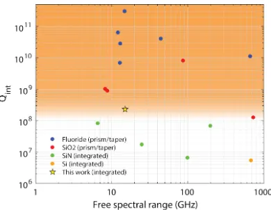
2.1 State-of-the-art ultra-high-Q optical microresonator platforms Review of the optical microresonators that have demonstrated high-est Q. The intrinsic quality factors (Qint) are plotted versus free
spectral range for various resonator material platforms and coupling schemes. The orange background represents the ultra-high-Q regime (> 108), which previously have been accessible only by prism- or taper-coupled resonators. . . 11 2.2 Integration of chemically etched silica resonator with a waveguide
(a) Schematics of silica wedge resonator. Taper fiber is used for coupling of light into the resonator. (b) Schematics of silica ridge resonator integrated with silicon nitride waveguide. Because of the base silica layer, a waveguide can be monolithically integrated with the resonator. . . 13 2.3 Calculated quality factor of a wedge resonator as a function of
the resonator thickness(a) Intrinsic quality factor (Qint) versus the
resonator thickness (t, indicated by the arrows inb) of a silica wedge resonator for the fundamental TE and TM mode families. (b) The fraction of electric field energy near the surface (defined in the text). Calculated mode profiles of the fundamental modes are shown as an inset. The arrows at the electric field intensity maximum represent the direction of the electric field. In general, the TM1 mode has
higher Q factor than the TE1mode due to the weaker electric field at
the silica-air boundary . . . 14 2.4 Optimization of base silica layer thickness (a) Intrinsic quality
factor (Qint) versus base layer thickness (t2, indicated by the arrows
inb) of a silica ridge resonator for the fundamental TE and TM mode families. (b) Calculated mode profiles of the fundamental modes at
2.5 Effective index of the TE11mode of the silicon nitride waveguide
(a) Calculated mode profile of the TE11mode of the SiN waveguide.
(b) Calculated effective index (neff) of the TE11 mode as a function
of the waveguide width W and thicknessT denoted ina. The white solid line indicates the pairs (W,T) for which the effective index of the SiN waveguide matches the effective index (1.438) of the TM1 mode of the silica ridge resonator. . . 19 2.6 Design of the single mode SiN waveguide(a) Effective indices of the
SiN waveguide modes are plotted as functions of the waveguide width
W. The waveguide thicknessT is 250 nm. (b) The calculated mode profiles of low-order modes (TE11, TE21, TE31) for the waveguide
with W = 4 µm are shown as inset . . . 20 2.7 Fabrication process for integrated ultra-high-Q microresonator
(a) Silica disk is defined on silicon by photolithography and HF etching of an initial silica layer. (b) Thermal oxidation grows a second oxide layer beneath the etched silica disk. (c) PECVD silicon nitride is deposited. (d) Silicon nitride waveguide is defined on silica layer by lithography and etching. (e) Lithography and wet etch of the silica define a ring aperture to the silicon substrate. (f) XeF2 etches
the silicon through the ring aperture. . . 21 2.8 Integrated ultra-high-Q microresonator (a) Rendering showing
2.9 Spectral scan of integrated ridge resonator and ring-down mea-surement(a) Spectral scan encompassing two free-spectral-ranges. (b) High resolution zoom-in scan for the TM1 and TE1 modes with intrinsic (Qo) and loaded (Q) quality factors, as well as the linewidth (κ/2π) indicated (M = million). The green sinusoidal signal is a
frequency calibration scan using a radio-frequency calibrated fiber Mach-Zehnder interferometer (free-spectral range is 5.979 MHz). (c) Superposition of 10 cavity-ringdown signal scans for the TM1 mode with the corresponding decay time and the loaded and intrinsic Q factors. . . 23 3.1 Demonstration of detectable repetition rate temporal solitons
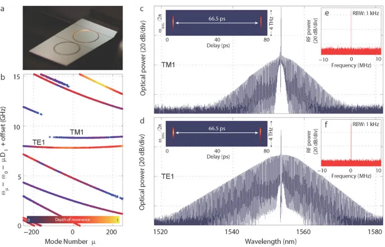
in an integrated optical microresonator (a) Photograph of a sil-icon chip with two integrated silica ridge resonators. (b) Measured mode frequencies plotted versus mode number for all the waveguide-coupled cavity modes with linear dispersion removed. (b) Optical spectrum of soliton with pump line indicated. Inset shows the elec-trical spectrum of the detected soliton pulse stream (RBW: resolution bandwidth) (c) FROG scan of single soliton state in 3b showing the single pulse signal with pulse period of 66.5 ps corresponding to resonator round-trip time. . . 27 3.2 Demonstration of Brillouin lasing in an integrated optical
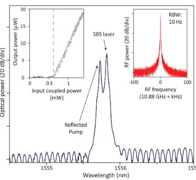
mi-croresonator Optical spectrum of Brillouin laser. The left inset demonstrates the output laser power vs. input coupled power. These data shows laser threshold behavior and the measured threshold power is as low as 250 µW. The right inset shows RF beat of the back-reflected pump and lasing signal. . . 28 4.1 Clock wavelengths of single ions and many neutral atoms used in
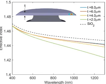
4.2 Effective index of fundamental TM mode (TM1) of silica wedge resonators for various thickness t Effective index of TM1 mode of the resonator versus wavelength is plotted for various thicknesst. The dashed line is the refractive index of fused silica based on the Sellmeier eqation. A schematics of silica wedge resonator is shown as an inset to the figure. . . 34 4.3 Calculated dispersion of the TM1 mode(a) Total dispersion(β2) is
plotted versus wavelength for various t. The dashed line indicates the material dispersion of silica (b) Geometrical dispersion(β2,geo),
de-fined as the total dispersion(β2) subtracted by the material dispersion
of silica dispersion(β2,SiO2) . . . 34
4.4 Calculated electric field intensity of TM1 mode of the resonator for various thicknesstand wavelengthsλ. Mode field intensity for t = 8,4,2 µm andλ= 400, 600, 800, 1000 nm is shown. The wedge angle is fixed at 30 degree for these simulations. At small t and/or large λ, the radial position of the mode intensity maximum moves out of the wedge, and its vertical position does not change any more. In this regime, the geometrical dispersion of the mode is anomalous (See the main text for further details). . . 36 4.5 Fabricated silica wedge resonator devices that feature anomalous
dispersion at pump wavelength 1550 nm, 1064 nm and 778 nm. (a) Regions of normal and anomalous dispersion are shown versus silica resonator thickness (t) and pump wavelength. The zero dispersion wavelength (λZDW) for the TM1 mode appears as a blue curve. Plot is
made for a 3.2-mm-diameter silica resonator. Three different device types I, II and III (corresponding to three oxide thicknesses) are indicated for soliton generation at 1550 nm, 1064 nm and 778 nm. (b) Cross-sectional SEM images of the fabricated resonators. White scale bar is 5 µm. . . 38 4.6 Measured Q factors and comb threshold powers versus thickness
and pump wavelength for the three device types. Effective mode area (Aeff) of the TM1 mode family is also plotted as a function of
4.7 Soliton frequency combs at pump wavelength 1550 nm, 1064 nm and 778 nmSoliton frequency comb spectra measured using device types I, II and III designed for pump wavelengths 1550 nm, 1064 nm, and 778 nm, respectively. Pump frequency location is indicated by a dashed vertical line. The soliton pulse repetition rate of all devices is about 20 GHz. Insets: cross-sectional SEM images of the fabricated resonators. White scale bar is 5 µm. . . 40 4.8 Microresonator dispersion engineering at 1064 nm. (a) Simulated
dispersion (GVD) of TM mode families versus resonator thickness. The angle of the wedge ranges from 30◦to 40◦in the colored regions. Measured data points are indicated and agree well with the simulation. (b) Measured relative mode frequencies (blue points) plotted versus relative mode number of a soliton-forming TM1 mode family in a 3.4 µm thick resonator. The red curve is a parabolic fit yielding
D2/2π=3.3 kHz. . . 41
4.9 Experimental setup for soliton generation. A continuous-wave (CW) fiber laser is modulated by an electro-optic phase modulator (PM) before coupling to a ytterbium-doped-fiber-amplifier (YDFA). The pump light is then coupled to the resonator using a tapered fiber. Part of the comb power is used to servo-lock the pump laser frequency. FBG: fiber Bragg grating. PD: photodetector. PC: polarization controller. . . 42 4.10 Soliton generation at 1064 nm. Optical spectra of solitons at 1064
4.11 Mode hybridization at 778 nm illustrated by the effective indices of the resonator modes (a) Calculated effective indices for TE1, TE2, TM1 and TM2 modes at 778 nm plotted versus thickness for a silica resonator with reflection symmetry. The TM1 and TE2 modes cross each other without hybridization. The dashed box is the frame for the panel bzoom-in. (b) Zoom-in of the dashed box in panel a. Inset shows resonator with reflection symmetry (equivalent to wedge angleθ= 90◦). (c) As inbbut for resonator withθ= 40◦. An avoided crossing of TM1 and TE2 occurs due to mode hybridization. . . 43 4.12 Calculated GVD of the two hybrid modes for θ = 40◦.
Hy-bridization causes a transition in the dispersion around the thickness
ttr = 1.48µm. The points are the measured dispersion values. . . 44 4.13 Measured mode frequencies of the hybrid modes (a) Measured
relative mode frequencies of the TM1 and TE2 mode families versus relative mode number µfor devices witht = 1.47. The thickness is below the transition thickness ttr and the TM1 mode is anomalous.
(b) As inabut fort = 1.49µm. The thickness is above the transition thicknessttrand the TE2 mode is anomalous. . . 44
4.15 First soliton microcomb demonstration at 778 nm (a) Measured mode frequencies of the TM1 mode family plotted versus wavelength for a t = 1.47 µm device. The pump wavelength is indicated as a dashed line. The spurs in the data are due to the crossing with other mode families. (b) Optical spectrum of a soliton with pump line (778.7 nm) indicated. The red curve is a simulation using the Lugiato-Lefever equation including the Raman terms, which deviates slightly from the sech2 envelope due to the higher order dispersion. The spectral location of observed dispersive waves match well with the mode crossing locations ina, revealing that the dispersive waves are induced by spatial mode-interactions[yang2016spatial.] Inset shows the electrical spectrum of the detected soliton pulse stream. . . 48 4.16 Generation of a soliton microcomb that spans wavelengths 755
-793 nm. (a) Measured mode frequencies of the TM1 mode family plotted versus wavelength for a t = 1.50 µm device. (b) Optical spectrum of a soliton with pump line (778.7 nm) indicated. The red curve is a simulation using Lugiato-Lefever equation including the Raman terms. Inset shows the electrical spectrum of the detected soliton pulse stream. . . 49 5.1 Low-loss, silica-on-silicon waveguide and experimental setup. (a)
Photograph of the sample showing four, cascaded spiral waveguides. (b) Experimental setup for supercontinuum generation and charac-terization using the silica waveguide. OPO: optical parametric os-cillator; OSA: optical spectrum analyzer. (c) Close-up view of the optical coupling stage, imaging objectives and spiral waveguide chip. 51 5.2 Spectral broadening in the fundamental TM mode measured at
a series of pulse energies. The blue curves are measured spectra, and the dashed curves in light blue are spectra from the simulation. . 53 5.3 Calculated dispersion and nonlinearity of the fundamental TM
mode at a series of bending radii that occur at the inner and outer
waveguides within each spiral. . . . 54 6.1 Overview of on-chip waveguide platforms for supercontinuum
6.2 Silica ridge waveguide structure. Scanning electron microscope images of an array of silica ridge waveguides on a silicon chip. Silicon pillars support silica layers containing waveguides. The red box in panel (a) contains a silica waveguide whose cross section is shown as the inset. The cross section shows the calculated mode profile of the TM mode at wavelength 830 nm superimposed. Scale bar is 100µm for (a) and 1µm for the inset. . . 58 6.3 Ridge waveguide array microfabrication process. (a)
Photolithog-raphy on thermal silica layer. Mask width is denoted by the double-arrow line. (b) HF wet-etching to define silica ridge. (c) Additional oxide layer is grown by thermal oxidation. (d) Supporting structure is patterned by photolithography. (e) HF wet-etching creates striped openings in the silica layer. (f) Isotropic etching of the silicon (XeF2)
is performed to undercut the silica layer. (g) Rendering of final ridge waveguide array structure. Dependence of ridge dimension on mask width is shown in Figure 6.4. . . 60 6.4 Dependence of ridge dimension on mask width (a) SEM images of
a series of ridges in a fabricated silica waveguide array. The thickness of the base silica layer is 0.45 µm. Scale bar is 1 µm. The definition of ridge height(H) and ridge width(w) is shown in the panel. (b) Measured ridge dimensions based on SEM images as a function of mask width . . . 61 6.5 Dispersion engineering of ridge waveguides. (a) Calculated mode
area and zero dispersion wavelength (λZDW) are plotted versus the
ridge base width. (b) Calculated mode area and zero dispersion wave-length (λZDW) are plotted versus the ridge base width. Calculated
6.6 Phase-matching dispersive wave wavelength in a waveguide array. Calculated TM dispersive wave wavelength (λDW) as a function of
pump wavelength and ridge width is plotted as a colormap for the waveguide array chip used in Figure 6.8e. The black lines are the zero crossing of the group velocity dispersion(λZDW,1 and λZDW,2).
The white area is where dispersive waves do not exist. . . 64 6.7 Experimental setup for supercontinuum generation using a
tita-nium sapphire laser centered at 830 nm. The pulses entering the ridge waveguides have FWHM temporal width of 60 fs. . . 65 6.8 Direct observation of dispersive wave generation UV-visible
6.9 Numerical simulation of pulse propagation in the waveguide and comparision with measurement. (a) Calculated continuum spectra as a function of waveguide position at a coupled pulse energy of 330 pJ. The pulse is launched in the TM mode of the waveguide with mode area 0.76 µm2. The color bar (inset) applies to panels (a), (c), (d) and (e). (b) Top-view photographs of scattered light from the surface of the waveguide. The photographs were taken at pulse energies ranging from 330 pJ to 1100 pJ (left to right side). As indicated by the dashed line, the pulse travels in the waveguide from the bottom to the top of the image. Dispersive wave generation occurs in the UV and is therefore not visible in the image. The grey line superimposed on the photographs is the length at which dispersive wave generation occurs as predicted by the simulation. The spectral breathing of the input pulse results in a periodically visible orange-red emission that correlates with the calculation. (c) Calculated continuum spectra as a function of waveguide position at a pulse energy of 1100 pJ. (d-e) Calculated spectrograms of the optical pulse propagating in the waveguide corresponding to (c). The spectrogram in (d) is at waveguide position 0.16 cm where dispersive wave is generated. The spectrogram in (e) is at the waveguide output. . . 67 6.10 Application of dispersive wave engineering to self-referencing a
Yb fiber laser frequency comb. (a) Experimental setup for measur-ing fceo of the Yb fiber laser. The ridge waveguide has a mode area
3.13 µm2 and length 1.50 cm. (b) Photograph of the emitted light dispersed through a prism and reflected on a white screen. Scale bar is 5 cm. (c) Measured optical spectrum of the collimated beam at the output facet of the waveguide. The coupled pulse energy is 2300 pJ and the input spectrum is shown in black. (d) Spectra of the disper-sive wave (DW, blue) and second harmonic light (SH, black) filtered by a bandpass filter. (e) Radio-frequency spectrum measured with an electrical spectrum analyzer (ESA) shows the pulse repetition rate
frep and the carrier-envelope-offset beat frequency fceo,1 and fceo,2.
6.11 Calculated temporal delay of the pulse used for f-2f measurement. (a) Relative group delay between TE and TM mode at the end of the waveguide of length 1.5 cm. Delay is set to 0 for TE mode at the pump wavelength of 1064 nm. The dashed line is located at the pump wavelength of 1064 nm. (b) Spectrogram of the TE portion of the pulse at the end of the waveguide. As in panel (a), y-axis represents the relative group delay with respect to the group delay at the pump wavelength 1064 nm . . . 70 6.12 Supercontinuum spectra generated in the TE and TM mode of the
waveguides. Supercontinuum spectra for a series of ridge waveguides on a single waveguide array chip shown in Figure 6.8 when the titanium sapphire laser pulse is coupled to the TM mode (blue line) and TE mode (red line) of the waveguides. The coupled pulse energy is 1000 pJ. The mode area of the waveguide is indicated in the panel. All the continuum spectra are normalized such that the areas under the spectra are the same. . . 72 6.13 Precisely tuned and efficient emission of dispersive waves in the
UV-visible wavelengths. (a) Measured tuning of the dispersive wave peak wavelength (λDW) by lithographic control of the waveguide
mode effective area. The data are taken for a pulse energy at the dispersive wave generation threshold. The solid line is the phase matching condition obtained from FEM simulations. (b) Scatter plot of measured conversion efficiency (left axis) and dispersive-wave average power (right axis) versus the dispersive dispersive-wave peak wavelength for the waveguide array in Figure 6.8. Blue and red markers correspond to the TM mode and the TE mode. The coupled pulse energy is 1000 pJ. . . 73 6.14 Measured UV dispersive wave spectra and the conversion
6.15 Waveguide deformation and its remedy by annealing (a-c) SEM images showing the deformation at the position where soliton fission point occurs. The waveguide of mode area 0.86 µm2was used and the dispersive wave peak was located at 345 nm. (d) Continuous measurement of UV power generated from an annealed waveguide of similar dimension as ina-c. A fresh waveguide without deformation was annealed at 1000 degree for 24 hr. The average coupled power was 41 mW. . . 75 6.16 265 nm generation. Measured dispersive wave spectra in deep UV
when the Yb laser pulse is launched into the TM mode of 0.75 cm-long ridge waveguides having mode areas of 1.09 µm2(green) and 1.12µm2(black). The coupled pulse energy is 2000 pJ. . . 76 6.17 Spiral silica ridge waveguides. (a) Photographs of silica ridge
C h a p t e r 1
INTRODUCTION
From the birth of computers in the late 1930s, the evolution of the electronics and the communication systems has dramatically affected people’s lives in the past century. The time period is marked by the invention of transistors in 1947, the integrated circuit in 1958, the beginning of the world wide web in 1990 and is now facing the dawn of 5th generation wireless systems (5G). The impact of the photonics on the society has also significantly grown since the invention of laser in the 1960. In areas like biomedical imaging, medical surgery or manufacture, lasers have often found unprecedented applications due to the high coherence, directionality and power of the light they produce and the fact that their wave properties can be precisely controlled. The photonics also played a crucial role in the aforementioned historical advances. For instance, the birth of the fiber-optic communication in 1966 eventually led to the global deployment of fiber optic cables serving as the backbone of the high speed internet in the world wide web era.
An optical frequency comb (OFC), which emerged in 1999 - 2000 as a result of the union of ultrafast and ultra-stable laser technology, is a set of optical frequencies with equidistant spacing sharing the common phase and thereby producing temporal pulses in the time domain. It can be viewed as the collection of thousands of laser lines with constant spectral separation having coherent oscillations. Those laser lines are provided by a single laser consisting of a broadband gain medium, an optical cavity and a saturable absorber providing a mode-locking mechanism. OFCs have revolutionized the precision metrology and proven to enable the most precise time-keeping system on earth, the optical atomic clock. The fractional uncertainties of the best optical atomic clocks now reach the level of 1 over 1017[1]. Such precise clocks can be used in geodesy and high resolution global positioning system (GPS). OFCs also bring critical advances in many of the areas where optics and photonics have traditionally played vital roles including spectroscopy, astronomy, bioimaging and high-speed telecommunications. Furthermore, it works as a gear box between the microwave and the optical frequencies, providing the ability to control and synthesize the optical frequencies using the electronics[2].
science and optical technologies, the past decade has seen the rise of keen interests in miniaturizing such systems to chip-scale. Integrated photonic and optoelectronic chips have potentials for low-cost, scalable production as well as ready controls by users and will bring the diverse functionalities of OFCs out of labs. A pow-erful smartphone-size device that has various precision sensing capabilities and time-keeping function in the absence of GPS reception can be envisioned. Minia-turized combs can also be set up in environments that have stringent power and size requirements like telescopes for astronomical calibration[3] or spacecrafts for space-borne measurements[4]. They might also be integrated with the electronics in the data centers for petabit-per-second high-speed data transmission[5], meeting the rising demand from the ever-increasing volumes of data stored and transferred in cloud-based systems.
In this thesis, novel silicon chip-based devices that can serve as parts of the proposed integrated photonic systems are designed and tested.
1.1 Thesis outline
Chapter IIintroduces an integrated ultra-high-Q resonator achieving the record-high Q factor of 230 million. The silica ridge ring resonator is monolithically integrated with PECVD silicon nitride waveguide using standard microfabrication processes. The design, fabrication and characterization of the device are discussed.
Chapter III shows the multi-functionalities of the integrated UHQ resonator by demonstrating the electronics-compatible-rate (15 GHz) soliton microcomb and low-threshold Brillouin laser operation using the device. Both are the first demonstrations among the integrated microresonator platforms.
Chapter IV focuses on the progress made towards the visible soliton microcomb generation. A simple method of engineering the dispersion of the cavity is used to broaden the window of available pump wavelengths for bright soliton generation. 20 GHz soliton microcombs are generated using the pump at 1 µm and 778 nm. The shortest wavelength soliton-to-date is demonstrated covering the 755 - 790 nm band.
Chapter Vshifts the gear to the supercontinuum generation in on-chip silica waveg-uides. Supercontinuum generation in a 3.5-m long spiral waveguide is demonstrated and modelled using GNLSE.
waveg-uides are fabricated in a compact silicon chip, providing hundreds of choices of wavelengths. An application of the device in self-referencing of 1µm laser comb is demonstrated.
1.2 Nonlinear response of dielectric materials
Nonlinear polarization
When an electric field is applied to a medium, the medium is polarized in the following manner
P(t)=0χeffE(t) (1.1)
whereE(t)is the electric field,P(t)is the polarization,0is the vacuum permittivity
and χeffis the effective susceptibility. In the case where the applied electric field is
small enough, the polarization is proportional to the electric field and the effective susceptibility simply equals the linear susceptibility (χeff= χ(1)). This is true in the
regime of linear optics where the light intensity is small and the media that the light encounters or propagates through respond linearly. In a linear optical system, the frequencies of emitted light remain unchanged as they travel in media. For example, the optical frequency of monochromatic light passing through optical component like an optical lens or beam splitter stays constant.
In general, however, the response of dielectric media to the applied electric field has both the linear and nonlinear part. The nonlinear contribution becomes more pronounced when the electric field is stronger. In the absence of permanent dipole moments, the polarization can be described in the following power series expansion:
P(t)=0[χ(1)E(t)+ χ(2)E2(t)+ χ(3)E3(t)+...]
=P(1)(t)+P(2)(t)+P(3)(t)+... (1.2)
where χ(n) is the n-th order susceptibility represented as a n-th order tensor and P(n)(t) ≡ 0χ(n)En(t) is the n-th order nonlinear polarization. Equation 1.2 can be rewritten in terms of components of the electric field, polarization vectors and the nonlinear susceptibility tensors as follows:
Pi = 0[χ
(1) i Ei+ χ
(2)
i j EiEj + χ (3)
For a centrosymmetric medium (a material system that has the inversion symmetry), all the even order nonlinear susceptibilities vanish. This can be easily seen by substituting E,Pby −E,−P in Equation 1.2, requiring that the polarization in the opposite direction will result if an electric field of opposite direction is applied. For example, in the case of second-order polarization, the following holds true for a centrosymmetric medium:
Pi(2) = χi j(2)EiEj
−Pi(2) = χi j(2)(−Ei)(−Ej)
(1.4)
As a result, χ(2) = 0 and the material system cannot exhibit nonlinear optical processes originating from the second order susceptibility, which include second harmonic generation, sum-frequency generation, difference-frequency generation and optical parametric amplification.
Therefore, the third order nonlinearity is the lowest order nonlinearity possessed by a centrosymmetric medium and it is the cause of the most of the observed nonlinear optical processes.
Nonlinear optical processes arising from the third order nonlinearity
To examine the nonlinear optical processes that result from the third order nonlinear susceptibility universally present in most materials, let us examine the third order polarization : P(3)(t) = 0χ(3)
E3(t). The equation is written in a scalar form for simplicity of the following discussion. Let us assume that the electric field consists of three frequency componentsω1, ω2, ω3and can be written as
E(t)=
3
Õ
n=1
[E(ωn)e−iωnt+E(ωn)∗eiωnt] (1.5)
The polarizationP(3)(t)then has following terms:
χ(3)|
E(ωp)|2E(ωp)e−iωpt Self-phase modulation
χ(3)|
E(ωp)|2E(ωq)e−iωqt Cross-phase modulation
χ(3)
E(ωp)3e−i(3ωp)t Third harmonic generation χ(3)
E(ωp)E(ωq)E(ωr)e−i(ωp+ωq+ωr)t Non-degenerate Four-wave mixing
χ(3)
E(ωp)E(ωq)E(ωr)∗e−i(ωp+ωq−ωr)t Non-degenerate four-wave mixing
χ(3)
E(ωp)2E(ωq)e−i(2ωp+ωq)t Degenerate four-wave mixing χ(3)
where p, q, r can be any integer from 1 to 3 and p, q, r have different values from one another. The corresponding nonlinear optical processes include self-phase modulation, cross-self-phase modulation, third harmonic generation and four-wave mixing, which are indicated above.
In cases where the frequencies of the applied electric field are far off from the resonance frequencies of atoms or molecules, the components of the third order nonlinear susceptibility tensor in each term above can be calculated in a quantum mechanical model using the Schrodinger equation. There, we consider the interac-Ü
tion Hamiltonian ˆV(t) = −µˆ ·E(t) where ˆµ = −erˆ is the electric dipole moment. Treating this interaction Hamiltonian as a perturbation, one can derive a recursive series of equations for eigenfunctions. Then, the third order susceptibility can be calculated using the expectation value of the dipole moment per atom correct to the third order in perturbation theory. The formalism describes well the nonlinearities arising from the nonresonant electronic response of bound electrons, which are present in all the dielectric materials.
For a detailed discussion of the tensor nature of the nonlinear susceptibilities and their calculation using the perturbation theory, please see the work by Boyd[6].
1.3 Pulse propagation in waveguides
The derivation of Generalized Nonlinear Schrodinger Equation is taken from Agrawal,Ü
2007.
An optical waveguide is a device in which the optical field is confined and propagates along a certain direction. The propagation of optical fields in waveguides is governed by Maxwell’s equation:
∇ ×E=−∂B
∂t,
∇ ×H=J+ ∂D
∂t, ∇ ·D= ρf
∇ ·B=0
(1.6)
where E(H) is the electric(magnetic) field, D(B) is the electric(magnetic) field density,Jis the current density andρfis the charge density. In optical waveguides
Taking curl of the first equation and substitutingDby0E+PL+PNLwherePLand
PNLare the linear and nonlinear part of the polarization, respectively,
∇ × ∇ ×E+ 1
c2
∂2E
∂t2 + µ0
∂2P L
∂t2 +µ0
∂2P NL
∂t2 =0 (1.7)
where we used the relation c2 = 1
0µ0. Now, consider a pulse that propagates in a
waveguide mode that is polarized along ˆx-axis. Assuming that the pulse width is at least tens of optical cycles, we can use the slowly varying envelope approximation and write the electric field as E(r,t) = 12x[Eˆ (r,t)e−iω0t+ c.c], where E(r,t) is the
slowly varying envelope andω0is the center frequency of the pulse.
Now, we Fourier-transform this equation into the frequency domain to obtain the Helmholtz equation:
(∇2+(ω)ω
2
c2)E˜(r, ω)=0 (1.8)
We use the following separation of variables to solve for Equation 1.8.
˜
E(r, ω−ω0)= F(x,y)A˜(z, ω−ω0)eiβ0z (1.9)
whereβ0 ≡ β(ω0). Plugging Equation 1.9 into Equation 1.8,
∂2F
∂x2 +
∂2F
∂y2 +2iFβ0
∂A˜ ∂ze
iβ0z+((ω)ω
2
c2 −β 2 0)FAe˜
iβ0z (1.10)
Dividing Equation 1.10 byFAe˜ iβ0z,
1
F(
∂2F
∂x2 +
∂2F
∂y2)+
2iβ0
˜
A
∂A˜
∂z +(ω)
ω2
c2 − β 2
0 =0 (1.11)
We define ˜β(ω)such that
˜
β(ω)2 = 1 F(
∂2F
∂x2 +
∂2F
∂y2)+(ω)
ω2
c2 (1.12)
Then, it follows from Equation 1.11 that
−β˜(ω)2= 2iβ0
˜
A
∂A˜ ∂z −β
2
Equation 1.12 and 1.13 can be rewritten as
∂2F
∂x2 +
∂2F
∂y2 +((ω)
ω2
c2 −
˜
β(ω)2)F =0
2iβ0
˜
A
∂A˜
∂z +(β˜(ω)
2− β2 0)A˜ =0
(1.14)
The dielectric constant(ω)can be written as(ω)=(n+∆n)2where n is the linear refractive index given byn= p(1+ χ(1)). ∆nincludes contribution from the loss as well as the nonlinearity of the material. We consider the case in which the waveguide is made of χ(3)-material and make the following approximation: ∆n∼ n¯2|E|2+iα
(ω)
2k0
where k0 = 2λπ0 = 2ωπ0c and α(ω) is the loss of the waveguide at frequency ω. We treat∆n as a small perturbation and use the first-order perturbation theory to find the correction to the eigenvalue : β(ω) = β(ω)+∆(β(ω))where the correction is given by
∆β(ω)= ω
2n(ω)
c2β(ω)
∬∞
∞ ∆n(ω)|F(x,y)|
2dxdy
∬∞
∞ |F(x,y)|2dxdy
= ω
c
∬∞
∞ ∆n(ω)|F(x,y)|
2dxdy
∬∞
∞ |F(x,y)|2dxdy
=iα˜(ω)
2 + ωn¯2
c |A˜(z, ω−ω0)|
2
∬∞
∞ |F(x,y)|
4dxdy
∬∞
∞ |F(x,y)|2dxdy
(1.15)
The second and third line of Equation 1.15 are obtained by using β(ω)= n(ω)ωc.
With the approximation β(˜ω)2− β2
0= (β˜(ω)+β0)(β˜(ω) −β0) ∼2β0(β˜(ω) −β0), it
follows that
∂A˜
∂z =i(β˜(ω) − β0)A˜ =i(β(ω)+∆β(ω) − β0)A˜ (1.16)
Now, Equation 1.15 and lead to
∂A˜ ∂z =−
˜ α
2A˜+i(β(ω) − β0)A˜+iγ|A˜|
2 ˜
A (1.17)
γ(ω)= ωn¯2 c
∬∞
∞ |F(x,y)|
4dxdy
∬∞
∞ |F(x,y)|
2dxdy (1.18)
So far in our derivation, we have assumed that the nonlinear response of materials to incident optical field is instantaneous. However, in reality, ultrashort pulses cause delayed nonlinear responses from the material due to the Raman effect. The physical origin of the Raman effect is the molecular vibration of materials. Including the Raman response of silica,
∂A˜ ∂z =−
˜ α
2A˜+i(β(ω) − β0)A˜+iγF A˜
∫ ∞
0
R(t0)|A(z,t−t0)|2dt0
(1.19)
whereF denotes the Fourier transform and R(t)is the nonlinear response function given by
R(t)=(1− fR)(δ(t))+ fRhR(τ1−2+τ2−2)τ1e−t/τ2sin(t/τ1) (1.20)
Here, the first term represents the instantaneous electronic response where as the sec-ond term is related to the delayed Raman response. fRis the fractional contribution of delayed Raman response to the nonlinear polarizationPN L.
In the case of silica, the following formula agrees well with the experimental obser-vation:
hR =(τ1−2+τ2−2)τ1e−t/τ2sin(t/τ1) (1.21)
where fR= 0.18,τ1= 12.2 fs and τ2= 32 fs.
Equation 1.19 is the Generalized Nonlinear Schrodinger Equation(GNLSE) in theÜ
C h a p t e r 2
INTEGRATED ULTRA-HIGH-Q OPTICAL RESONATORS
[1] K. Y. Yang*, D. Y. Oh*, S. H. Lee*, Q.-F. Yang, X. Yi, and K. Vahala. “Bridging ultra-high-Q devices and photonic circuits”. In: arXiv preprint arXiv:1702.05076(2017).
2.1 Abstract
Optical microcavities[7] are essential in numerous technologies[8–12] and scientific disciplines[13, 14]. Applications, including inertial sensors[15–17], microcomb-related systems[8], microwave generation[18–21] and reference cavities/sources[22– 25], present challenging combinations of cavity Q-factor performance, phase-matching control and functional requirements. As a result, several critical applica-tions have to date only been demonstrated using discrete ultra-high-Q microcavities. Indeed, finding a scalable microfabrication pathway that preserves ultra-high-Q per-formance and other device perper-formance metrics while providing access to photonic integration has been a long-term priority of the microcavity field[7]. Here, an inte-grable ultra-high-Q microcavity is presented. Q factors as high as 230 million are achieved.
2.2 Introduction
Optical microcavities provide diverse functions that include frequency microcombs[8, 26], soliton mode-locked microcombs[27, 28], high-coherence Brillouin lasers[29], bio and nano-particle sensors[10–12], cavity optomechanical systems[14], para-metric oscillators[30, 31], Raman lasers[32], and strong-coupling cavity QED systems[33]. A figure of merit used to describe the performance of an optical microcavity is quality factor (Q) of its mode defined as
Q ≡2π Total energy stored in the cavity
Energy dissipated per cycle of light (2.1)
Here we assume that the optical energy is stored only in a specific mode of the cavity. Using the definition of Q, the temporal decay of energy in the cavity can be written as follows:
dU dt =−
U
where U is the total energy stored in the cavity,τ≡ Q/ω0andω0is the resonance
frequency of the mode. From Equation 2.2, we find that the stored energy decays as∼ e−t/τ and the electric field decays as∼ e−t/2τ. As such, we derive the electric field in the frequency domain as
E(ω)= √1
2π
∫ ∞
0
E0e−t/2τ+i(ω−ω0)tdt (2.3)
From this equation, the Lorentzian shape of a resonance is derived.
|E(ω)|2= E
2 0
2π[(1
2τ)2+(ω−ω0)2]
(2.4)
By defining the linewidth of the cavity ∆ω as the full width half maximum of the Lorentzian function, we get∆ω = 1/τ and Q = ω0/∆ω. Accordingly, the Q
factor of an optical microcavity can be characterized via a temporal scan (ring-down measurement to determine τ) or a spectral scan (linewidth measurement to determine∆ω).
Q−total1 =Q−rad1 +Q−abs1 +Q−surf1 +Q−cont1 +Q−ext1 (2.5)
Key performance metrics scale at least as 1/Q and frequently as 1/Q2 across all applications areas[7] and have accounted for a sustained period of progress in boosting Q factor by reducing optical loss in micrometer- and millimeter-scale resonators.
Microcavities that have achieved the highest Q factors share a common feature: they are whispering gallery mode (WGM) resonators in which the light is guided through total internal reflection occurring at the boundary of dielectric materials. The round trip optical path length and the group index of a whispering gallery mode determines the free spectral range (FSR), which is the frequency separation between adjacent modes and equals the repetition rate of the pulse in the case of mode-locking.
Figure 2.1 shows Qintplotted versus free spectral range for various material platforms
that have demonstrated the highest Q factors so far. The highest Q factor (Qint = 3
× 1011) was recorded with a 4.5 mm-diameter CaF2 resonator at wavelength 1550
Figure 2.1: State-of-the-art ultra-high-Q optical microresonator platforms Re-view of the optical microresonators that have demonstrated highest Q. The intrinsic quality factors (Qint) are plotted versus free spectral range for various resonator
material platforms and coupling schemes. The orange background represents the ultra-high-Q regime (>108), which previously have been accessible only by prism-or taper-coupled resonatprism-ors.
silicon cavity had a round trip length of 210 mm which corresponds to the FSR of 207 MHz. Silica microsphere (Q = 8×10⁹[37]), silica microrod (Q = 109[38]) and silica microtoroid (Q = 1.25×10⁸[39]) are made using heating techniquess (hydrogen flame or CO2 laser) to create a surface-tension-induced smooth and
round surface. Silica wedge resonator, fabricated using standard microfabrication process without an additional step of reflow by CO2laser, has proven to be a very
useful platform because of its high Q (reaching Q = 8.75×10⁸) and the precise controllability over its FSR usually ranging from∼5 to∼100 GHz[29].
the relative position of a resonator to the input optical path and has to be controlled through micropositioners and monitored through optical microscopes. This adds a significant complexity to the setup and limits potentials of ultra-high-Q microcavi-ties to be integrated with other on-chip photonic components and reliably deployed in their application areas that require small foot-print devices.
On the other hand, there has been keen interests in developing high Q resonators in integrated platforms. Such a new type of resonator can help realize the promises of optical microresonators to expand the functionalities of photonic integrated circuits (PICs). They can serve as narrowband filters, frequency references or modulators, and become essential building blocks for numerous PIC applications. Ultimately, systems-on-a-chip that have both the electronics and photonic components integrated together will bring significant impact to the landscape of industry. In recent years, a variety of resonator materials have been investigated. One of the most widely used materials is silicon nitride (SiN), which has a wide transparency window and low optical loss from visible to infrared wavelengths. The previous highest Q factor among integrated resonators was achieved in Si3N4[40–43]. Silicon has also been
investigated by research groups and showed promising results (Qint = 5×10⁶[44])
However, despite the remarkable progress in boosting the Q factors, there has been no report of integrated resonators whose Q factor exceed 100 million.
In this work, a monolithic microcavity featuring both a Q factor greater than 200 mil-lion and an integrated waveguide is demonstrated. The resonator is based on a novel silica ridge fabrication process and the waveguide is composed of plasma-enhanced chemical-vapor-deposited (PECVD) silicon nitride. The structure is fabricated on a silicon wafer using only standard lithography, wet etch, and dry etch steps. The materials, process steps and, in particular, the PECVD silicon nitride waveguide are compatible with other photonic devices. As a result, this process enables full integration of ultra-high-Q devices with other photonic devices on a silicon wafer.
2.3 Silica ridge resonator design
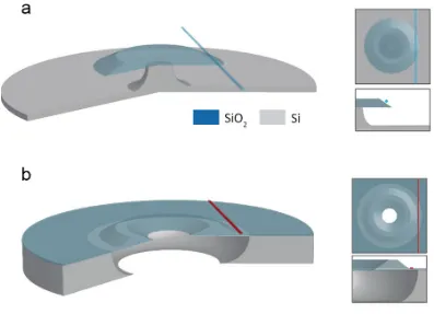
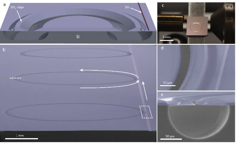
Figure 2.2: Integration of chemically etched silica resonator with a waveguide (a) Schematics of silica wedge resonator. Taper fiber is used for coupling of light into the resonator. (b) Schematics of silica ridge resonator integrated with silicon nitride waveguide. Because of the base silica layer, a waveguide can be monolithically integrated with the resonator.
create the smooth silica surface, wet-chemical etch is applied for a long duration to remove the rough line-shape features on silica created during initial wet-etch. As a result, the top of the silica layer retreats by about 12 µm from the edge of the photoresist pattern. The gap between adjacent patterns in silica layer is inevitably enlarged during the wet-etch following the lithography, which makes the integration of the silica wedge resonator with a silica waveguide nearly impossible. Therefore, the coupling to the silica wedge resonators has only been done using tapered fibers (See Figure 2.2a).
Figure 2.3: Calculated quality factor of a wedge resonator as a function of the resonator thickness(a) Intrinsic quality factor (Qint) versus the resonator thickness
(t, indicated by the arrows inb) of a silica wedge resonator for the fundamental TE and TM mode families. (b) The fraction of electric field energy near the surface (defined in the text). Calculated mode profiles of the fundamental modes are shown as an inset. The arrows at the electric field intensity maximum represent the direction of the electric field. In general, the TM1 mode has higher Q factor than the TE1
mode due to the weaker electric field at the silica-air boundary
ring resonator that is supported by silicon pillar from the outer side can be made as shown in Figure 2.2b. At the same time, a waveguide of a different material can be deposited, patterned and etched to provide a waveguide channel for coupling light into and out from the resonator. We choose PECVD silicon nitride (SiN) as the waveguide material because it has low optical loss and a wide transparency window from the visible to all across the near IR wavelengths, and it is CMOS-compatible. Its low tensile stress compared to that of LPCVD SiN or stoichiometric Si3N4 is
the key to the successful deposition of the nitride film on the silica layer with ridge structure. The details of the fabrication procedure are provided in Section 2.5.
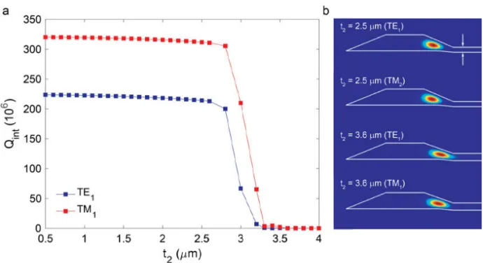
fun-Figure 2.4: Optimization of base silica layer thickness(a) Intrinsic quality factor (Qint) versus base layer thickness (t2, indicated by the arrows inb) of a silica ridge
resonator for the fundamental TE and TM mode families. (b) Calculated mode profiles of the fundamental modes att2= 2.5µm andt2= 3.6 µm
damental TE and the TM mode of the wedge resonator. As the resonator thickness increases, Qintgrows until it starts saturating aroundt1= 8µm. Another interesting
thing to note is that the TM mode has higher Qintthan the TE mode. Such trends of
Qintcan be explained by the fraction of electric field energy contained in the surface
layer. The electric field of thicker resonator modes are more concentrated inside, away from the silica-air boundary, and TM1mode has smaller electric field energy
density at the surface than the TE1mode.
Taking the hint from the wedge resonator results, we choose the total ridge thickness
t1to be 8µm. The top width of the ridge is set to be 20 µm which is large enough to
maintain the high Q of the fundamental modes. While the presence of the base silica layer enables the integration, it can also induce the radiation loss of the resonator. To mitigate the radiation loss, the relative thickness of the base layer (t2 in Figure
2.4) to the total thickness of the ridge (t1) needs to be kept low. Another set of
FEM simulations is performed to find the optimalt2value. The calculated intrinsic
(TM1) is presented in Figure 2.4, where the TE (TM) mode has its electric field
(magnetic field) parallel to the wedge surface. The result shows that ast2increases
from 0.5 µm to 2.5µm, the intrinsic Q degrades by 2.6% and 4.2% for the TE1and
TM1mode, respectively. However, whent2increases above 2.5 µm, a sudden drop
in Q is observed, with Q less than 108 at t2 = 3.1 µm for both modes. The drop
in Q is accounted for by the leakage of the electric field into the base silica layer. The calculated mode profiles of the TE1and TM1mode for the resonator witht2=
2.5 µm and 3.6 µm are shown in Figure 2.4b, revealing the mode leakage for the resonator witht2= 3.6 µm.
While small t2 is beneficial optically, too small value of t2 is undesirable for
me-chanical stability of the silica resonator on silicon. The main issue related to the mechnical stability of the resonator is the buckling of the silica layer that happens when XeF2gas etches the silicon above the threshold undercut value. The buckling
is induced by the thermal stress between the silica and the silicon layer and has been studied previously[47]. Experimentally, it is observed that the threshold undercut value is about 50 µm for a 2.5-µm thick silica resonator. This shows the possibility that the ridge resonator remains unbuckled for silicon undercut of 50 µm away from the optical mode. Such an undercut value is large enough to ensure that the mode does not interact with the silicon substrate. Therefore, we chooset2= 2.5µm as the
base silica layer thickness.
2.4 Design of a single mode silicon nitride waveguide phase-matched to a silica
ridge resonator
A heterogeneous integration of a microresonator with an waveguide of another eator that have the same dimension and are made of the same material. Such a design almost guarantees the ideal phase-matching (i.e., effective-index-matching) which is required for an efficient coupling. The homogeneous integration is also easier in the sense of the required fabrication techniques as the resonator and the waveguide can be simultaneously made in their common process steps. In reality, however, ho-mogeneously integrated resonator-waveguide platforms face a fundamental problem that limits their ultra-high-Q operation.
Problems faced by homogeneous integration of multimode waveguide-resonator
platforms
suffer higher loss (Q−s.s1, Q−cont1 , Q−rad1) due to their small mode area and enhanced electric field at the resonator surface. The inevitable use of multi-mode resonator structures in the highest-Q integrated platforms is usually accompanied by the multi-mode bus waveguides that are phase-matched to the resonators. The multi-multi-mode nature of the bus waveguide becomes the key to the parasitic loss in the waveguide-resonator coupler commonly observed in the homogeneous integration.
A figure of merit that describes the performance of the coupler is the coupling idealityI defined as follows[48, 49].
I = κex,0
κex,0+κp
(2.6)
Here, κex,0 is the external coupling rate of a resonator mode to the target bus
waveguide mode andκpis the parasitic loss given by κp= κrad+Ín>=1κex,nwhere
Í
n>=1κex,n represents the sum of the external coupling rates to the higher order modes. For a device on resonance, the power transmission T can then be expressed as T =
1− 2
K−1+I−1
2 (2.7)
where K = κex,0 / κ0 is the normalized coupling strength and κ0 is the intrinsic
loss rate of the resonator mode. Equation 2.7 shows that for a critical-coupling condition to be reached whereT = 0, the coupling strength should should satisfy
K = Kcrit ≡ 1/(2− I−1). The critical coupling cannot be reached for I ≤ 0.5, and
when I > 0.5, Kcrit as a function of I reaches the minimum Kcrit = 1 at I = 1.
In reality, the ideality I is less than unity because of the parasitic loss. In the case of a multimode bus waveguide, the sum of the external coupling rates to the higher order modes (Í
n>=1κex,n) reduces I, thereby increasingKcrit. As a result, the
external coupling rate between the resonator mode and the fundamental mode of the waveguide must increase in order to achieve the critical coupling. This can be done by reducing the gap between the waveguide and the resonator, or by increasing their interaction length.
adjustments of the multimode waveguide cross-section away from the resonator-waveguide coupler can cause power loss in the higher-order modes of the resonator-waveguide. For example, if inverse tapers are used at the end of the waveguide to enhance the coupling efficiency to the chip, power transferred through the higher-order modes can be completely lost at the inverse tapers. Such power loss degrades the loaded Q of the resonator.
Heterogeneous integration : a single-mode waveguide integrated with a
multi-mode UHQ resonator
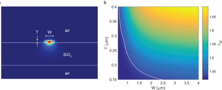
Thus, a single-mode waveguide integrated with a multi-mode ultra-high-Q resonator is a highly desirable platform that avoids the penalty of using a multi-mode waveg-uide. For this end, a waveguide material that has higher refractive index than the resonator material can be chosen. In our case, the waveguide core is made of sil-icon nitride, which has a refractive index of 1.979 at wavelength 1550 nm. It is surrounded by the air cladding at the top and the lateral sides, and it is supported by the silica - air substrate as shown in Figure 2.5a.
A simple way to describe the requirement for a waveguide mode to be formed is using its effective index (neff) defined as neff = β/k where β is the propagation
constant and k is the free-space wavenumber. The effective index of the waveguide mode must satisfy the following condition:
ns < neff < nc (2.8)
Here,nsis the effective index of the slab mode in the base silica layer. We consider
only the fundamental TE slab mode that has the highest effective index among all the slab modes. ns is a function of the thickness of the base layer t2 defined in
the previous section. Fort2 = 2.5 µm, we have ns = 1.42, which is lower than the
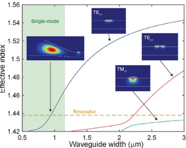
refractive index of silica (1.444). Figure 2.6a shows the calculated effective index of the SiN waveguide modes as functions of the waveguide width (W). In this calculation, the waveguide thickness (T) is set to be 250 nm. Note that atW = 4 µm, the waveguide supports four transverse modes : namely, TE11, TE21, TE31and
TM11(See Figure 2.6b). The polarizations of the TE and the TM mode are parallel
and perpendicular to the top surface of the waveguide, respectively. AsWdecreases,
neff of the higher order modes decreases until it hits the value 1.42 one by one, at
Figure 2.5: Effective index of the TE11mode of the silicon nitride waveguide(a)
Calculated mode profile of the TE11 mode of the SiN waveguide. (b) Calculated
effective index (neff) of the TE11mode as a function of the waveguide width W and
thicknessT denoted ina. The white solid line indicates the pairs (W,T) for which the effective index of the SiN waveguide matches the effective index (1.438) of the TM1 mode of the silica ridge resonator.
only the TE11 mode. Note also that the effective index of the TM1 mode of the
resonator is 1.438 and is indicated in Figure 2.6a. The phase-matching waveguide width is 940 nm at which the waveguide is single-mode.
The color map in Figure 2.5b illustrates the effective index of the TE11 mode for
various values of W and T. The white solid line indicates the pairs (W, T) for which the phase-matching occurs. However, too small or large value ofW on this curve is undesirable because of the high loss induced by the side-wall roughness and the low coupling efficiency due to the large aspect ratio (W:T) of the waveguide, respectively. We chooseW = 940 nmT = 250 nm as our design target.
2.5 Fabrication process
The fabrication process of integrated silica resonators with silicon nitride waveg-uides is schematically shown in Figure 2.7 It begin by growing a thermal silica layer on a (100) prime-grade float-zone silicon wafer. After silicon wafers are loaded into an oxidation furnace (Tystar Tytan 4600), oxidation time is input to the system. The thickness of the thermally grown silica layer can be precisely controlled by the oxidation time[50]. In this work, the oxidation thickness of 8 µm is chosen as discussed in Section 2.3.
Figure 2.6: Design of the single mode SiN waveguide(a) Effective indices of the SiN waveguide modes are plotted as functions of the waveguide width W. The waveguide thicknessT is 250 nm. (b) The calculated mode profiles of low-order modes (TE11, TE21, TE31) for the waveguide with W = 4 µm are shown as inset
layer and patterned using GCA 6300 stepper. Here, together with a disk, align marks are also patterned for the alignment of the wafer and the photomask in the second lithography step taking place later. Then, the silica layer is then wet etched using buffered hydrofluric acid (HF) according to a process used to create wedge resonators[29]. As shown in Figure 2.8a, the resulting etched oxide forms a circular disk structure that defines the exterior of the resonator.
Figure 2.7: Fabrication process for integrated ultra-high-Q microresonator(a) Silica disk is defined on silicon by photolithography and HF etching of an initial silica layer. (b) Thermal oxidation grows a second oxide layer beneath the etched silica disk. (c) PECVD silicon nitride is deposited. (d) Silicon nitride waveguide is defined on silica layer by lithography and etching. (e) Lithography and wet etch of the silica define a ring aperture to the silicon substrate. (f) XeF2etches the silicon
through the ring aperture.
during the final dry etch step below. A lithography/wet-etch step is then used to open an interior, ring aperture to the silicon substrate. In the final step, xenon difluoride (XeF2) etches the silicon through the interior ring aperture so as to create an optical
cavity. The silicon undercut is about 70 µm. The structure of fabricated resonators is shown in Figure 2.8.
2.6 Experimental demonstration of waveguide-resonator coupling
Figure 2.8: Integrated ultra-high-Q microresonator(a) Rendering showing silica ridge resonator with nearby silicon nitride waveguide. Fundamental spatial mode is illustrated in color. (b) SEM image of three ridge resonators with a common silicon nitride waveguide (false red color). White arrows show the direction of circulation within the center resonator for the corresponding direction of coupling from the waveguide. Dashed white box is the region for the zoom-in image in 1d. Dashed white line segment gives the location of cleavage plane used for preparation of the SEM image in 1e. (c) Photograph of a single resonator with endfire coupling provided by a lensed fiber (left) and aspheric lens (right). (d) SEM zoom-in image of the waveguide-resonator coupling region shown within the dashed white box in 1b. (e) SEM image of resonator cross section prepared by cleaving at the dashed white line in 1b.
resonator using a lensed fiber (left) and light collection with an aspheric lens (right). Approximately 25 % of the power could be coupled from the lensed optical fiber to the silicon nitride waveguide. No attempt to improve coupling was made, but in the future a tapered waveguide end can be introduced to improve the coupling efficiency[51]. SEM zoom-in and cross-sectional views are shown in Figure 2.8d and in Figure 2.8e.
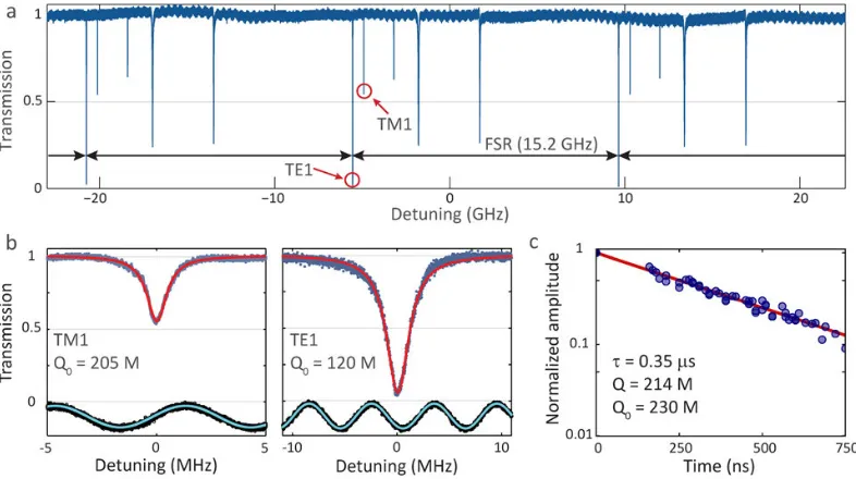
Figure 2.9: Spectral scan of integrated ridge resonator and ring-down measure-ment(a) Spectral scan encompassing two free-spectral-ranges. (b) High resolution zoom-in scan for the TM1 and TE1 modes with intrinsic (Qo) and loaded (Q) quality factors, as well as the linewidth (κ/2π) indicated (M = million). The green
sinu-soidal signal is a frequency calibration scan using a radio-frequency calibrated fiber Mach-Zehnder interferometer (free-spectral range is 5.979 MHz). (c) Superposition of 10 cavity-ringdown signal scans for the TM1 mode with the corresponding decay time and the loaded and intrinsic Q factors.
C h a p t e r 3
DEMONSTRATION OF NONLINEAR OPTICS IN INTEGRATED
ULTRA-HIGH-Q RESONATORS
[1] K. Y. Yang*, D. Y. Oh*, S. H. Lee*, Q.-F. Yang, X. Yi, and K. Vahala. “Bridging ultra-high-Q devices and photonic circuits”. In: arXiv preprint arXiv:1702.05076(2017).
3.1 Abstract
Integrated ultra-high-Q silica ridge resonators combined with performance controls on dispersion and device size enable demonstration of new integrated functionality including soliton generation at electronically-processible rates and high-coherence Brillouin laser oscillation. The device represents a critical advance for miniaturiza-tion of optical-synthesizers[52], optical clocks[9, 53, 54], spectroscopy systems[55– 57], microwave sources[18–21], and rotation sensors[15–17].
3.2 Introduction
69]. They use fiber tapers[49, 70] and prisms[31] for optical coupling. These silica and crystalline-based devices are also the only devices to have so far realized a se-ries of critical functions that include generation of electronic-repetition-rate soliton streams, near-earth-rate rotation measurement, high-performance microwave sig-nal generation and operation as reference cavities and reference sources. These functions are required in a diverse set of new miniature photonic systems and they impose a serious challenge for ultra-high-Q microfabrication through a scalable, integration-ready fabrication process.
As a further complication several functions require performance controls relating to size and dispersion/phase-matching, and these requirements can impose additional demands on the optical Q factor. For example, pulse repetition rates that are both detectable and readily processed by electronics are required in all frequency combs in order to self-reference the comb[71]. To achieve self-referenced octave-span oper-ation in microcombs at practical power levels, frequency comb formoper-ation is divided into a THz-rate comb (micrometer-scale resonator diameter) and an electronics-rate comb (centimeter-scale resonator diameter)[52]. While the smaller-diameter, THz-repetition-rate, soliton combs have been demonstrated with integrated waveg-uides[72, 73], the electronics-rate soliton microcomb has so far only been possible using discrete silica and crystalline devices[27, 28]. Part of the challenge here relates to achieving a high enough Q-factor to overcome the increased pumping volume of the larger electronics-rate soliton comb. Another important consideration is that the soliton mode locking process requires careful resonator design to minimize avoided mode crossings and to create overall anomalous dispersion. Attaining the combined features of ultra-high-Q factor to overcome the large optical pumping volume and resonator-dispersion-management to enable soliton formation while also providing an integrated waveguide has so far not been possible.