Application Note AN-1166
Power Factor Correction using
IR1155 CCM PFC IC
By Helen Ding, Ramanan Natarajan
Table of Contents
IR1155 Detailed Description
PFC Converter Design Procedure using IR1155
For additional data, please visit our website at:
http://www.irf.com
1. Introduction
The IR1155 IC is a fixed frequency PFC IC designed to operate in continuous conduction mode Boost converters with average current mode control. The IC is packed with an impressive array of advanced features such as programmable switching frequency, programmable soft-start, micro-power startup current, user initiated micro-power Sleep mode for compliance with stand-by energy standards, ultra low bias currents for sensing pins. The switching frequency can be programmed from 48KHz to 200Khz. It has very low gate jitter thus eliminating audible noise in PFC magnetics. In addition, dedicated overvoltage protection, cycle-by-cycle peak current limit, open loop protection (OLP) and VCC under voltage lock-out (UVLO). All these features are offered in a compact 8-pin package making IR1155 the most feature-intensive IC for PFC applications. This application note provides an overview of the functionality of IR1155 and demonstrates the design of a universal input 300W AC-DC Boost PFC Converter.
2. IR1155 – Detailed Description
2.1 Overview of IR1155
Fig.1: Typical application diagram of IR1155 based PFC converter
Fig.1 shows the system application diagram of the IR1155 based PFC converter. Only 3 pin functionalities - VFB, COMP & ISNS – are actually needed to obtain the necessary diagnostic signals to achieve power factor correction and maintain output voltage regulation. The functions of the abovementioned 3 pins are as follows:
• VFB – provides DC bus voltage sensing for voltage regulation AC LINE VOUT AC NEUTRAL VCC RTN - + COM 1 OVP 4 VFB 6 VCC 7 GATE 8 ISNS 3 FREQ 2 COMP 5 IR1155S
• COMP – used for compensating the voltage feedback loop to set the correct transient response characteristics
• ISNS – provides sensing of the inductor current, which is used to determine the PFC switch duty cycle
Essentially, there are 2 control loops in the PFC algorithm:
• a slow, outer voltage loop whose function is to simply maintain output voltage regulation
• a fast inner current loop whose function is to determine the instantaneous duty cycle every switching cycle
The current shaping function i.e. power factor correction is achieved primarily by the current loop. The voltage loop is responsible only for controlling the magnitude of the input current in order to maintain DC bus voltage regulation. 2.2 Key Features of IR1155
Programmable Oscillator
The switching frequency of IR1155 is programmed by a capacitor (Cf) that connected to the FREQ pin. The switching frequency can be set from 48KHz to 200KHz with capacitor value from 430pF to 2nF. A 200uA constant current source IOSC(CHG) is used to charge the capacitor voltage from VOSC VAL (2V typ.) to
VOSC PK (4V typ.). Once the voltage on Cf capacitor reaches 4V, the charging
current is disconnected and a 6.6mA discharging current source IOSC(DCHG) is
turned on to discharge Cf capacitor. When Cf voltage is discharged to 2V, the discharging current is discontinued and the charging current source will be turned on again. A sawtooth waveform is presented on FREQ pin as shown in Fig. 2.
Fig.2. FREQ and GATE pin waveforms
(Gate pin demonstrates an example of maximum duty-cycle)
The rising slop of the sawtooth defines the maximum duty-cycle of GATE output, which is demonstrated in Fig.2. In system the actual duty in each switching cycle
is determined by the One Cycle Control modulator, and could vary from minimum 0% to maximum 96%~99%.
The relationship between Cf capacitor and the switching frequency can be found in Fig 3. Higher Cf value results in lower switching frequency.
Fig.3: IR1155 Programmable Switching Frequency
Using capacitor to program frequency improves oscillator noise immunity. It also provides possibility to synchronize IR1155 with external clock. The clock should be a narrow pulse with 1%~5% duty-cycle. The duty-cycle of Sync pulse defines the dead-time of GATE output. 1% Sync duty-cycle results in 99% maximum PFC GATE output. Thus smaller Sync duty-cycle is preferred to achieve lower Total Harmonic Distortion (THD). However keep in mind that the minimum Clock pulse should longer than 100ns to guarantee a reliable operation. The amplitude of Sync signal should higher than VOSC PK.
Fig.4. Sync IR1155 with Ext. signal
(Gate pin demonstrates an example of maximum duty-cycle) 40.00 60.00 80.00 100.00 120.00 140.00 160.00 180.00 200.00 400 650 900 1150 1400 1650 1900 Fr e q u e n c y ( K H z) CT (pF)
Frequency vs. CT
Programmable soft-start
IR1155 facilitates programmability of system soft-start time thus allowing the designer enough freedom to choose the converter start-up times appropriate for the application. The soft start time is the time required for the VCOMP voltage to
charge through its entire dynamic range i.e. 0V through VCOMP,EFF. As a result,
the soft-start time is dependent upon the component values selected for compensation of the voltage loop on the COMP pin – primarily the CZ capacitor
(described in detail in Soft-Start Design section of PFC Converter Design portion of this document). As VCOMP voltage rises gradually, the IC allows a higher and higher RMS current into the PFC converter. This controlled increase of the input current contributes to reducing system component stress during start-up. It is clarified that, during soft-start, the IC is capable of full duty cycle modulation (from 0% to MAX DUTY), based on the instantaneous ISNS signal from system current sensing. Furthermore, the internal logic of the IC is designed to ensure that the soft-start capacitor is discharged when the IC enters the Sleep or Stand-by modes in order to facilitate soft-start upon restart.
User initiated micro-power sleep mode
The IR1155 has an ENABLE function embedded in the OVP/EN pin. When this pin voltage is actively pulled below VSLEEP threshold, the IC is pushed into the
Sleep mode where the current consumption is less than 200uA even when VCC is
above VCC,ON threshold. The system designer can use an external logic level
signal to access the ENABLE feature since VSLEEP threshold is so low. The
IR1155 internal logic ensures that VCOMP is discharged before the IC enters Sleep
mode in order to enable soft-start upon resumption of operation. Protection features
The IR1155 features a comprehensive array of protection features to safeguard the system. These are explained below.
1. Dedicated Overvoltage protection (OVP)
The OVP pin is a dedicated pin for overvoltage protection that safeguards the system even if there is a break in the VFB feedback loop due to resistor divider failure etc. An overvoltage fault is triggered when OVP pin voltage exceeds the VOVP threshold of 106.5%VREF. The IC gate drive is immediately disabled and
held in that state. The overvoltage fault is removed and gate drive re-enabled only when both pin voltages are below the VOVP,RST threshold of 102.2% VREF.
The overvoltage protection level can be programmed through external resistor divider.
2. Open-Loop protection (OLP)
if the VFB pin voltage has not exceeded or has dropped below VOLP threshold of
19%VREF. In the Stand-by mode, all internal circuitry of the IC are biased, the
gate drive is disabled and current consumption is a few milliamps. During start-up, if for some reason the voltage feedback loop is open then IC will remain in Stand-by and not start thus avoiding a potentially catastrophic failure.
3. Cycle-by-cycle peak current limit protection (IPK LIMIT)
The cycle-by-cycle peak current limit is encountered when VISNS pin voltage
exceeds VISNS(PK) threshold of -0.77V (in magnitude). When this condition is
encountered, the IC gate drive is immediately disabled and held in that state until the ISNS pin voltage falls below VISNS(PK). Even though the IR1155 operates
based on average current mode control, the input to the peak current limit comparator is decoupled from the averaging circuit thus enabling instantaneous cycle-by-cycle protection for peak current limitation.
4. VCC UVLO
In the event that the voltage at the VCC pin should drop below that of the VCC
UVLO turn-off threshold, VCC(UVLO) the IC is pushed into the UVLO mode, the gate
drive is terminated, and the turn on threshold, VCC, ON must again be exceeded in
order to re start the process. In the UVLO mode, the current consumption is less than 175uA.
3. PFC Converter Design Procedure
3.1 PFC Converter Specifications
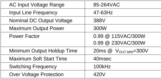
AC Input Voltage Range 85-264VAC
Input Line Frequency 47-63Hz
Nominal DC Output Voltage 388V
Maximum Output Power 300W
Power Factor 0.99 @ 115VAC/300W
0.99 @ 230VAC/300W Minimum Output Holdup Time 20ms @ VOUT,MIN=300V
Maximum Soft Start Time 40msec
Switching Frequency 100kHz
Over Voltage Protection 420V
3.2 Power Circuit Design
Fig.5: IR1155 based PFC Boost Converter Peak Input Current
It is necessary to determine the maximum input currents (RMS & peak) from the specifications in Table 1 before proceeding with detailed design of the PFC boost converter. The maximum input current is typically encountered at highest load & lowest input line situation (300W, 85VAC). Assuming a nominal efficiency of 92% at this situation, the maximum input power can be calculated:
W W P P MIN MAX O MAX IN 326 92 . 0 300 ) ( ) ( = = = η
From this, the maximum RMS AC line current is then calculated:
A V W I PF V P I MAX RMS IN MIN RMS IN MIN MAX O MAX RMS IN 84 . 3 998 . 0 ) 85 ( 92 . 0 300 ) ( ) ( ) ( ) ( ) ( = = = η
The selection of the semiconductor components (bridge rectifier, boost switch & boost diode) is based on IIN(RMS)MAX =3.84A.
Assuming a pure sinusoidal input, the maximum peak AC line current can then be calculated: AC LINE VOUT AC NEUTRAL VCC RTN - + COM 1 OVP 4 VFB 6 VCC 7 GATE 8 ISNS 3 FREQ 2 COMP 5 IR1155S RSNS RSF CSF CIN COUT LBST CZ CP CT Rgm RVFB1 RVFB2 RVFB3 ROVP1 ROVP2 ROVP3 VOUT VCC GND DBST MBST Bridge CVCC RG COM
A V W I V P I MAX PK IN MIN RMS IN MAX IN MAX PK IN 4 . 5 85 ) 326 ( 414 . 1 ) ( 2 ) ( ) ( ) ( ) ( = = = Boost Inductance (LBST)
IR1155 IC is an average current mode controller. An on-chip RC filter is sized to effectively filter the boost inductor current ripple to generate a clean average current signal for the IC. The averaging function in the IC can accommodate a maximum limit of 40% inductor current ripple factor at maximum input current. The boost inductance has to be sized so that the inductor ripple current factor is not more than 40% at maximum input current condition (at peak of AC sinusoid). This is because:
• Higher ripple current factors will interfere with the Average Current Mode operation of One Cycle Control algorithm in IR1155 leading to duty cycle instabilities and pulse skipping which results in current distortion and sometimes even audible noise
• power devices are stressed more with higher ripple currents as the peak inductor current (IL(PK)MAX) also increases proportionately
In this calculation, an inductor current ripple factor of 20% is selected. The ripple current at peak of AC sinusoid at maximum input current is:
A A I I I L MAX PK IN L 1 . 1 4 . 5 2 . 0 2 . 0 ( ) = × = ∆ × = ∆
And, peak inductor current is:
2 1 . 1 4 . 5 2 ) ( ) ( ) ( A A I I I I MAX PK L L MAX PK IN MAX PK L + = ∆ + = A IL(PK)MAX =5.95
In order to determine the boost inductance, the power switch duty cycle at peak of AC sinusoid (at lowest input line of 85VAC) is required.
V V
VIN(PK)MIN = 2× IN(RMS)MIN =120
Based on the boost converter voltage conversion ratio,
69 . 0 388 120 388 V ( ) = − = = V V V D V V D O MIN PK IN O
A kHz V I f D V L L SW MIN PEAK IN BST 1 . 1 100 69 . 0 120 ) ( × × = ∆ × × = H LBST =754µ
A convenient value of 750µH is selected for LBST for this converter.
High Frequency Input Capacitor (CIN)
The purpose of the high-frequency capacitor is to supply the high-frequency component of the inductor current (the ripple component) via the shortest possible loop. This has the advantage of acting like an EMI filter, since it minimizes the high-frequency current requirement from the AC line. Typically a high-frequency, film type capacitor with low ESL and high-voltage rating (630V) is used.
High-frequency input capacitor design is essentially a trade-off between: • sizing it big enough to minimize the noise injected back into the AC line • sizing it small enough to avoid line current zero-crossing distortion (flattening) The high-frequency input capacitor is determined as follows:
F C V kHz A C V r f I k C IN IN MIN RMS IN SW MAX RMS IN I IN L µπ π 24 . 0 85 06 . 0 100 2 84 . 3 2 . 0 2 ( ) ) ( = × × × = × × × = ∆ where:
k∆IL = inductor current ripple factor, of 20% as mentioned earlier
r = maximum high frequency input voltage ripple factor (∆VIN/VIN), assumed 6%
A standard 0.270µF, 630V capacitor is selected for CIN for this converter.
Output Capacitor (COUT)
Output Capacitor design is based on hold-up time requirement
For 20ms hold-up time and minimum output voltage of 300V the output capacitance is first calculated:
2 ) ( 2 ) ( 2 MIN O O O MIN OUT V V t P C − ∆ ⋅ ⋅ = 2 2 ) ( ) 300 ( ) 388 ( 20 300 2 V V ms W COUT MIN − ⋅ ⋅ = F COUT(MIN) =198
µ
Minimum capacitor value must be de-rated for capacitor tolerance (20%) to guarantee minimum hold-up time.
F F C C C TOL MIN OUT OUT
µ
µ
248 2 . 0 1 198 1 ) ( = − = ∆ − =A standard 270µF, 450V capacitor is selected for COUT for this converter.
3.3 IR1155 Control Circuit Design
3.3.1 Current Sense Resistor Design (ISNS pin) In IR1155, there are two levels of current limitation:
- a “soft” current limit, which limits the duty-cycle and causes the DC bus voltage to fold-back i.e. droop
- a cycle-by-cycle “peak” current limit feature which immediately terminates gate drive pulse once the ISNS pin voltage exceeds VISNS,PEAK
“Soft” Current Limit
In IR1155 the COMP pin voltage is directly proportional to the RMS input current into the PFC converter i.e. VCOMP is higher at higher RMS current. Clearly its
magnitude is highest at maximum load PMAX & minimum AC input voltage, VIN,MIN.
The dynamic range of VCOMP in the IC is defined by VCOMP,EFF parameter in the
IR1155 datasheet. Once VCOMP signal saturated (reaches VCOMP,EFF), any system
requirement causing an additional increase in current will cause the IC to respond by limiting the duty cycle and thereby causing the output voltage to droop. This is called “soft” current limit protection. The selection of RSNS must
ensure that “soft” current limit is not encountered at any of the allowable line and load conditions.
RSNS Design
The design of RSNS is performed at the system condition when the inductor
current is highest at lowest input line (VIN,MIN) and highest load (PMAX). Further,
the inductor current is highest at the peak of the AC sinusoid. The duty cycle required at peak of AC sinusoid at VIN,MIN=85VAC in order to regulate VOUT=388V
is: OUT MIN RMS IN OUT PEAK V V V D = − 2 ( ) 69 . 0 385 85 . 2 388 − = = V V V DPEAK
RSNS design should guarantee that
i. PFC algorithm can deliver this duty cycle at peak of AC sinusoid at VIN,MIN &
PMAX condition
ii. soft current limit is encountered whenever there is a further increase in demand for current while operating at VIN,MIN & PMAX condition
DC MIN EFF COMP MAX ISNS g D V V ) 1 ( ) ( ) ( ) ( − ⋅ =
(
)
V V VISNS MAX 0.46 1 . 3 69 . 0 1 6 . 4 ) ( = − ⋅ =Note: if the calculated VISNS(MAX) is higher than the cycle-by-cycle peak
overcurrent limit threshold of the IC, the VISNS(PK) value should be used to
determine RSNS. In this example, VISNS(MAX) is lower than the minimum VISNS(PK)
value that specified in data sheet (0.69V), thus 0.47V is used for RSNS
calculation.
Next the peak inductor current at maximum peak AC line current, derated with an overload factor (KOVL=5%), is calculated.
) 1 .( max ) ( ) (PKOVL LPK OVL IN I K I = + A IIN(PK)OVL =5.95×1.05=6.25
From this maximum current level and the required voltage on the current sense pin, we now calculate the maximum resistor value that can be used for the PFC converter. Ω = = = 074 . 0 25 . 6 46 . 0 , ) ( (max) , MAX SNS OVL PK IN SNS MAX SNS R A V I V R
It is noted that even though IR1155 operates in average current mode it is still safer to use the peak inductor current for current sense resistor design to guarantee avoiding premature fold-back.
Power dissipation in the resistor is now calculated based on worst case RMS input current at minimum input voltage:
S MAX ) RMS ( IN R I R P S = ⋅ 2 W P S R 3.84 (0.074 ) 1.09 2 Ω = =
A standard 70mΩ resistor can be selected for RSNS for the PFC converter.
Peak Current Limit
The cycle-by-cycle peak current limit is encountered when VISNS pin voltage
exceeds VISNS,PEAK. For the PFC converter, this limit is encountered whenever the
A V IPK LMT 11 07 . 0 77 . _ = Ω − =
It is clarified that even though the IR1155 operates based on average current mode control, the input to the peak current limit comparator is decoupled from the averaging circuit thus enabling instantaneous cycle-by-cycle protection for peak overcurrent.
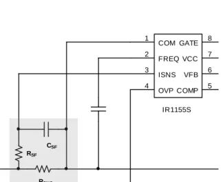
Fig 6: Current Sense Resistor and Filtering
The current sense signal is communicated to the ISNS pin of the IC using a current limiting series resistor, RSF. An external RC filtering for ISNS pin can be
realized (though not necessary for IR1155) by adding a filter capacitor, CSF
between the ISNS pin and COM as shown in Fig.6. A corner frequency around 1-1.5MHz will offer a safe compromise in terms of filtering, while maintaining the integrity of the current sense signal for cycle-by-cycle peak overcurrent protection. SF SF PSF C R f ⋅ ⋅ =
π
2 1With RSF=100Ω, we can use CSF=1000pF to obtain a cross-over frequency of
1.6MHz. The input impedance of the current sense amplifier is approximately 25KΩ. The RSF resistor will form a divider with this 25KΩ resistor. For RSF=100Ω
it is noted that the accuracy of the current sense voltage signal communicated to the IC is more than 99.5%.
3.3.2 Output Regulation Voltage Divider (VFB pin)
The output regulation voltage of the PFC converter is set by voltage divider on VFB pin - RFB1, RFB2, and RFB3. The total impedance of this divider network must
be high enough to reduce power dissipation, but low enough to keep the feedback voltage error (due to finite bias currents into the voltage error amplifier
COM 1 OVP 4 VFB 6 VCC 7 GATE 8 ISNS 3 FREQ 2 COMP 5 IR1155S RSNS RSF CSF
which is less than 0.2uA) negligible. Around 2MΩ is an acceptable value for the total resistor divider impedance.
A standard 499kΩ, 1% tolerance resistor is selected for RFB1 & RFB2 for this
converter. Then, RFB3 is determined based on error amplifier VREF (Typ)=5V and
VOUT=388V converter specification.
) ( ) ( 1 2 3 REF out FB FB REF FB V V R R V R = + Ω = × = V k k RFB 13.03 ) 5.0V -8V 38 ( ) 2 499 ( 0 . 5 3
A standard resistor, RFB3 = 13.0kΩ, 1% tolerance, is selected for this converter.
Power dissipation of divider resistors is given by the following.
(
)
(
1 2)
2 2 2 1 FB FB REF out R R R R V V P P FB FB + − = =(
)
mW k V V P P FB FB R R 73.5 998 2 5 388 2 2 1 × = − = =3.3.3 Dedicated Overvoltage Protection Divider (OVP/EN pin)
IR1155 features a dedicated overvoltage sensing input pin (OVP/EN). User can use the same resistor divider that calculated earlier with FB control. This will give a fixed overvoltage protection level which is 106.5% of regulated output voltage. If a different overvoltage level is desired, a separated OVP resistor divider can be calculated. Here is an example:
Assume standard 499kΩ, 1% tolerance resistor is selected for ROVP1 & ROVP2 for
this converter. The overvoltage protection threshold is 420V: ) 1.065 ( ) ( 065 . 1 1 2 3 REF OV OVP OVP REF OVP V V R R V R × + × = Ω = = V k k RFB 12.8 ) 5.325V -420V ( ) 998 ( 325 . 5 3
The OVP reset point can be calculated:
V V V OV OVPREST 403 065 . 1 022 . 1 × = =
vREF vFB Output Divider H1(s) Error Amplifier + Compensator H2(s) ∆ vm OCC PFC Modulator H3(s) iL Plant G(s) vIN vOUT + _ vREF vFB Output Divider H1(s) Error Amplifier + Compensator H2(s) ∆ vm OCC PFC Modulator H3(s) iL Plant G(s) vIN vOUT vREF vFB Output Divider H1(s) Error Amplifier + Compensator H2(s) ∆ vm OCC PFC Modulator H3(s) iL Plant G(s) vIN vOUT + _
3.3.4 Timing Capacitor (FREQ pin)
The timing capacitor Cf can be obtained per the following formula:
V mA us Fsw Cf 2 194 . 0 ) 45 . 0 1 ( − × =
For 100kHz target switching frequency, Cf is calculated 0.93nF. A standard 1nF capacitor will be used and it programs the switching frequency to 93kHz.
3.3.5 Voltage Loop Compensation (COMP pin)
The voltage feedback loop monitors the DC bus voltage (VOUT) via the VFB
resistor divider whose transfer function is H1(s). Comparison of the VFB pin
voltage and internal reference voltage of the IC by voltage error amplifier yields a control signal (Vm = VCOMP-VCOMP,START). The transfer function of the error
amplifier and compensation network is H2(s). The IR1155 output voltage error
amplifier is a trans-conductance type amplifier and output of the error amplifier is connected to the COMP pin. The control signal directly controls the magnitude of the boost inductor current (IL), which is also the input current of the PFC
converter. The transfer function between IL and control signal Vm is given by
H3(s). The power stage of the PFC converter along with DC bus capacitor,
maintains a constant voltage (VOUT) at the converter output where the system
load draws energy from the converter. The power stage + DC bus capacitor + system load transfer function is given by G(s). The small-signal model of the voltage feedback loop is depicted below in Fig.7. The overall loop gain transfer function T(s) is given by:
T(s) = H1(s).H2(s).H3(s).G(s)
Fig.7: Small-signal modeling of the PFC voltage feedback loop
Voltage loop compensation is performed by adding R/C components between COMP and COM pins in order to:
i. Achieve the appropriate dynamic response characteristics during load/line fluctuations
ii. Ensure that the 2*fAC ripple in VOUT at steady state conditions, does not
cause too much current distortion
In order to evaluate the overall loop gain transfer function T(s), the small-signal transfer function of each of the blocks has to be evaluated first.
Plant Gain, G(s)
The plant gain G(s) models the small signal variation in the DC bus voltage when a small perturbation occurs in the boost inductor current.
G(s) = vOUT/iL = (vOUT/iCHG).(iCHG/iL)
where the small signal parameters are italicized and iL is the boost inductor
current, vOUT is the bus voltage and iCHG is the current sourced at the output of
the boost converter power stage (i.e. boost diode current).
Fig.8: Small-signal model of PFC converter power stage If the system load is a Resistive Load, then the shunt impedance and the system load are in parallel and equal in magnitude hence the equivalent impedance is RL/2. In this case, the transfer function is:
2 1 2 / L out L chg out R sC R i v + =
In the power stage transfer function, this is represented by a pole:
2 2 1 L out PS R C f ⋅ =
π
For a Constant Power Load, the shunt impedance and the system load cancel each other out and the equivalent impedance is infinite, in which case the transfer function reduces to:
COUT RL (2 M IOU T /V O U T ) .... vi (V IN /k M ).... vm v OUT VO U T / IOU T ichg + _ S Y S T E M L O A D COUT RL (2 M IOU T /V O U T ) .... vi (V IN /k M ).... vm v OUT VO U T / IOU T ichg + _ S Y S T E M L O A D
out chg out sC i v 1 =
In the power stage transfer function, this is represented by a pole at the origin. Under a Constant Current Load, since the impedance of a current source is infinitely high, the equivalent impedance is effectively just the shunt impedance:
L out L chg out R sC R i v + = 1
In the power stage transfer function, this is represented by a pole:
L out PS R C f ⋅ =
π
2 1Next (iCHG/iL) transfer function has to be evaluated. Assuming 100% efficiency,
recognize that:
VIN.IL = VOUTIOUT
IOUT is same as the DC component of the boost diode current (ICHG). Hence
VIN.IL = VOUTICHG
Applying linearization and small-signal analysis, for a given DC operating point defined by VIN & VOUT yields the relationship between iCHG & iL:
iCHG/iL = VIN/VOUT
Assuming a resistive load, the overall power stage transfer function can now be written as: 2 1 2 / ) ( L out L OUT IN R sC R V V s G + × = OCC PFC Modulator, H3(s)
In order to derive iL/vm, the One Cycle Control PWM modulator control law is
employed: ) (d M v i R G m L S DC ⋅ ⋅ =
where M(d) = VOUT/VIN for a given DC operating point defined by the DC bus
voltage VOUT and RMS input voltage VIN. This ultimately yields
DC S OUT in m L G R V V v i s H3( )= =
The output divider scales the output voltage to be compared with the reference voltage in the error amplifier.
Therefore: 3 3 2 1 ) ( FB REF FB FB FB OUT R V R R R V = + + OUT REF V V s H1( )=
Error Amplifier & Compensation, H2(S)
The compensation scheme typically employed for a first-order, single-pole system aims to:
• add a pole at the origin in order to increase the low frequency gain and improve DC regulation
• add a low-frequency zero to boost phase margin near cross-over frequency and partially compensate the pole
• add a high-frequency pole to attenuate switching frequency noise and ripple effects
The above 3 requirements can be achieved in case of the transconductance type voltage error amplifier with the compensation scheme shown in Fig.9. However, as mentioned earlier, for the PFC converter, the most important criterion for basing the selection of the compensation component values is the voltage loop bandwidth.
Fig9: Voltage Loop error amplifier compensation network
The error amplifier transfer function is given by:
) C C sR C C ( s ) C sR ( g ) s ( H P Z gm P Z Z gm m + + + ⋅ = 1 2
where gm is the transconductance of the voltage error amplifier. The
-180 -150 -120 -90 -60 -30 0 30 60 90 0.01 0.1 1 10 100 1000 10000 100000 f (Hz) G a in ( d B ) -180 -150 -120 -90 -60 -30 0 30 60 90 P h a s e ( d e g ) EA Gain EA Phase Z gm Z C R f ⋅ ⋅ = π 2 1 0 Cp Cz Cp Cz R f gm P + ⋅ ⋅ = π 2 1 0
The gain and phase of the error amplifier + compensation transfer function is illustrated in Fig.10.
Fig.10: Error Amplifier + compensation transfer function characteristics Voltage Loop Compensation procedure
Step 1: Choose Cz based on soft-start time:
A soft-start time of 40ms is selected. Typical soft start values range from 20ms to a few hundred ms, depending upon the application. The soft-start time represents the time needed by the controller to ramp VCOMP from zero to the
maximum value. The system will take no more than 40ms to achieve near-regulation. ) ( EFF COMP OVEA SS Z V i t C = ⋅
iOVEA and VCOMP(EFF) are taken from the datasheet.
F V A ms CZ µ 0.36µ 9 . 4 44 40 = × =
A standard value of 0.33uF can be selected for the converter for CZ.
Step 2: Choose Rgm to ensure that H1(s).H2(s) attenuation at 2xfAC frequency is
small enough to avoid current distortion:
The amount of 2xfAC ripple on the output capacitor is calculated first. The
minimum fAC of 47Hz is considered here, since the ripple is the maximum at the
lowest AC frequency. The peak-to-zero ripple VOPK is given by:
out O AC MAX in OPK V C f P V ⋅ ⋅ ⋅ ⋅ = 2 2 ,
π
V V V F W V OPK OPK 27 . 5 388 270 47 2 2 326 = ⋅ ⋅ ⋅ ⋅ =µ
π
The peak-to-peak ripple in VOUT is 2xVOPK. This ripple in VOUT is reflected in the
VCOMP voltage based on the attenuation provided by the resistor divider and error
amplifier compensation network combined i.e. H1(s).H2(s) at 2xfAC. The ripple in
VCOMP i.e. ∆VCOMP has to be small compared with the value of the error amplifier
output voltage swing (VCOMP,EFF). Typical values for ∆VCOMP/VCOMP range from
0.5% to 1%. 0.5% is recommended if current shaping has to be excellent while 1% is recommended for higher phase margin and low-oscillation response to load steps. 1% attenuation demands a (GVA) of:
OPK EFF COMP VA V V G ⋅ ⋅ = 2 01 . 0 ) ( dB G V V G VA VA 7 . 46 00465 . 0 27 . 5 2 01 . 0 9 . 4 − = = × × =
This is the required attenuation in H1(s).H2(s) at 2xfAC frequency.
H1(s), given by VREF/VOUT, is next calculated:
dB V V H 0.0129 37.8 388 5 1 = = =−
The required attenuation from H2(s) alone at 2x47Hz is then given by:
36 . 0 9 . 8 1 =− = −H dB GVA
Since the error amplifier pole will be set at a much higher frequency than 2xfAC
(and consequently Cz >> Cp), the error amplifier transfer function at 2xfAC can be
approximated to: Z Z gm m sC ) C sR ( g ) s ( H2 ≅ ⋅ 1+
Since CZ has already been determined, only Rgm needs to be calculated by forcing: 36 . 0 9 . 8 ) 2 ( 1 2 j ⋅ f =G −H =− dB= H π AC VA 2 2 1 2 2 1 ⋅ ⋅ ⋅ − − = Z AC m VA gm C f g H G R π Substituting fAC=47Hz, gm=50µS, CZ=0.33µF yields Ω = k Rgm 5.1
The location of the zero in the compensation scheme can now be estimated: fz = 1/(2*π*Rgm.Cz) = 1/(2*π*5.1kohm*0.33µF) = 95Hz
The location of the pole in the power stage transfer function (assuming a resistive load) is:
fPS = 1/(2*π*COUT*RL/2) = 1/[2*π*270uF*(388V*388V/300W)/2] = 2.3Hz
Step 3: Choose Cp based on high-frequency pole location
The pole frequency should be chosen higher than the cross over frequency and significantly lower than the switching frequency in order to attenuate switching noise and switching frequency ripple in the output capacitor: typical value is 1/6 to 1/10 of the switching frequency. Choosing 1/6xfSW (=0.166*100kHz=16kHz) for
this converter: Cp R Cp Cz Cp Cz R f gm gm P ≅ ⋅ ⋅ + ⋅ ⋅ = π π 2 1 2 1 0 nF kHz k Cp 1.88 166 . 0 100 1 . 5 2 1 = ⋅ ⋅ Ω ⋅ = π
Step 4: Estimate bandwidth & phase margin
The voltage loop response for 85VAC and 264VAC is plotted at full output power condition of 300W in Fig.11. At 85VAC/350W the cross-over frequency is 5Hz and phase margin is about 33°. At 264VAC/350W the cross-over frequency is 16Hz and phase margin is about 23°. This result satisfies the cross-over frequency and phase margin requirements of the design.
Fig.11: Overall Loop Gain at 85/264VAC & 300W (fast loop + low phase margin) For more phase margin discussion and PCB layout guidelines, please refer to IR1152 application note AN-1150.
References
[1] IR1155S datasheet [2] AN-1150 application note
-180 -150 -120 -90 -60 -30 0 30 60 90 -180 -150 -120 -90 -60 -30 0 30 60 90 0.01 0.1 1 10 100 1000 10000 100000 P h a s e ( d e g ) G a in ( d B ) f (Hz)
Gain 85VAC Uncompensated Gain 85VAC Compensated EA Gain
Phase 85VAC Uncompensated Phase 85VAC Compensated EA Phase -180 -150 -120 -90 -60 -30 0 30 60 90 -180 -150 -120 -90 -60 -30 0 30 60 90 0.01 0.1 1 10 100 1000 10000 100000 P h a s e ( d e g ) G a in ( d B ) f (Hz)
Gain 264VAC Uncompensated Gain 264VAC Compensated
EA Gain EA Phase
Phase 264VAC Uncompensated Phase 264VAC Compensated