저작자표시-비영리-변경금지 2.0 대한민국 이용자는 아래의 조건을 따르는 경우에 한하여 자유롭게 l 이 저작물을 복제, 배포, 전송, 전시, 공연 및 방송할 수 있습니다. 다음과 같은 조건을 따라야 합니다: l 귀하는, 이 저작물의 재이용이나 배포의 경우, 이 저작물에 적용된 이용허락조건 을 명확하게 나타내어야 합니다. l 저작권자로부터 별도의 허가를 받으면 이러한 조건들은 적용되지 않습니다. 저작권법에 따른 이용자의 권리는 위의 내용에 의하여 영향을 받지 않습니다. 이것은 이용허락규약(Legal Code)을 이해하기 쉽게 요약한 것입니다. Disclaimer 저작자표시. 귀하는 원저작자를 표시하여야 합니다. 비영리. 귀하는 이 저작물을 영리 목적으로 이용할 수 없습니다. 변경금지. 귀하는 이 저작물을 개작, 변형 또는 가공할 수 없습니다.
Doctoral Dissertation
Improving the Performance and Energy Efficiency of
GPGPU Computing through Adaptive Cache and
Memory Management Techniques
Kyu Yeun Kim
Department of Computer Science and Engineering
Graduate School of UNIST
Improving the Performance and Energy Efficiency of
GPGPU Computing through Adaptive Cache and
Memory Management Techniques
Kyu Yeun Kim
Department of Computer Science and Engineering
Abstract
As the performance and energy efficiency requirement of GPGPUs have risen, memory man-agement techniques of GPGPUs have improved to meet the requirements by employing hardware caches and utilizing heterogeneous memory. These techniques can improve GPGPUs by pro-viding lower latency and higher bandwidth of the memory. However, these methods do not always guarantee improved performance and energy efficiency due to the small cache size and heterogeneity of the memory nodes. While prior works have proposed various techniques to address this issue, relatively little work has been done to investigate holistic support for memory management techniques.
In this dissertation, we analyze performance pathologies and propose various techniques to improve memory management techniques. First, we investigate the effectiveness of advanced cache indexing (ACI) for high-performance and energy-efficient GPGPU computing. Specifically, we discuss the designs of various static and adaptive cache indexing schemes and present im-plementation for GPGPUs. We then quantify and analyze the effectiveness of the ACI schemes based on a cycle-accurate GPGPU simulator. Our quantitative evaluation shows that ACI schemes achieve significant performance and energy-efficiency gains over baseline conventional indexing scheme. We also analyze the performance sensitivity of ACI to key architectural pa-rameters (i.e., capacity, associativity, and ICN bandwidth) and the cache indexing latency. we also demonstrate that ACI continues to achieve high performance in various settings.
Second, we propose IACM, integrated adaptive cache management for high-performance and energy-efficient GPGPU computing. Based on the performance pathology analysis of GPGPUs, we integrate state-of-the-art adaptive cache management techniques (i.e., cache indexing, bypass-ing, and warp limiting) in a unified architectural framework to eliminate performance patholo-gies. Our quantitative evaluation demonstrates that IACM significantly improves the perfor-mance and energy efficiency of various GPGPU workloads over the baseline architecture (i.e., 98.1% and 61.9% on average, respectively) and achieves considerably higher performance than the state-of-the-art technique (i.e., 361.4% at maximum and 7.7% on average). Furthermore, IACM delivers significant performance and energy efficiency gains over the baseline GPGPU ar-chitecture even when enhanced with advanced architectural technologies (e.g., higher capacity, associativity).
Third, we propose bandwidth- and latency-aware page placement (BLPP) for GPGPUs with heterogeneous memory. BLPP analyzes the characteristics of a application and determines the optimal page allocation ratio between the GPU and CPU memory. Based on the optimal page allocation ratio, BLPP dynamically allocate pages across the heterogeneous memory nodes. Our
experimental results show that BLPP considerably outperforms the baseline and state-of-the-art technique (i.e., 13.4% and 16.7%) and performs similar to the static-best version (i.e., 1.2% difference), which requires extensive offline profiling.
Contents
I Introduction . . . 1
II Background . . . 6
2.1 Baseline GPGPU Architecture . . . 6
2.2 Performance Pathologies of GPGPU Caches . . . 6
2.3 Heterogeneous Memory Systems . . . 7
III Quantifying the Performance and Energy Efficiency of Advanced Cache Indexing for GPGPU Computing . . . 9
3.1 Motivation . . . 9
3.2 Static Cache Indexing . . . 10
3.3 Adaptive Cache Indexing . . . 12
3.4 Evaluation . . . 17
IV Improving the Performance and Energy Efficiency of GPGPU Computing through Integrated Adaptive Cache Management . . . 30
4.1 Motivation . . . 30
4.2 The IACM Architecture . . . 30
4.3 Evaluation . . . 39
V BLPP: Improving the Performance of GPGPUs with Heterogeneous Memory through Bandwidth- and Latency-Aware Page Placement . . . 57
5.2 Design and Implementation . . . 57 5.3 Evaluation . . . 61 VI Related Work . . . 68 VII Conclusions . . . 71 References . . . 73 Acknowledgements . . . 80
List of Figures
1 The baseline GPGPU architecture . . . 6
2 GPGPU with heterogeneous memory . . . 7
3 An example of cache conflicts when runningATAX . . . 9
4 Bitwise XOR indexing . . . 10
5 Polynomial modulus indexing . . . 11
6 The overall execution flow of the adaptive cache indexing scheme . . . 13
7 An example of determining a victimized bit . . . 13
8 An example of selecting a new indexing bit . . . 14
9 An example of cache-line state transitions . . . 16
10 Overall performance results of the ACI schemes applied to the L1 data cache . . 19
11 Overall energy results of the ACI schemes applied to the L1 data cache . . . 20
12 Execution cycle breakdown of the conventional and ACI schemes applied to the L1 data cache . . . 21
13 L1 data cache misses and reservation fails of the conventional and ACI schemes applied to the L1 data cache . . . 21
14 Energy consumption breakdown of the conventional and ACI schemes applied to the L1 data cache . . . 22
15 Power consumption breakdown of the conventional and ACI schemes applied to the L1 data cache . . . 23
16 Execution cycle breakdown of the conventional and ACI schemes applied to the
L1 data and L2 caches . . . 24
17 L2 data cache misses and reservation fails of the conventional and ACI schemes applied to the L1 data and L2 caches . . . 24
18 Energy consumption breakdown of the conventional and ACI schemes applied to the L1 data and L2 caches . . . 25
19 Power consumption breakdown of the conventional and ACI schemes applied to the L1 data and L2 caches . . . 26
20 Sensitivity to the indexing latency . . . 27
21 Sensitivity to the L1 data cache associativity and capacity . . . 28
22 The baseline GPGPU architecture augmented with IACM . . . 31
23 The overall execution flow of IACM . . . 32
24 The overall execution flow of ADI . . . 33
25 IACM design space exploration . . . 42
26 Performance comparison of the three IACM designs . . . 43
27 Overall performance and energy results . . . 44
28 Performance and energy breakdowns of the streaming benchmarks . . . 46
29 Performance and energy breakdowns of the conflicting benchmarks . . . 48
30 Performance and energy breakdowns of the thrashing benchmarks . . . 49
31 Performance and energy breakdowns of the conflicting and thrashing benchmarks 50 32 Performance and energy breakdowns of the cache-friendly benchmarks . . . 51
33 Performance and energy results of different combinations of the advanced cache management techniques . . . 52
34 Performance comparison with the state-of-the-art technique . . . 52
35 Sensitivity of the performance gain of IACM to architectural parameters . . . 54
36 Sensitivity of the energy-efficiency gain of IACM to architectural parameters . . . 55
37 Overall architecture of BLPP . . . 57
38 Overall performance results . . . 63
39 Execution cycle breakdowns . . . 64
40 GPU memory allocation ratio . . . 65
List of Tables
1 Architectural parameters of the simulated system . . . 17
2 Benchmarks . . . 18
3 Hardware overheads of the IACM components for the baseline GPGPU architec-ture with 16 SIMT cores . . . 38
4 Simulation parameters . . . 40
5 Benchmarks . . . 41
6 Simulation parameters . . . 62
I
Introduction
From big data computing to machine learning, GPGPUs are being used in various computing domains as it utilizes thousands of cores for high performance and energy-efficient computing. To further improve the performance and energy efficiency, modern GPGPUs have begun to improve memory management techniques in terms of both architecture and system software. For the GPGPU architecture, hardware caches have been widely adopted in the memory hierarchy [1, 2] for faster memory access. For example, the NVIDIA Kepler GK110 architecture includes 16KB (or 48KB) L1 cache per core and total capacity of 1,536KB L2 caches [1]. The rationale behind this design decision is that small yet fast GPGPU caches would effectively capture the locality in the memory accesses of GPGPU workloads and reduce memory access overhead, similarly to CPU caches.
However, incorporating hardware caches in the GPGPU memory hierarchy does not always guarantee enhanced performance and energy efficiency in GPGPU computing. The fundamental limitation is that in GPGPU, thousands of GPGPU threads share significantly small capacity of GPGPU caches, which can cause various performance pathologies. Without effective cache management, GPGPU architectures may fail to achieve the best possible performance and energy efficiency when using GPGPU caches.
In order to improve effectiveness of hardware caches, researchers have proposed architectural techniques based on adaptive warp scheduling and limiting [3–8], and cache bypassing [4, 5]. Relatively little work, however, has been done in the context of advanced cache indexing (ACI) for GPGPUs, which has been shown to be one of the most effective techniques to improve performance in CPU hardware caches [9–11].
To bridge this gap, we investigate the effectiveness of advanced cache indexing for high per-formance and energy efficient GPGPU computing [12, 13]. We discuss the design of various static and adaptive cache indexing schemes and present implementation for GPGPU architec-tures. We then quantitatively evaluate the static and adaptive cache indexing schemes compared to the baseline conventional indexing scheme in terms of performance and energy efficiency us-ing GPGPU workloads. We also investigate the performance sensitivity of the advanced cache indexing schemes to key architectural parameters such as cache capacity and indexing latency.
Furthermore, little work has been done to create a unified architecture framework that tightly integrates the state-of-the-art adaptive cache management techniques and investigate their ef-fectiveness when they are tightly integrated. Based on the analysis of GPGPU performance pathologies, we conclude that multiple cache management schemes needs to be integrated to achieve the best possible performance. Therefore, we propose IACM [14, 15], integrated adap-tive cache management for high-performance and energy-efficient GPGPU computing. IACM incorporates the state-of-the-art adaptive cache management techniques (i.e., adaptive cache indexing, adaptive warp limiting, and cache bypassing) in a unified architectural framework. Based on a cycle-accurate GPGPU simulator [16] and various GPGPU workloads, we quantify
the performance and energy efficiency of IACM.
In terms of system software, GPGPUs have begun to utilize heterogeneous memory for im-proved performance. Researchers [17–23] have presented the design and implementation of vir-tual memory for GPGPUs with heterogeneous memory that comprises the GPU (e.g., GDDR5) and CPU (e.g., DDR4) memory nodes. By using both GPU and CPU memory nodes, GPGPUs are able to increase effective bandwidth and capacity of the memory. For better heterogeneous memory system, system must provide the transparent support for virtual memory so that pro-grammers can fully utilize all the available heterogeneous memory nodes without the need for manually managing the data transfers.
In order to achieve the best possible performance on GPGPUs with heterogeneous memory, system should first dynamically categorize application characteristics. Then, it should allocate pages judiciously across the heterogeneous memory nodes by considering the application char-acteristics and the differences between GPU and CPU memory in terms of both bandwidth and latency. Most of the aforementioned prior works have only investigated the efficient design and implementation of the address translation [20,21], cache hierarchy [19], and warp scheduling [18], lacking the heterogeneity-aware memory management.
The prior work in GPGPUs with heterogeneous memory [17] has proposed a memory man-agement technique that places memory pages by considering the memory bandwidth difference of the GPU and CPU memory. However, it lacks the consideration of the GPGPU caches, which significantly affect the memory performance in terms of bandwidth and latency. This leads to al-locating pages across the heterogeneous memory nodes in a latency-oblivious manner, achieving suboptimal performance.
To bridge this gap, we propose bandwidth- and latency-aware page placement (BLPP) for GPGPUs with heterogeneous memory which consists of three phases [24]. First, BLPP col-lects the performance counter data of the target application using offline profile data or using runtime information. Second, BLPP determines the optimal memory allocation ratio based on the application characteristics and the performance differences of the heterogeneous memory nodes. Finally, it dynamically allocates memory pages based on the optimal allocation ratio. We demonstrate the effectiveness of BLPP through quantitative evaluation with various GPGPU workloads.
Specifically, this dissertation makes the following contributions: • Analysis on Advanced Cache Indexing Schemes
– We explain performance pathologies of GPGPU hardware cache by analyzing memory access pattern of GPGPU application and discuss various static and adaptive cache indexing schemes that can mitigate the issues. We discuss design and implementa-tions of advanced cache indexing schemes for high performance and energy-efficient GPGPU computing.
– With a cycle-accurate GPGPU simulator [16], we provide a quantitative evaluation of the advanced cache indexing schemes. We use benchmarks from various bench-mark suites with a wide range of memory access characteristics for in-depth analysis. Specifically, we quantify the performance and energy efficiency of the advanced cache indexing schemes for the L1 data and L2 caches of the GPGPU architecture. We provide various data such as cycle breakdown, reservation fails, and miss rate to gain a deeper insight.
– We investigate the performance sensitivity of the advanced cache indexing schemes to key architectural parameters: indexing latency, number of sets, associativity, and capacity of L1 data cache. Our sensitivity study demonstrates that the advanced cache indexing schemes continues to provide significant performance gains even when the additional indexing latency occurs due to the hardware complexity. And even when the advanced cache indexing schemes are used in a hardware cache that is en-hanced with larger capacity or high associativity, it will continue to provide significant performance gains.
• Propose and Evaluate Integrated Adaptive Cache Management
– We propose IACM, integrated adaptive cache management for high performance and energy-efficient GPGPU computing. IACM is an integrated GPGPU architecture that incorporates the state-of-the-art adaptive cache management techniques (i.e., adaptive cache indexing, adaptive warp limiting, and cache bypassing) in an unified manner.
– We present three IACM designs, each with a different methods of unifying adaptive cache management techniques. We perform extensive design parameter sweeps to find parameters with the best performance for each of three IACM designs based on a cycle-accurate GPGPU simulator. We then compare performance of three IACM designs and determine the design that provides the highest performance among the three.
– We quantify the performance and energy efficiency of IACM using the IACM design with the best performance. Our quantitative evaluation demonstrates that IACM significantly outperforms the baseline GPGPU architecture in terms of performance and energy efficiency (i.e., 98.1% and 61.9% on average) by effectively unifying the adaptive cache management techniques in an integrated manner and eliminating the performance pathologies.
– We quantitatively compare IACM with the state-of-the-art technique [6] which also integrates various cache management techniques. Our experimental results show that IACM outperforms the state-of-the-art technique with a majority of the evaluated benchmarks. This is because IACM employs the adaptive cache indexing technique
unlike state-of-the-art which employs the static cache indexing technique, and applies the adaptive techniques in a more coordinated manner. Overall, IACM achieves considerably higher performance (i.e., 361.4% at maximum and 7.7% on average) than the state-of-the-art technique across all the 20 evaluated benchmarks, which clearly demonstrate the effectiveness of IACM.
• Propose and Evaluate Bandwidth- and Latency-aware Page Placement
– We identify and quantify that the state-of-the-art page placement technique [17] achieves suboptimal performance on the practical GPGPU architecture with het-erogeneous memory. We analyze that this is mainly because the prior technique lacks the consideration of the performance effects of the GPGPU caches in terms of bandwidth and latency.
– We propose BLPP, bandwidth- and latency-aware page placement for GPGPUs with heterogeneous memory. BLPP is comprised of three phases. First, BLPP collects the performance characteristics (e.g., cache miss rates and memory traffic) of the target application using offline profile data or runtime information. Second, it determines the optimal allocation ratio across the heterogeneous memory nodes based on the application characteristics. Finally, it dynamically places memory pages by using the optimal allocation ratio determined from previous phase.
– We propose and evaluate two versions of BLPP. The static version of BLPP (S-BLPP) employs the offline profile data of the target application. In contrast, the dynamic version of BLPP (D-BLPP) dynamically classifies the target application character-istics and determines the optimal allocation ratio without requiring offline profiling. Using quantitative evaluation, we show that D-BLPP achieves similar performance to S-BLPP.
– We quantify the effectiveness of BLPP based on a cycle-level GPGPU simulator and a variety of GPGPU workloads. Our experimental results show that BLPP considerably outperforms (e.g., 16.7% higher performance) the state-of-the-art technique [17] and achieves the performance similar (e.g., 1.2% lower performance) to that of the static best version, which requires extensive offline profiling for every application, dataset, and memory allocation ratio. We also provide execution cycle breakdown and memory allocation ratio data of each techniques for an in-depth analysis.
The rest of this dissertation is organized as follows. Section II provides background informa-tion on the baseline GPGPUs and its performance pathologies. Secinforma-tion III provides performance and energy efficiency analysis on GPGPUs when using advanced cache indexing schemes. Sec-tion IV presents the IACM architecture and compares its performance and energy efficiency against the baseline and state-of-the-art architecture. Section V presents BLPP and compares
its performance to the baseline and state-of-the-art technique. Section VI summarizes related works and Section VII concludes the dissertation.
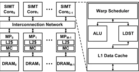
Interconnection Network SIMT Core0 SIMT Core1 SIMT CoreC-1 DRAM0 MC L2$ MP0 MC L2$ MPM-1 ALU LDST Warp Scheduler L1 Data Cache DRAMM-1 DRAM1 MC L2$ MP1
Figure 1: The baseline GPGPU architecture
II
Background
2.1 Baseline GPGPU Architecture
Figure 1 shows the baseline GPGPU architecture that consists of multiple single-instruction multiple-thread (SIMT) cores1. Each SIMT core includes L1 memory components such as a private L1 data cache, which serves memory requests from LDST unit. When a cache miss occurs from L1 data cache, memory request is sent to the corresponding memory partition through the interconnection network. Each memory partition consists of hardware components such as an L2 cache bank, and a memory controller and is connected to an off-chip DRAM module. To support outstanding memory requests, L1 and L2 caches are augmented with the miss status holding registers (MSHRs), which dynamically track the status of pending misses.
A GPGPU program consists of kernels that are offloaded to GPGPUs. These kernels can be divided into concurrent thread blocks (CTA), warps, and threads. Threads belonging to the same CTA can be synchronized using synchronization primitives such as barriers and share data through a shared memory. With CTA being consisted of multiple warps, group of threads form a single warp. SIMT core executes threads in a warp granularity, and every thread within a scheduled warp executes in a lockstep manner. Execution order of warps can affect overall performance of GPGPU. Therefore, prior works have extensively investigated warp scheduling techniques such as Greedy-Then-Oldest (GTO) [3] and two-level [8] scheduling techniques.
2.2 Performance Pathologies of GPGPU Caches
Similar to CPU caches, GPGPU caches may suffer from well-known performance pathologies such as thrashing and contention. In GPGPU computing, cache thrashing occurs when the working-set size of a kernel exceeds the capacity of the cache. One of the key parameters that
1
GPU
High-Bandwidth GPU Memory
CPU
Medium-Bandwidth Large CPU Memory
GPU-CPU Link
Figure 2: GPGPU with heterogeneous memory
determines the effective working-set size of a kernel is number of active warps, which is controlled by the warp scheduler. GPGPUs are significantly more vulnerable to cache thrashing than CPUs due to thousands of threads sharing the cache.
Cache contention occurs when concurrent threads compete for hardware resources required for a cache operation. In GPGPU computing, the hardware resources that often trigger drastic performance degradation from contention are cache lines, MSHR entries, and miss queue entries. Areservation failoccurs when a memory operation cannot proceed because of a failure to reserve any of the aforementioned hardware resources.
Specifically, a cache-line reservation fail for a memory operation occurs when all the cache lines in the set associated with the memory operation are currently reserved for other pending memory operations. With ineffective cache indexing, cache-line reservation fails can frequently occur even when there are plenty of available cache lines. Reservation fails for MSHR and miss queue entries typically occur with frequent cache misses.
Threads that cause cache contention or cache thrashing can belong to a same warp or dif-ferent warps. Following the terminologies used in [3], we refer to the former as the intra-warp interference and the latter as the inter-warp interference. Reason we are distinguishing intra-warp and inter-intra-warp interferences is because different cache management technique should be used to mitigate performance pathologies depending on the interference, which will be discussed in the later sections.
2.3 Heterogeneous Memory Systems
To date, high-performance GPGPUs have been mostly managed as separate computing devices from CPUs, requiring GPGPU programmers to manually manage memory transfer between the GPU and CPU memory. Therefore, programmers had to decide which and when memories should be transferred between the GPU and CPU memory for optimal performance. To enhance the programmability and support a wide range of applications, researchers have extensively investigated automatic memory management techniques to provide the unified address space for GPGPUs with heterogeneous memory that comprises the GPU and CPU memory nodes [17, 19, 20, 22, 23, 25].
Figure 2 shows the GPGPU architecture with heterogeneous memory, which enables the GPGPU to seamlessly access the data in the GPU and CPU memory nodes without manual memory management by a programmer. In line with the state-of-the-art designs, we assume that the CPU and GPGPU are connected via a dedicated high-performance GPU-CPU link such as NVIDIA’s NVLINK [26] and AMD’s HyperTransport [27].
Prior works have presented the design and implementation of the OS-controlled unified mem-ory for GPGPUs with heterogeneous memmem-ory [19, 20, 25]. In this work, we follow the work [19] and assume that the underlying GPGPU architecture with heterogeneous memory implements theselective cachingprotocol. Reason we are implementing selective caching is mainly because the selective caching protocol achieves high performance with low hardware complexity. In contrast, the other proposals require intrusive modifications in the GPU and/or CPU memory hierarchy [20, 25], significantly increasing the hardware complexity.
The selective caching protocol disallows the GPGPU caching of any data that is (1) mapped in the CPU physical memory or (2) actively used by the CPU on-chip caches. By enforcing these properties, the selective caching protocol eliminates the need for supporting cache coherence in the GPGPU caches and requires no or little modifications in the GPU and CPU memory hierarchy [19].
Listing 1: The code snippet of theATAX benchmark v o i d a t a x _ k e r n e l 1 ( f l o a t ∗A, f l o a t ∗x , f l o a t ∗tmp ) { // blockDim . x = 256 i n t i = b l o c k I d . x∗blockDim . x + t h r e a d I d . x ; i f ( i < NX) { i n t j ; // NY = 4096 f o r ( j =0; j < NY; j ++) tmp [ i ] += A[ i ∗ NY + j ] ∗ x [ j ] ; } }
Block offset
7
0
TID in warp
19
14
j
2
Figure 3: An example of cache conflicts when running ATAX
III
Quantifying the Performance and Energy Efficiency of
Ad-vanced Cache Indexing for GPGPU Computing
3.1 Motivation
The baseline GPGPU architecture is potentially vulnerable to cache thrashing and contention given that thousands of threads share small hardware caches. To gain a deeper understanding of the cache performance pathology of GPGPUs, we present a case study with theATAXbenchmark in the PolyBench benchmark suite [28], which contains a pathological memory access pattern.
Listing 1 shows the code snippet of ATAX. Because NY is 4096, the memory addresses for concurrent accesses to arrayAperformed by all 32 threads within a warp have unique bit values from B14 to B18, which essentially encode the thread ID in a warp (see Figure 3). Thus, the bits fromB14to B18are highly effective for avoiding reservation fails and conflict misses among
the threads within a warp.2 In contrast, because every thread in a warp executes in a lock-step manner, the bits fromB7 to B13, determined by the variable j, have identical values across all
threads within a warp. Therefore, the bits fromB7 toB13are ineffective if used to mitigate the cache thrashing among the threads.
2
Note that a reservation fail occurs when there is no available cache line or hardware resource (MSHR or miss queues) for a memory request because all of them are currently in use to serve other pending memory requests.
B
S
S
0
N-1
Figure 4: Bitwise XOR indexing
With a hardware cache that consists of 32 sets (i.e., indexing bits consist of five bits), the conventional cache indexing scheme employs the bits from B7 to B11, causing drastic cache contention among the threads in the same warp. If the cache employs an advanced cache indexing scheme that can avoid this cache contention, the overall performance can be significantly improved. For instance, adaptive cache indexing can indicate that the bits fromB14to B18 are highly effective for avoiding cache contention based on runtime information, therefore using employ them as the indexing bits.
The cache thrashing and contention of GPGPU workloads can be triggered by intra-warp
interference andinter-warpinterference [3]. While inter-warp interference can be mitigated using other GPGPU cache management techniques, such as warp scheduling [3], they are generally ineffective when used to address intra-warp interference. Because advanced cache indexing is expected to efficiently address both types of interference, it is crucial to thoroughly investigate the effectiveness of various advanced cache indexing schemes for high performance and energy efficient GPGPU computing.
3.2 Static Cache Indexing
This section discusses advanced static cache indexing schemes. In Sections 3.2 and 3.3, without a loss of generality, we assume a GPGPU architecture with an N-bit address space. We also assume a hardware cache whose block size, associativity, and number of sets are correspondingly
2B bytes,W, and2S. AnN-bit memory address A is expressed as A[N−1 : 0]and its cache-block addressAB is expressed asA[N−1 :B]. In addition, cache indexI for a memory address is expressed asI[S−1 : 0].
3.2.1 Bitwise XOR Indexing
Bitwise XOR indexing (BXI) computes the set index mapped to a cache-block address by per-forming the bitwise XOR operation for the first and second lowest S bits of the cache-block address [10]. Lowest 2S bits are used to construct a set index because the lower bits change more frequently than the higher bits in a typical sequence of memory accesses, resulting in a more uniform distribution of the memory addresses during a time interval. Figure 4 shows how BXI constructs the indexing bits for an N bit memory address. Owing to its simple and rapid hardware implementation, BXI is applicable to L1 caches. In addition, the area overhead of BXI
I5 =A30⊕A29⊕A28⊕A27⊕A24⊕A22⊕A18⊕A17⊕A12 I4 =A31⊕A29⊕A28⊕A27⊕A26⊕A23⊕A21⊕A17⊕A16⊕A11 I3 =A30⊕A28⊕A27⊕A26⊕A25⊕A22⊕A20⊕A16⊕A15⊕A10 I2 =A29⊕A27⊕A26⊕A25⊕A24⊕A21⊕A19⊕A15⊕A14⊕A9 I1 =A28⊕A26⊕A25⊕A24⊕A23⊕A20⊕A18⊕A14⊕A13⊕A8 I0 =A31⊕A30⊕A29⊕A28⊕A25⊕A23⊕A19⊕A18⊕A13⊕A7
Figure 5: Polynomial modulus indexing
is expected to be low because it requires 5 XOR gates in the case of the 4-way 16KB L1 data cache with a block size of 128 bytes.
3.2.2 Reverse-Engineered Bitwise XOR Indexing
Recent work has reverse-engineered the NVIDIA GTX470 architecture and concluded that a variant of the bitwise XOR indexing scheme appears to be employed in its L1 data cache [29]. Specifically, as for the 4-way 16KB L1 data cache with a block size of 128 bytes, the reverse-engineered bitwise XOR indexing (RXI) scheme computes the indexing bits as follows – I4 = A19⊕A11,I3=A17⊕A10,I2 =A15⊕A9,I1 =A14⊕A8, and I0 =A13⊕A7 [29].
The area overhead of RXI is expected to be low because RXI requires the same number of the XOR gates to compute the indexing bits for the same cache configuration as BXI does. The main difference between BXI and RXI is that RXI employs higher bits to construct some of the indexing bits (e.g., A19 for I4). We conjecture that the design decision of RXI has been made
mainly based on the observation that some of the higher bits can effectively reduce the cache contention for some GPGPU workloads. Section 3.4 quantitatively compares the performance and energy efficiency outcomes of BXI and RXI.
3.2.3 Polynomial Modulus Indexing
Polynomial modulus indexing (PLI) represents an N-bit memory address as a polynomialA(x)
in the Galois field of 2 (GF(2)) [6,7,9,10]. For instance,A(x)for memory address 57 is expressed asx5+x4+x3+ 1. Suppose thatP(x)is a polynomial whose order isS. A(x) can be expressed asA(x) =P(x)·Q(x) +R(x) whereQ(x)and R(x) are polynomials in GF(2) and the order of
R(x) is less thanS. In such a case,R(x) can be considered as the polynomial representation of the cache index for the memory address [6]. In other words, cache index R(x) is computed as
R(x) =A(x) mod P(x).
Prior work holds that PLI can achieve the best permutation when P(x) is an irreducible polynomial [9]. For example, we assume a cache with 64 sets (i.e.,S = 6) and 128-byte blocks
(i.e., B = 7). We also assume P(x) =x6+x+ 1, which is one of the irreducible polynomials whose order is 6. Figure 5 shows the indexing bits constructed by PLI for the aforementioned cache, whose configuration is identical to that of the L2 cache evaluated in Section 3.4.
PLI near-randomly interleaves consecutive memory addresses with various strides, even when the stride is a multiple of the number of cache sets (i.e.,2S) [6,9]. However, prior work states that PLI is not resistant to all possible memory strides, potentially leading to suboptimal performance in pathological cases (e.g., when the stride is 2S−1) [11]. Furthermore, because the hardware logic required to compute the index is rather complicated (e.g., trees of XOR gates) and is in the critical path, PLI may increase the hit time of the cache [30]. We investigate the performance impact of the additional indexing latency in Section 3.4. The area overhead of PLI is expected to be rather low (but slightly higher than BXI and RXI) because it requires tens of XOR gates to compute the indexing bits, as shown in Figure 5.
3.2.4 Prime Modulo Indexing
Prime modulo indexing (PRI) computes the index of a cache block address (AB) using the following equation: I = AB modp, where p is the largest prime number that is equal to or smaller than the number of sets in the cache [11, 31]. The main advantage of PRI is that it is resistant to a wide range of memory strides, even including the aforementioned pathological cases for PLI [11].
However, given that PRI requires an integer division to compute the index for each cache access, it can introduce a significant indexing latency, potentially degrading the overall perfor-mance. While prior work proposed a fast implementation for PRI [11], it applied PRI only to the L2 cache because the additional indexing latency of PRI makes it infeasible for L1 caches. In addition, PRI is associated with from the set fragmentation problem [11], in which some of the sets in the cache are unutilized if the number of sets is not a prime number, which is a common case (e.g., a power of two). For instance, if a hardware cache consists of 32 sets, PRI only utilizes 31 sets, resulting in set fragmentation of 3.125% (= 321 ×100).
3.3 Adaptive Cache Indexing
With regard to adaptive cache indexing (ADI) for GPGPUs, we adopt a technique referred to as ASCIB, that has been proposed to adjust the cache indexing bits dynamically to reduce conflict misses for CPU caches [32]. We choose ASCIB as the baseline design owing to its simplicity and applicability to L1 caches.
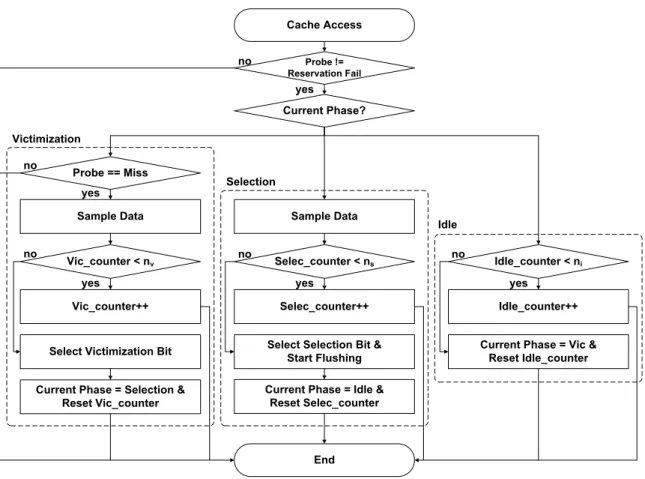
The ADI phase consists of three phases: victimization, selection, and idle phases (Figure 6). Thevictimization phase determines the victim bit from among the current indexing bits, which contributes the least to reducing set conflicts. For this purpose, ADI computes the entropy of each of the current indexing bits to quantify its variability. The entropy counter (CE) of each indexing bit increments by 1, if the corresponding indexing bit value is 1. Assuming that the
Probe != Reservation Fail Current Phase? Cache Access Vic_counter < nv Sample Data Probe == Miss Sample Data Selec_counter < ns Vic_counter++
Select Victimization Bit
Selec_counter++ Select Selection Bit &
Start Flushing
Idle_counter < ni
Idle_counter++ Current Phase = Vic &
Reset Idle_counter Victimization Selection Idle End yes
yes yes yes
no no no
no
yes no
Current Phase = Idle & Reset Selec_counter Current Phase = Selection &
Reset Vic_counter
Figure 6: The overall execution flow of the adaptive cache indexing scheme B2B1B0 0 0 1 0 1 1 0 0 1 0 1 0 entropy(B0)=MIN(3,4-3)=1 corr(B0,B1)=MAX(3,4-3)=3 entropy(B1)=MIN(2,4-2)=2 corr(B0,B2)=MAX(3,4-3)=3 entropy(B2)=MIN(0,4-0)=0 corr(B1,B2)=MAX(2,4-2)=2 Figure 7: An example of determining a victimized bit
total sample count isT, the entropy of each indexing bit is computed to beM IN(CE, T−CE). In addition, ADI computes the correlation of every pair of the current indexing bits. The correlation counter (CC) increments by 1 if the indexing bits in the corresponding pair have the same value. The correlation of each pair is computed to beM AX(CC, T −CC).
ADI employs a metric calledusefulnessto compare the entropy of each of the indexing bits and the correlation of each pair of the indexing bits directly. With a total sample count of T, the usefulness of the entropy (i.e., E) of each of the indexing bits is computed to beE and the usefulness of the correlation (i.e.,C) of each pair of the indexing bits is computed to beT −C. If the indexing bit with the lowest entropy has a lower usefulness value than the pair of the two indexing bits with the highest correlation, the indexing bit with the lowest entropy is selected as the victim bit. Otherwise, the indexing bit that has lower entropy between the two indexing
Candidates B2B1 0 0 1 0 0 1 0 1 1 1 Index B0 1 1 0 1 0 B2 B1 B2 B1 0 1 0 0 1 1 1 0 0 1 MRP(B2)=(MP0(B2)+MP1(B2))/2=1 MP0(B2)=2/2: 01 MP1(B2)=3/3: 010 MRP(B1)=(MP0(B1)+MP1(B1))/2=7/4 When B0=0 When B0=1 When B0=0 When B0=1
MP0(B1)=2/1: 11 MP1(B1)=3/2: 001
Figure 8: An example of selecting a new indexing bit
bits with the highest correlation is selected as the victim bit. Figure 7 shows an example of the determination of a victimized bit (i.e.,B2). In this work, the victimization phase period is configured as 1K L1 data cache misses.
The hardware overhead of the victimization phase is estimated as follows. The victimization phase requires S·(S2+1) counters to collect the entropy and correlation data, where 2S is the number of sets in the cache. With a period of 2M misses for the victimization phase, each counter requires M bits. Therefore, M·S·(2S+1) bits are required for the counters. In addition, the victimization phase requires S·(S2+1) M-bit adders and S·(S2−1) XOR gates to compute the entropy and correlation [32,33]. For instance, with a 16KB L1 data cache, the hardware overhead required for the victimization phase includes 150 bits for the counters, 15 10-bit adders, and 10 XOR gates whenS= 5 and M = 10.
The selection phase determines the new indexing bit that is expected to be most effective for reducing set conflicts. ADI quantifies the effectiveness of each bit using a metric called the
mean relative period(MRP). For a sequence of memory addresses, the mean period(MP) of an address bit position is defined as the average length of consecutive zeros or ones. The MRP of the bit position is defined as the average of the MPs. More specifically, the sequence of memory addresses is clustered based on the values of the current indexing bits (excluding the victim bit). For each cluster of addresses, the MP of the bit position is computed. The MRP of the bit position is computed as the average of the MPs across all clusters of addresses. The new indexing bit is then determined as the bit with the lowest MRP among all non-indexing bits. This is done because it is expected to change most frequently relative to the current indexing bits. In this work, the selection phase period is configured as 1K L1 data cache accesses.
Figure 8 shows an example of the selection of new indexing bit. The bit sequences of B2 are 01 (B0 = 0) and 010 (B0 = 1) when B0 = 0 and B0 = 1, respectively. The MP of B2 when B0 = 0is computed to be 1 (i.e., 22 = 1) because the length of the bit sequence is 2 (i.e., 01) and because there are two segments of consecutive zeros or ones (i.e., 0 and 1). Similarly, the MP ofB2 when B0 = 1 is computed to be 1 (i.e., 33 = 1) because the length of the bit sequence is 3
(i.e., 010) and because there are three segments of consecutive zeros or ones (i.e., 0, 1, and 0). The MRP ofB2 is then computed to be 1 (i.e., the average of the MPs). Finally,B2 is selected
as the new indexing bit because it has the lowest MRP.
the invalid state must be flushed to guarantee correctness. In line with earlier results [32,33], our experimental results show that the performance degradation due to cache flushing is insignificant, as the process is not performed too frequently.
The hardware overhead of the selection phase is estimated as follows. The selection phase requires a tag cache that consists of 2S−1 entries. With the N-bit memory address space and
2B-byte cache blocks, each entry requires (N −S−B+ 1) bits in order to compute the MRP of the candidate bits. With a period of 2M accesses for the selection phase, each candidate bit requires an M-bit counter. Therefore, the hardware overhead required for the tag cache is
(N−S−B+ 1)·(2S−1+M)bits. In addition,(N−S−B+ 1)M-bit adders and(N−S−B+ 1)
XOR gates are required to compute the MRP [32,33]. Further,S logN-bit registers are required to store the current indexing bit information. For example, with a 16KB L1 data cache, the hardware overhead required for the selection phase includes 546 bits for the tag cache and the counters, 21 10-bit adders, and 21 XOR gates whenN = 32,S = 5,B = 7, andM = 10.
Finally, during the idle phase, the system runs without performing any monitoring or adap-tation activities during a predefined period (i.e., 4K accesses). Note that all phases are fully decoupled from the critical path for L1 cache accesses. For instance, computations of met-rics such as the entropy, correlation, and MRP are don separatly from the critical path. This property makes ADI applicable to L1 caches (as well as the L2 cache).
To adopt ADI for massively-parallel GPGPU architectures, we extend the baseline ADI as follows. First, we design ADI to support multiple outstanding memory requests robustly. Upon a cache miss, a cache line is reserved for the requesting thread. The underlying warp scheduler then schedules another warp, which is ready to run with minimal overhead through fast hardware context switching to maximize the throughput. While the prior memory request is still being handled by the hardware components in the memory hierarchy (e.g., DRAM), it is possible for ADI to change the cache indexing bits. If the corresponding cache line is immediately invalidated during the cache flushing step, subtle correctness issues may arise when the pending data arrives, which was originally indexed based on the previous cache indexing bits.
To address such correctness issues, we introduce a new cache-line state calledreserved-doomed
(RD), which indicates that the corresponding cache line is reserved for a pending memory request that was issued before the cache indexing bits changed to the current ones but that has not been completed. When a cache line is in the RD state, it cannot be reserved for any subsequent memory request. When the pending data arrives, the corresponding cache line transitions from the RD state to the invalid state and becomes available for subsequent memory requests.
In our design, the physical location (i.e., the set index and the way number) of each cache line in the reserved or RD state is encoded in the header of the corresponding request/response packet to/from a lower memory component in the hierarchy. We expect the overhead of this design to be low. For instance, as for the 4-way 16KB L1 data cache with the block size of 128 bytes, the extra bits required in the header of each memory request or response packet amount to 7 bits (i.e., 5 bits for the set index and 2 bits for the way number). Because the memory request
Time Core L1D Response L1D Line State
0
ld A
Miss
NOC
Send request for A
1
2
ld B Reservation Fail
3
4
ld B
Miss
I → R
R → RD (flush)
RD
RD → I
I → R
Receive A
Send request for B
Figure 9: An example of cache-line state transitionsand response packets already include the 8-byte control data (e.g., the address and SIMT core ID) [16], we believe that adding an extra 7 bits to encode the physical location of the reserved cache line incurs low overhead.
Figure 9 shows an example of how the state of a cache line changes when memory operations are performed on a system in which ADI is applied to its L1 data cache. At time 0, the SIMT core attempts to load dataA. Because the request incurs an L1 data cache miss, the state of the corresponding cache line in the L1 data cache is changed from the invalid to the reserved state and the request is sent through the interconnection network. At time 1, the state of the cache line is changed to the reserved-doomed (RD) state due to the cache flushing triggered by ADI.3 At time 2, the core attempts to load data B, which happens to be mapped to the same cache line as data A. Because the corresponding cache line is in the RD state, the request for dataB cannot proceed due to the reservation fail. At time 3, dataAis received from the interconnection network and the state of the cache line is changed to the invalid state. Finally, at time 4, the core retries to load the dataB, incurring an L1 data cache miss.
Second, because the baseline ADI only supports a single core, we extend it to support multiple SIMT cores and L2 cache banks. To this end, we duplicate the hardware logic required for ADI across all the SIMT cores and L2 cache banks. With this design approach, ADI allows for each private L1 data cache and each L2 cache bank to adapt in a fully distributed manner without requiring any centralized hardware structure. As analyzed above and also quantified earlier [32] (i.e., the area overhead <2%), the area overhead required for ADI is expected to be low.
Third, for the L1 data cache, ADI filters out the addresses for the writes to global memory during the victimization and selection phases. This is done because most modern GPGPU architectures typically employ a policy with write evict (on write hits) and write no-allocate (on write misses) for global memory accesses without providing cache coherence across private L1 data caches.
3Note that cache flushing is typically performed in multiple cycles. To ensure correctness, the cache controller
rejects any incoming memory request from the SIMT core until cache flushing is complete. For brevity, in this example, we assume that cache flushing is performed in a single cycle.
Table 1: Architectural parameters of the simulated system
Parameter Value
SIMT Core Core count: 16, SIMT width: 32, pipeline depth: 5, frequency: 700MHz
Per-core resource Number of registers: 32768, scratchpad: 48KB, MSHRs: 32, warps: 48, threads: 1536
Schedulers Warp scheduler: Greedy-Then-Oldest (GTO), CTA scheduler: round-robin
L1 data cache Capacity: 16KB/core, line size: 128B, associa-tivity: 4, coalescing: enabled
Interconnect Frequency: 700MHz, channel width: 32
L2 cache Capacity: 64KB/bank, number of banks: 12, line size: 128B, associativity: 8
DRAM Frequency: 924MHz, scheduler: FR-FCFS, number of MCs: 6, channel BW: 4B/cycle
3.4 Evaluation
This section provides a quantitative evaluation of advanced cache indexing (ACI) for GPGPU computing. Specifically, we aim to investigate the following – the effectiveness of ACI for L1 data and L2 caches and the sensitivity of ACI to architectural parameters such as the indexing latency, cache capacity, and associativity.
3.4.1 Methodology
We implemented the ACI schemes in the GPGPU-Sim simulator (version 3.2.2) [16]. We use architectural parameters similar those defined in the configuration file in the GTX480 directory (Table 1). We investigate the performance and energy efficiency of the following cache index-ing schemes – conventional (CVI), bitwise XOR (BXI), reverse-engineered bitwise XOR (RXI), polynomial modulus (PLI), prime modulo (PRI), and adaptive indexing (ADI) schemes. Re-garding ADI, the periods of the victimization, selection, and idle phases are set to 1K misses, 1K accesses, and 4K accesses to the L1 data and L2 caches, respectively. Note that the L1 data and L2 caches with the conventional and ACI schemes are configured with the same capacity and associativity. We use the Greedy-Then-Oldest (GTO) warp scheduler [3]. To quantify the energy efficiency of the ACI schemes, we use GPUWattch [34].
Table 2 summarizes all of the benchmarks that we use to investigate the effectiveness of the ACI schemes. The benchmarks are selected from the commonly used GPGPU benchmark suites proposed in [28, 35–38]. The benchmarks exhibit widely different memory access characteristics. Inspired by the classification presented in [6], we classify the benchmarks into five categories
Table 2: Benchmarks
Category Name Description
Streaming
HS HotSpot [35]
NW Needleman-Wunsch [35] BLK Black Scholes [36] CONV Convolution [36]
FWT Fast Walsh Transform [36]
Conflicting
2DC 2D Convolution [28]
2MM 2 Matrix Multiplications [28]
SRAD Speckle Reducing Anisotropic Diffusion [35] SC Streamcluster [35]
Thrashing
BFS Breadth-First Search [35] KM Kmeans [35]
II Inverted Index [37]
SPMV Sparse Matrix-Vector Multiplication [38]
Conflicting & ATAX Matrix Transpose and Vector Multiplication [28] Thrashing GSM Scalar, Vector and Matrix Multiplication [28]
SYRK Symmetric Rank-K Operations [28]
Friendly
BP Back Propagation [35] BT B+ Tree [35]
NN Nearest Neighbor [35]
OP Monte Carlo Option Pricing [36]
based on their memory access characteristics – streaming, conflicting, thrashing, conflicting and thrashing, and cache friendly benchmarks.
3.4.2 Effectiveness of Advanced Cache Indexing for the L1 Data Cache
First, we investigate the performance and energy efficiency of the ACI schemes. Figures 10 and 11 show the overall performance (i.e., instruction per cycle (IPC)) and energy consumption normalized to the conventional cache indexing scheme when the ACI schemes are applied to the L1 data cache. To evaluate their potential for improving the performance and energy efficiency, we assume that the ACI schemes do not incur any extra overhead (e.g., indexing latency), which may be rather optimistic for the sophisticated cache indexing schemes such as PLI and PRI. Section 3.4.4 quantifies the performance sensitivity of PLI to the indexing latency.
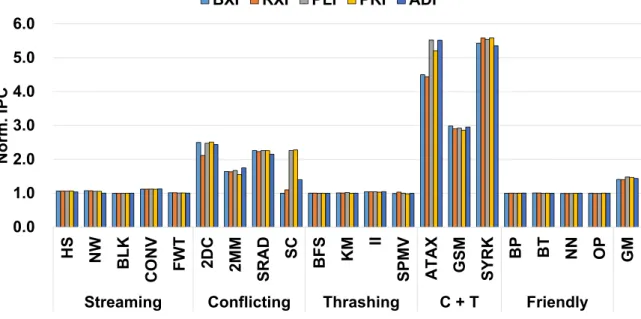
Figure 10 demonstrates that the ACI schemes significantly improve the performance of some benchmarks, especially the conflicting and conflicting and thrashing (C+T) benchmarks. Specif-ically, BXI, RXI, PLI, PRI, and ADI provide corresponding performance improvement of 40.2%, 39.8%, 47.0%, 45.8%, and 42.3% over the conventional indexing scheme on average (i.e., geo-metric mean). In addition, the ACI schemes incur little or no performance degradation across all of the evaluated benchmarks.
0.0 1.0 2.0 3.0 4.0 5.0 6.0 HS NW BLK CONV FWT 2DC 2MM SRAD SC BFS KM II SPMV ATAX GSM SYRK BP BT NN OP GM Streaming Conflicting Thrashing C + T Friendly
Norm. IPC
BXI RXI PLI PRI ADI
Figure 10: Overall performance results of the ACI schemes applied to the L1 data cache
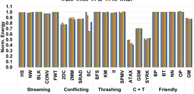
Figure 11 shows that the ACI schemes significantly reduce the energy consumption, especially the conflicting and conflicting and thrashing (C+T) benchmarks. Specifically, BXI, RXI, PLI, PRI, and ADI provide corresponding energy reductions of 10.7%, 11.0%, 13.2%, 12.7%, and, 12.1% over the conventional indexing scheme on average (i.e., geometric mean). Similarly to the performance result trend, the ACI schemes incur little or no increase in their energy consumption levels across all the evaluated benchmarks.
To gain deeper insight into the performance and energy results, we provide detailed cycle and energy breakdowns of a subset of the evaluated benchmarks. To maintain variety yet conciseness, we investigate the seven benchmarks among all the evaluated benchmarks by selecting at least one benchmark from each category which exhibits different performance and energy trends when the ACI schemes are applied.
Figure 12 shows the execution cycle breakdown of the seven benchmarks. For each bench-mark, we run it with 6 different indexing configurations for the L1 data cache. Each bar is normalized to the baseline version in which the conventional indexing scheme is used for the L1 data and L2 caches. Each bar consists of multiple segments, each indicating busy cycles, idle cycles due to a load imbalance across SIMT cores (Idle Core), idle cycles spent when no warp is ready to execute (Idle Warp), cycles spent for ALU (PL ALU), LDST (PL LDST), and both (PL Both) pipeline stalls, and cycles stalled at the scoreboard, waiting for the data produced by ALU (SB ALU), LDST (SB LDST), and both (SB Both) instructions.
Figure 12 shows that the ACI schemes significantly improve2DC,ATAX, andSYRKperformance outcomes. For these benchmarks, the ACI schemes effectively reduce L1 data cache misses (Fig-ure 13(a)) and reservation fails (Fig(Fig-ure 13(b)), which eventually reduces the LDST stall cycles (i.e., the “PL LDST" segment in Figure 12). In particular, regardingATAX, ADI outperforms all
0.0 0.1 0.2 0.3 0.4 0.5 0.6 0.7 0.8 0.9 1.0 1.1 HS NW BLK CONV FWT 2DC 2MM SRAD SC BFS KM II SPMV ATAX GSM SYRK BP BT NN OP GM Streaming Conflicting Thrashing C + T Friendly
Norm.
Energy
BXI RXI PLI PRI ADI
Figure 11: Overall energy results of the ACI schemes applied to the L1 data cache
static cache indexing schemes by successfully identifying and utilizing the important bits as the indexing bits based on the runtime information (Section 3.1).
Some of the ACI schemes show different performance trends than the others. For NW, ADI is ineffective compared to the other schemes. This is mainly due to the short kernel execution time of NW, eventually providing insufficient adaptation opportunities for ADI.
For SC, BXI, RXI, and ADI are outperformed by PLI and PRI. Some of the high bits in the memory address are effective for reducing the cache contention of SC. However, BXI, RXI, and ADI are designed mostly to utilize the lower bits for constructing the indexing bits to provide higher performance across a wide range of applications (BXI and RXI) and maintain low hardware complexity (ADI) [32]. Therefore, BXI, RXI, and ADI show suboptimal performance for SC. In contrast, PLI and PRI achieve higher performance by effectively utilizing the most significant bits.
For 2DC, RXI is significantly outperformed by BXI. This occurs mainly because some of the higher bits employed by RXI to construct the indexing bits are less effective for mitigating the intra-warp interference incurred in 2DC. Figures 13(a) and 13(b) also show that RXI incurs significantly more L1 data cache misses and reservation fails than BXI.
Finally, the performance impact of the ACI schemes is negligible for BFS and BT. This is mainly because they are highly hand optimized schemes to facilitate the coalescing of the memory addresses requested by the threads in the same warp, limiting the effect of the ACI schemes. For these benchmarks, Figure 13 shows that the L1 data cache misses and reservation fails remain rather unaffected when the ACI schemes are applied to the L1 data cache.
We now investigate the energy efficiency of the ACI schemes. Figure 14 shows the energy consumption normalized to the conventional indexing scheme. The L1 data cache, NOC, L2,
0.0 0.1 0.2 0.3 0.4 0.5 0.6 0.7 0.8 0.9 1.0 1.1
CVI BXI RXI PLI PRI ADI CVI BXI RXI PLI PRI ADI CVI BXI RXI PLI PRI ADI CVI BXI RXI PLI PRI ADI CVI BXI RXI PLI PRI ADI CVI BXI RXI PLI PRI ADI CVI BXI RXI PLI PRI ADI
NW 2DC SC BFS ATAX SYRK BT
Norm. Cycles
Busy Idle Core Idle Warp PL ALU PL LDST
PL Both SB ALU SB LDST SB Both
Figure 12: Execution cycle breakdown of the conventional and ACI schemes applied to the L1 data cache 0.0 0.2 0.4 0.6 0.8 1.0 1.2 NW 2DC SC BFS ATAX SYRK BT Norm. L1 Misses
BXI RXI PLI PRI ADI
(a) Misses 0.0 0.2 0.4 0.6 0.8 1.0 1.2 NW 2DC SC BFS ATAX SYRK BT Norm. L1 RFs
BXI RXI PLI PRI ADI
(b) Reservation fails
Figure 13: L1 data cache misses and reservation fails of the conventional and ACI schemes applied to the L1 data cache
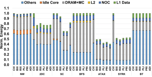
DRAM+MC, idle core, and others (mainly related to SIMT cores) segments indicate the energy consumed by the corresponding hardware components. Figure 14 shows that the ACI schemes significantly improve the energy efficiency for a subset of the evaluated benchmarks (i.e., 2DC, SC, ATAX, and SYRK), demonstrating the potential of ACI schemes to realize high performance and energy efficient GPGPU computing. For these benchmarks, we observe that the energy reduction is mainly achieved from the reduction in the non-memory hardware components (i.e., the idle core and others). Similar to the performance results, the energy consumption of BFS and BTremains unaffected with the ACI schemes.
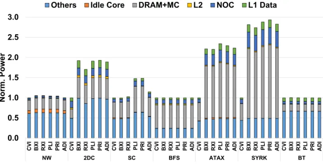
To gain a deeper understanding of the energy reduction realized with ACI schemes, Figure 15 shows the power consumption normalized to the conventional indexing scheme. For the bench-marks that result in an energy reduction with the ACI schemes, we observe that power consumed
0.0 0.1 0.2 0.3 0.4 0.5 0.6 0.7 0.8 0.9 1.0 1.1
CVI BXI RXI PLI PRI ADI CVI BXI RXI PLI PRI ADI CVI BXI RXI PLI PRI ADI CVI BXI RXI PLI PRI ADI CVI BXI RXI PLI PRI ADI CVI BXI RXI PLI PRI ADI CVI BXI RXI PLI PRI ADI
NW 2DC SC BFS ATAX SYRK BT
Norm.
Energy
Others Idle Core DRAM+MC L2 NOC L1 Data
Figure 14: Energy consumption breakdown of the conventional and ACI schemes applied to the L1 data cache
by the hardware components (e.g., DRAM and memory controllers) in the memory hierarchy increases. Note that, with the ACI schemes, reservation fails in the L1 data caches are signifi-cantly reduced. This allows for more memory requests per unit time to be performed through the hardware components in the memory hierarchy, increasing their dynamic power consump-tion. However, because the overall memory traffic is reduced with fewer L1 data cache misses (Figure 13(a)), ACI marginally reduces the energy consumption of the hardware components in the memory hierarchy.
Figure 15 shows that the power consumption of the non-memory hierarchy components (i.e., idle cores and others) is less significantly affected than the hardware components in the memory hierarchy with the ACI schemes. This occurs because the non-memory hierarchy components continues to consume dynamic power even for instructions that have been issued but have failed to execute due to events such as reservation fails. In addition, the “others” segment includes the static power consumption, which is not affected by the use of the ACI schemes. As such, combined with the reduced execution cycles, the energy reduction stemming from the non-memory hierarchy components accounts for a significant portion of the total energy reduction for the aforementioned benchmarks with the ACI schemes.
3.4.3 Effectiveness of Advanced Cache Indexing for the L2 Cache
This section investigates the effectiveness of ACI for the L2 cache.4 For each benchmark, we run it with 8 different cache indexing configurations. Each configuration is labeled with two
4
Because the RXI scheme has been reverse-engineered only for the L1 data cache but not for the L2 cache [29], we are unable to investigate the effectiveness of RXI with regards to the L2 cache.
0.0 0.5 1.0 1.5 2.0 2.5 3.0
CVI BXI RXI PLI PRI ADI CVI BXI RXI PLI PRI ADI CVI BXI RXI PLI PRI ADI CVI BXI RXI PLI PRI ADI CVI BXI RXI PLI PRI ADI CVI BXI RXI PLI PRI ADI CVI BXI RXI PLI PRI ADI
NW 2DC SC BFS ATAX SYRK BT
Norm.
Power
Others Idle Core DRAM+MC L2 NOC L1 Data
Figure 15: Power consumption breakdown of the conventional and ACI schemes applied to the L1 data cache
letters. The first and second letters denote the cache indexing scheme used for the L1 data and L2 caches, respectively. Each letter indicates one of the following cache indexing schemes – conventional (C), bitwise XOR (B), polynomial modulus (L), prime modulo (R), and adaptive (A) indexing schemes. For example, the LL configuration indicates that PLI is used for the L1 data and L2 caches. For another example, the AC configuration indicates that the adaptive and conventional indexing schemes are used for the L1 data and L2 caches, respectively. Using these configurations, we quantify the additional performance and energy efficiency gains of the ACI schemes applied to the L2 cache.
For all 20 evaluated benchmarks listed in Table 7, BXI, PLI, PRI, and ADI improve the performance by 57.1%, 69.9%, 65.7%, and 59.8% and reduce the energy consumption by 28.0%, 32.3%, 29.3%, and 27.9%, respectively, over the conventional indexing scheme. To keep the discussion concise and focused, we discuss the experimental results of the four benchmarks (i.e., 2DC,SC,BFS, andATAX), each of which exhibits different performance and energy efficiency trends with the ACI schemes applied to the L2 cache.
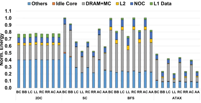
Figure 16 shows the execution cycle breakdown normalized to the results of the conventional indexing scheme applied to the L1 data and L2 caches. To quantify the additional performance gain of the ACI schemes applied to the L2 cache, we report the results with the schemes only applied to the L1 data cache and both the L1 data and L2 caches. For 2DC, the ACI schemes applied to the L2 cache have an insignificant performance effect because the memory controller and DRAM form the major performance bottleneck due to bandwidth saturation.
In contrast, the ACI schemes provide a significant additional performance gain for SC,BFS, and ATAX when they are applied to both the L1 data and L2 caches, mainly because these
0.0 0.1 0.2 0.3 0.4 0.5 0.6 0.7 0.8 0.9 1.0 1.1 BC BB LC LL RC RR AC AA BC BB LC LL RC RR AC AA BC BB LC LL RC RR AC AA BC BB LC LL RC RR AC AA 2DC SC BFS ATAX Norm. Cycles
Busy Idle Core Idle Warp PL ALU PL LDST
PL Both SB ALU SB LDST SB Both
Figure 16: Execution cycle breakdown of the conventional and ACI schemes applied to the L1 data and L2 caches
0.0 0.2 0.4 0.6 0.8 1.0 2DC SC BFS ATAX Norm. L2 Misses
BXI PLI PRI ADI
(a) Misses 0 1 2 3 4 5 6 2DC SC BFS ATAX Norm. L2 RFs
BXI PLI PRI ADI
(b) Reservation fails
Figure 17: L2 data cache misses and reservation fails of the conventional and ACI schemes applied to the L1 data and L2 caches
schemes effectively reduce the number of L2 reservation fails (Figure 17(b)), eventually leading to a reduction in the LDST pipeline (i.e., the PL LDST segment in Figure 16) and fewer scoreboard stalled (i.e., the SB LDST segment) cycles.5
BXI and ADI provide smaller performance gains for SC than for the other ACI schemes because they do not employ most significant bits, which are highly effective for mitigating the cache contention issue, for indexing6 For instance, Figure 17(a) shows that BXI incurs 5For 2DC, the number of reservation fails in the L2 cache greatly increase with the ACI schemes because
significantly more memory requests per cycle are sent to the L2 cache due to the reduced reservation fails in the L1 data cache enhanced with the ACI schemes.
6
As in case of the L1 data cache, BXI and ADI applied to the L2 cache are designed to utilize the lower bits of a memory address when constructing the indexing bits to achieve higher performance across a wide range of applications (BXI) and to maintain low hardware complexity (ADI).
0.0 0.1 0.2 0.3 0.4 0.5 0.6 0.7 0.8 0.9 1.0 1.1 BC BB LC LL RC RR AC AA BC BB LC LL RC RR AC AA BC BB LC LL RC RR AC AA BC BB LC LL RC RR AC AA 2DC SC BFS ATAX Norm. Energy
Others Idle Core DRAM+MC L2 NOC L1 Data
Figure 18: Energy consumption breakdown of the conventional and ACI schemes applied to the L1 data and L2 caches
significantly more L2 cache misses than the other ACI schemes. In addition, it is interesting that while the ACI schemes have insignificant performance effects on the L1 cache for BFS, they significantly improve the performance when they are applied to the L2 cache. This clearly demonstrates the importance of holistically optimizing the hardware caches in the GPGPU memory hierarchy.
We now investigate the energy efficiency of the ACI schemes applied to the L2 cache. Fig-ure 18 shows the energy consumption breakdown normalized to the results of the conventional indexing scheme applied to the L1 data and L2 caches. For2DC, the ACI schemes have insignifi-cant effects on energy consumption because the major performance bottlenecks are the memory controller and DRAM.
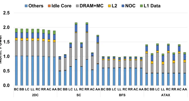
In contrast, the ACI schemes significantly reduce the energy consumption of SC, BFS, and ATAXwhen they are applied to both the L1 data and L2 caches. In a closer analysis of the energy consumption results, Figure 19 shows the power consumption breakdown normalized to the re-sults of the conventional indexing scheme applied to the L1 data and L2 caches. The ACI schemes applied to the L2 cache increase the power consumption of SC significantly, mainly due to the increased power consumption of the memory hierarchy components (e.g., NOC, DRAM+MC) because more memory requests per cycle can be transmitted through the memory hierarchy by effectively mitigating the L2 cache contention issue using the ACI schemes. However, the perfor-mance improvement of the ACI schemes effectively cancels out the increased power consumption, significantly reducing the energy consumption ofSC.
Interestingly, the ACI schemes applied to the L2 cache reduce both the energy and power consumption outcomes forBFSandATAX. The ACI schemes significantly reduce L2 cache misses
0.0 0.5 1.0 1.5 2.0 2.5 BC BB LC LL RC RR AC AA BC BB LC LL RC RR AC AA BC BB LC LL RC RR AC AA BC BB LC LL RC RR AC AA 2DC SC BFS ATAX Norm. Power
Others Idle Core DRAM+MC L2 NOC L1 Data
Figure 19: Power consumption breakdown of the conventional and ACI schemes applied to the L1 data and L2 caches
with these benchmarks as well. In other words, the L2 cache effectively filter out the memory requests that would be sent to the memory controller and DRAM when using the conventional indexing scheme, reducing the power consumption by these components. Combined with the reduced power consumption and fewer execution cycles, the ACI schemes significantly reduce the overall energy consumption ofBFS and ATAX.
3.4.4 Sensitivity of Advanced Cache Indexing to Architectural Parameters
This section investigates the performance sensitivity of the ACI schemes to key architectural parameters, in this case the indexing latency, cache associativity, and capacity. To compile the performance sensitivity results, we apply the advanced indexing schemes to the L1 data cache and the conventional indexing scheme to the L2 cache.
Given the rather complicated hardware logic of some of the ACI schemes (e.g., PLI) located along the critical path, they can introduce additional indexing latency [30], especially as the SIMT core frequency aggressively scales in the future generation of GPGPU architectures. To quantify the performance effect of the additional indexing latency, we compare the performance of PLI by sweeping the additional indexing latency from 0 to 4. We investigate the performance sensitivity of PLI to indexing latency because (1) the hardware logic of PLIthat computes the indexing bits is in the critical path, and (2) this scheme shows high performance and energy efficiency across a variety of the evaluated benchmarks.
On average, the performance impact of the additional latency is rather insignificant. Specif-ically, the average performance degradation rates across all the 20 benchmarks listed in Table 7 are 0.9%, 1.3%, 2.8%, and 5.7% when the additional indexing latency is set to 1, 2, 3, and 4