1010.1
Structures
Matjaž KoželjJožef Stefan Institute Jamova 39
SI-1000, Ljubljana, Slovenia [email protected]
Bruno Cvikl
Faculty of Energy Technology and Faculty of Civil Engineering, University of Maribor Hočevarjev trg 1
SI-8270, Krško, Slovenia [email protected]
ABSTRACT
Uses of organic semiconductors have expanded in last two decades. In spite of some inherent problems regarding the use for the detection of ionising radiation, considerable number of detectors has been proposed. In this paper, we briefly describe differences between organic and inorganic semiconductors and summarise published work in the field of detection of ionising radiation with organic semiconductors.
Detection of neutrons requires some specific methods, which usually include conversion of neutrons to some other form of ionising radiation. The application of the approach for the detection of neutrons with inorganic semiconductor detectors is already established, while the use for organic semiconductor detectors is just at the beginning.
Based on our previous work with organic semiconductors, we propose neutron detector based on organic heterojunction structure and boron converter. It seems that the detector is feasible, and should be usable down to neutron fluxes 106cm-2s-1.
1 INTRODUCTION
One of the promising fields of implementation of organic semiconductors is field of sensors and detectors. Due to the variety of chemical and physical properties, organic semiconductors could serve as a starting material for technologies that will produce not just new, but also improved and cheaper sensors and detectors. Extensive work in this field has been done already, especially with different polymers that can be successfully tailored for the use as sensors for particular gases, chemical and biological substances (biosensors) [1].
Materials that are regularly used for different types of detectors are inorganic semiconductors. The fast development in semiconductor technology in the last decades was extremely beneficial for the progress in technology of inorganic semiconductor detectors, enabling improvement of existing detectors, and development of new types. Detectors for ionising radiation have also benefited from that progress. The earliest detectors for ionising radiation based on inorganic semiconductor (germanium) were developed at the end of the fifties and later became the most desired tool for measurements and research in different fields of science where ionising radiation is present. Today, detectors for ionising radiation
based on inorganic semiconductors are standard tool for scientists and engineers dealing with sources of ionising radiation. The fast response and general ruggedness of inorganic semiconductor detectors makes them also attractive for variety of neutron detection applications (see e.g. [2]).
Regarding the use of organic semiconductors for detection and measurement of ionising radiation some problems were anticipated in advance. Evidences on effects of ionising radiation to organic semiconductors, like radiation damage [3] and low charge carrier mobility, were reasons that predicted properties of possible devices built on organic semiconductors were inferior to existing sensors based on inorganic semiconductors. Nevertheless, some attempts to evaluate possibility to use organic semiconductors have been done in the recent years, but much is still to be done.
2 ORGANIC SEMICONDUCTORS
2.1 Organic semiconductors vs. inorganic semiconductors
Inorganic semiconductors consist of single element atoms (Ge, Si) or two elements at most (e.g. in GaAs), which are arranged in crystal lattice and connected with (strong) covalent bonds. Overlapping of bond electron wave functions from many atoms produces energy bands where electrons (and holes) are not localised (tied to a certain atom), but can move through the lattice. In fact, this mobility requires free energy levels, which are available in the highest (conduction) band. To reach the conduction band, electron must “overcome” band gap (Ge: 0.66 eV, Si: 1.12 eV, GaAs: 1.42 eV), i.e. energy gap between valence and conduction band, which requires some additional energy. For certain (but small) part of electrons in crystal, this energy is provided from thermal movement of crystal lattice. Addition of dopants increases the number of “free” electrons in conduction band (or “free” holes in valence band) for more orders of magnitude and alters conduction properties of semiconducting crystal. Today’s technology is capable of high precision tailoring of material properties and of creation of complex microscopic structures utilising this approach.
On other side, organic semiconductors consist of smaller or larger organic molecules with π-bonds between carbon atoms. Due to similar energy to σ-bonds between carbon atoms, π-bonds can travel from one pair of carbon atoms to neighbouring pair. In fact, it happens so fast and so often, that chemists speak about delocalised bonds that enable travelling of electron (charge) over a chain of carbon atoms. Namely, π-bonds of chained carbon atoms create two energy bands with 2.5 ~ 3.0 eV gaps, where the higher band consists of mostly free (available) energy states, similarly to conduction band in inorganic semiconductors, and lower energy band that is mostly populated. The creation of these bands, usually named LUMO (Lowest Unoccupied Molecular Orbit) and HOMO (Highest Occupied Molecular Orbit) for benzene ring is presented on Figure 1. Due to the similarity to description of electron energy levels in inorganic semiconductors, these bands are also sometimes named as conduction and valence band.
Molecules with delocalised π-bonds can have different number of carbon atoms. For convenience, organic semiconductors are usually subdivided into three categories, small molecules, oligomers and polymers, depending on the length of molecular structure that sets mechanical, chemical and electronic properties. While the charge transport in particular molecule is due to the delocalised π-bonds, charge transfer from one molecule to other molecule is much more accidental. Neighbouring molecules are connected with weaker Van der Waals forces and transfer of charge can happen in different ways: it can be through tunnelling, or through localised states, or phonon-assisted hopping. All these mechanisms are
strongly dependent on arrangement of molecules, inclusions and physical conditions (e.g. stress). Electrical properties of organic semiconductors are therefore heavily influenced by the conditions of processing. Typically, small molecules are deposited in vacuum chambers where even crystalline films could be achieved, while oligomers and polymers are deposited from liquid solutions and self-arrangement of these molecules could be enhanced with either proper tailoring of molecular structure (e.g. adding of side chains) or some other approaches.
a) b)
Figure 1: a) Benzene ring with system of delocalised π-bonds. b) Scheme of energy levels of σ- and π-bonds, creating valence (HOMO) and conduction band (LUMO) [4].
Similarly to inorganic semiconductors, electrical properties of organic semiconductors could be changed with addition of other materials (see e.g. [5]). In this case, dopants are usually molecules mixed with organic semiconductor material during processing. For bipolar structures, it is necessary to use molecules of sufficient size (larger aromatic molecules that are strong π-electron donors or acceptors are used), since atoms and small molecules (in comparison to organic semiconductor molecules) easily diffuse through semiconductor material and structures are not thermally stable. In fact, practically all gases diffuse into organic semiconductors, which should be taken into account during processing and evaluation of semiconductor properties. Due to these problems, doping of organic semiconductors is not used as regular technological approach as it is for inorganic semiconductors, but is limited to certain applications.
Understanding of organic semiconductors is far from current understanding of inorganic semiconductors, and so is the possibility to predict properties of combination of these materials in different structures reliably. For description of electrical properties and behaviour of bulk materials and structures, analogies with the inorganic semiconductors are used, but this approach is not always successful: established models should be verified experimentally and modifications introduced (see e.g. [6]).
2.2 Detection of ionising radiation with organic semiconductors
The first attempts to evaluate the influence of ionising radiation to organic semiconductors were performed in late nineties. Early reports concentrated on measurement of some material properties, like charge transport in polymer polyacetilene, PPV (polyphenilen-vinylene), poly(3-phenylene)-acetilene and polyvinylkarbazol foils under radiation [7], and change of optical properties and related shift of HOMO and LUMO bands, change in conduction and capacitance under the influence of γ radiation in Ag/MnPC/Ag structure [8]. In the first case the authors were able to confirm and analyse the transport of charges released due to irradiation in polyacetilene and PPV foils, but were not able detect observable changes in other two materials mentioned. In second case, the authors used extremely high γ-ray doses (~10kGy) and were able to confirm the change in optical properties, increase of bulk conductivity and decrease of capacitance with increasing dose to Ag/MnPC/Ag structure.
Low efficiency of detection for γ-rays (and X-rays, also) is not only the consequence of low atomic numbers of organic semiconductor constituents. Problems are also low mobility of charges (it is the consequence of charge transport mechanism) and excitons, localised excited states that occur in organic molecules after energy absorption. Namely, after energy absorption negatively charged electron in LUMO band cannot “separate” from positively charged hole in HOMO band; they are bounded inside molecule with binding energy which is larger (typically 0.1 to 0.4 eV) than the thermal energy [9]. Exciton disintegration could be enhanced with application of external electric field, or even more effectively with mixing (blending) different semiconductors. Acceptable results for certain semiconductors could be achieved just by creating junction with other semiconductor. This approach is typically used for organic optical photo diodes (OPD), which were also tested as a detector for X-rays [10]. While achieved sensitivity (in the range of therapeutic dose rates) was sufficient, linearity of response was not satisfactory.
Alternate approach to detection of X and γ rays is combination with classical scintillation materials. The idea is to substitute actual light detector (photomultiplier or silicon photodiode) with coating of organic semiconductor [11]. This semiconductor coating could be pixellated enabling the spatial reconstruction of scintillation signal.
3 DETECTION OF NEUTRONS
3.1 Background of neutron detection
Since neutrons are indirectly ionising radiation, detection of neutrons always involves some conversion or energy transfer either to charged particles or to γ radiation. For fast neutrons, the mechanism of conversion is elastic neutron scattering on light nucleus (e.g. 1H or 12C nuclei in H2, CH4 proportional detectors or plastic scintillators, or 4He nuclei in He
proportional detector). Beside scattering, also (n, p) reaction on 3He and (n, ) reaction on 6Li are used for detection and spectroscopy of fast neutrons in gas and scintillation counters [12].
Very useful are also different threshold nuclear reactions that require neutrons with some minimum energy in order to take place at all. These reactions could be used for activation detectors (foils or wires) which are evaluated (i.e. activity is measured) after exposure to neutrons (see e.g. [12]).
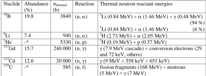
Detection of thermal neutrons relies exclusively on nuclear reactions. Table 1 presents the most important data for reactions, which are used for thermal neutrons detection. Material with neutron sensitive nuclides is either incorporated or located in direct contact with detector capable of identifying thermal neutron reactants.
One of the problems of neutron detection is that neutron radiation is always mixed with γ radiation and detector should enable identification (and discrimination) of signals from γ radiation. This could be relatively simple done for gas detectors (with BF3 or 3He) where
interaction probability for neutrons is approximately 500 (BF3) to 7700 (3He) times higher
than probability for γ-rays and ratio of neutron to electron (from γ interaction) energy deposition about 100 [13].
For fast neutrons, problems with γ-rays elimination are even greater. Ratio of interaction probability in gas detectors (e.g. 4He) is just 10 times higher for neutrons then for γ-rays and only 3 times higher for scintillator detector, while energy deposited from neutron is just 20 times higher than energy deposited from electron (from γ interaction) and only 2.5 times higher in scintillator detector. Signals from γ-rays and neutrons therefore overlap and additional efforts are required to distinguish them [13].
Table 1: Important data for thermal neutrons sensitive nuclides Nuclide Abundance
(%)
σthermal
(b)
Reaction Thermal neutron reactant energies
10
B 19.8 3840 (n, ) 7Li (0.84 MeV) + (1.46 MeV) + γ (0.48 MeV)
(94 %) 7 Li (0.84 MeV) + (1.46 MeV) (6 %) 6 Li 7.4 940 (n, ) 3H (2.73 MeV) + (2.05 MeV) 3 He -* 5330 (n, p) 3H (0.19 MeV) + p (0.57 MeV) 157
Gd 15.7 240 000 (n, γ) γ (7.9 MeV cascade) + conversion electrons (29
and 72 keV, others)
113
Cd 12.6 20 000 (n, γ) γ (9 MeV + 558 keV + 651 keV)
235
U -* 585 (n, f) fission fragments (168 MeV) + neutrons
(5 MeV) + γ (7 MeV) *not used as natural mixture of isotopes
3.2 Neutron detection with inorganic semiconductors
Inorganic semiconductor detectors for fast neutrons use threshold reactions as conversion mechanism [14]. For example, (n, ) reaction on 12C has threshold 6.2 MeV and energy release 2.2 MeV. Similarly, (n, ) and (n, p) reactions on 28Si have thresholds of roughly 7 MeV. Diamond and silicon solid-state detectors, which use these reactions, could be manufactured as a bulk and as thin film devices.
For thermal neutrons, one approach is to use bulk semiconductor containing the neutron converter nuclide. The most studied is B5C, but the production is very demanding. Other
candidates are polycrystalline BN and polycrystalline LiF, which could be embedded in inorganic or organic binder [15].
Other, more straightforward approach is to merge silicon diode detector with converter layer. Silicon diode detectors are used for charged particle and radiation detection and spectroscopy, which, in principle, enable detection of reactants from thermal neutron reactions on converter. But since silicon diode detector is also sensitive to γ radiation it seems, that the best converter for thermal neutrons is 157Gd, due to the high microscopic cross-section and possibility to use thicker layer of material [16]. For 10B or 6Li the thickness of usable converter layer is limited with the range of particles, which is approximately three μm. This limits the usability to applications where low efficiencies are required.
4 ON THE POSSIBLE USE OF ORGANIC SEMICONDUCTORS FOR
NEUTRON DETECTION
If we consider possibilities of neutron detection with organic semiconductors, then we have similar choices like with inorganic semiconductors. We can use either bulk material or approach similar to silicon diode detectors we have just described. Since the technology of crystal growth of organic semiconductor is not available to us, we will concentrate on second approach. We will also limit to detection of thermal neutrons, due to the importance for nuclear reactor operation. Our proposed detector should have converter layer covering the detector for charged particles.
In the past [17] we have made some preliminary measurements with radiation on organic bilayer structure which consisted of 0.8 μm PTCDA (3,4,9,10-perylenetetracarboxylic dianhydride) and 1.25 μm CuPC (copper phthalocyanine) layers on ITO (indium tin oxide)
covered glass base. Other contact was 0.75 μm aluminium layer deposited on the upper (PTCDA) layer. The diameter of aluminium contact, which defined active area, was 1.5 mm. Organic semiconductors were deposited in our laboratory with Ionised Cluster Beam (ICB) method, while aluminium was deposited with simple evaporation. For measurements 90 kBq
241
Am source was used. 241Am is source of 5.486 and 5.443 MeV particles and 59.5 keV γ rays, which did not interfere with our measurements. Under irradiation, I-V and C-V measurements on our sample have shown increase of reverse current for ~10-11 A and increase of capacitance from 39 to 41 pF. We were surprised with the results, since they were implicating (unrealistically) high ionisation yield. Evaluation of results have shown that mean energy for production of electron-hole pair was 0.4 eV which is less than 20 % of band gap in these organic semiconductors. Since the sample was previously exposed to air, inclusion of oxygen could be the reason for observed anomaly. Reason could be also high density of traps in semiconductor bulk. However, we were able to confirm these results in subsequent measurements; therefore, we believe that we have proved ability of our bilayer structure to detect radiation.
If we want to use similar structure for the detection of neutrons, then it should include a converter layer. If we put converter layer on top of our structure, than the Al layer will serve as contact layer and also as boundary between organic semiconductor and converter layer. Scheme of suggested structure is on Figure 2.
ITO (contact) CuPc PTCDA Aluminium (contact) Glass Converter
Figure 2: Scheme of proposed structure for neutron detection
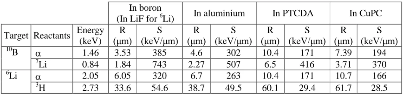
Possible candidates for converter layer are boron (or some boron compound) or lithium containing compounds (like LiF). In Table 2, we have listed range R and stopping power S for reactants in boron, lithium fluoride (LiF), aluminium and our organic semiconductors PTCDA and CuPC.
Table 2: Range R and stopping power S in converter, Al, PTCDA and CuPC. Data were computed with SRIM program [18]
In boron
(In LiF for 6Li) In aluminium In PTCDA In CuPC
Target Reactants Energy
(keV) R
(μm) (keV/μm) S (μm) R (keV/μm) S (μm) R (keV/μm) S (μm) R (keV/μm) S
10 B 1.46 3.53 385 4.6 302 10.4 171 7.39 194 7 Li 0.84 1.84 743 2.27 507 6.5 416 3.71 370 6 Li 2.05 6.05 320 6.7 263 10.4 171 10.7 166 3 H 2.73 33.6 54.6 38.7 49.5 60.1 29.4 61.7 28.5
Since thickness of our organic layers is approximately one μm, we can see that boron has advantage over lithium due to higher stopping power (and consequently higher energy transfer) to organic layers. 6Li has smaller cross section, but higher energies of reactants, which is not advantageous in our case. Self-absorption limits the usable thickness of converter (for boron approximately to 1 to 2 μm (since ions must also penetrate aluminium layer and still have enough energy for ionisation in organic layers).
If we decide for 1 μm converter layer from natural boron (19.9% of 10
B) and put the structure in neutron flux 1×10¹⁰
cm-2 s-1, reaction rate in converter will be approximately 108 cm-2s-1 with half of particles and 7Li ions travelling to the aluminium and organic layers. Considering data from Table 2, we can estimate energy deposited in organic layers. This energy (8×10¹³
eV cm-2 s-1) is converted to free holes and electrons in organic semiconductor layers. As a replacement for of our previous (unconfirmed) estimate for electron-hole production energy, we prefer to use an estimate used for inorganic semiconductors, i.e. that electron-hole production energy is approximately three times energy of energy gap, although some reported results for organic semiconductors [7] are even ten times larger. Using this estimate, we get 1×10¹¹
electron-hole pairs per second per each cm2 of bilayer, or, if we express it as generated current, 3.5×10⁻⁶ A/cm2, which should be easily detectable. For comparison, our “old” structure (smaller surface) with added converter would generate 7×10⁻⁸
A in the flux 1×1010 cm-2 s-1.
The lowest detectable neutron flux depends on our ability to accurately measure low currents, but measurement of currents down to 10-10 A (i.e. flux 3×106 cm-2 s-1) should not be problem.
During this discussion, we have not mentioned the γ radiation, which usually accompanies neutron radiation. Since our structure is thin, and all atoms have low atomic number, sensitivity to γ radiation should be extremely low and should not interfere with neutron measurements.
There is also a problem of activation of elements in our structure. The biggest problem is glass where 31Si (t1/2=2.62 h) would be produced. In aluminium layer short-lived 28Al
(t1/2=2.24 min) would be produced and in ITO layer smaller activities of short-lived 114In
(t1/2=72 s) and 121Sn (t1/2=27 h) would be the most important activation products. All other
activated products are less important.
5 CONCLUSIONS
Organic semiconductors are promising new material for variety of detectors. This applies also to detection of ionising radiation, where certain problems delay the introduction in regular use.
Detection of neutrons requires introduction of some converter nuclei in detectors, which presents additional problem for device construction and data evaluation. Based on our previous experience with organic heterojunctions, we have proposed a detector, which uses boron as converter, and organic heterojunction diode that detects charged reactants.
Neutron induced current for the detector that consists of a boron layer (1 μm, natural isotope composition), Al layer (0.75 μm, serves as contact and separation layer), and PTCDA/CuPC organic bilayer (2.05 μm) on ITO conductive layer, was estimated to be about 3×10⁻⁶ A/cm2 for neutron flux 1×10¹⁰ n cm-2 s-1, which should be easily detectable.
It seems that proposed detector is feasible and could be used for neutron fluxes down to 106 cm-2s-1.
REFERENCES
[1] B. Adhikari, S. Majumdar, “Polymers in sensor applications,” Progress in Polymer Science, 29, 2004, pp. 699–766.
[2] A. Peurrung, “Recent developments in neutron detection,” Nuclear Instruments and Methods in Physics Research Section A: Accelerators, Spectrometers, Detectors and Associated Equipment, 443, 2000, pp. 400–415.
[3] P. Seiler, J. D Dunitz, “Detection of Radiation Damage in Organic Crystals,” Aust. J. Phys., 38, 1985, pp. 405–412.
[4] “What are organic semiconductors.” [Online]. Available:
http://www.iapp.de/orgworld/index.php?Basics:What_are_organic_semiconductors. [Accessed: 30-Aug-2012].
[5] M. Pfeiffer, K. Leo, X. Zhou, J. . Huang, M. Hofmann, A. Werner, J. Blochwitz-Nimoth, “Doped organic semiconductors: Physics and application in light emitting diodes,” Organic Electronics, 4, 2003, pp. 89–103.
[6] B. Cvikl, “The drift-diffusion interpretation of the electron current within the organic semiconductor characterized by the bulk single energy trap level,” Journal of Applied Physics, 107, 2010, pp. 023710-023718.
[7] P. Beckerle, H. Ströbele, “Charged particle detection in organic semiconductors,” Nuclear Instruments and Methods in Physics Research Section A: Accelerators, Spectrometers, Detectors and Associated Equipment, vol. 449, 2000, pp. 302–310. [8] A. Arshak, S. Zleetni, K. Arshak, “γ-radiation Sensor Using Optical and Electrical
Properties of Manganese Phthalocyanine (MnPc) Thick Film,” Sensors, 2, 2002, pp. 174–184.
[9] M. Binda, D. Natali, M. Sampietro, T. Agostinelli, L. Beverina, “Organic based
photodetectors: Suitability for X- and Γ-rays sensing application,” Nuclear Instruments and Methods in Physics Research Section A: Accelerators, Spectrometers, Detectors and Associated Equipment, 624, 2010, pp. 443–448.
[10] E. Takada, A. Inoue, H. Imai, H. Okada, S. Naka, J. Kawarabayashi, “Application of a heterojunction organic photodiode to radiation measurement,” 2009 IEEE Nuclear Science Symposium Conference Record (NSS/MIC), 2009, pp. 1295 –1299. [11] D. Natali, M. Sampietro, “Detectors based on organic materials: status and
perspectives,” Nuclear Instruments and Methods in Physics Research Section A: Accelerators, Spectrometers, Detectors and Associated Equipment, 512, 2003, pp. 419– 426.
[12] G. F. Knoll, Radiation Detection and Measurement, 3rd ed. Wiley, 2000. [13] T. W. Crane, M. P. Baker, “Neutron Detectors.” [Online]. Available:
http://www.fas.org/sgp/othergov/doe/lanl/lib-www/la-pubs/00326408.pdf. [Accessed: 17-Jun-2012].
[14] B. D. Milbrath, A. J. Peurrung, M. Bliss, W. J. Weber, “Radiation detector materials: An overview,” Journal of Materials Research, 23, 2008, pp. 2561–2581.
[15] M. Schieber, A. Zuck, G. Marom, O. Khakhan, M. Roth, Z. B. Alfassi, “Composite polycrystalline semiconductor neutron detectors,” Nuclear Instruments and Methods in Physics Research Section A: Accelerators, Spectrometers, Detectors and Associated Equipment, 579, 2007, pp. 180–183.
[16] C. Petrillo, F. Sacchetti, O. Toker, N. . Rhodes, “Solid state neutron detectors,” Nuclear Instruments and Methods in Physics Research Section A: Accelerators, Spectrometers, Detectors and Associated Equipment, 378, 1996, pp. 541–551.
[17] M. Koželj, B. Cvikl, D. Korošak, “Application of organic semiconductors for the detection of ionizing radiations,” Proc. International Conference Nuclear Energy for New Europe 2006, Ljubljana, September 18-21, Nuclear Society of Slovenia, 2006, pp. 306.1-10.
![Figure 1: a) Benzene ring with system of delocalised π-bonds. b) Scheme of energy levels of σ- and π-bonds, creating valence (HOMO) and conduction band (LUMO) [4]](https://thumb-us.123doks.com/thumbv2/123dok_us/1833322.2765341/3.892.146.755.244.454/figure-benzene-delocalised-scheme-energy-creating-valence-conduction.webp)