Virginia Commonwealth University
VCU Scholars Compass
Electrical and Computer Engineering Publications
Dept. of Electrical and Computer Engineering
2009
Effect of large strain on dielectric and ferroelectric
properties of Ba0.5Sr0.5TiO3 thin films
Bo Xiao
Virginia Commonwealth University, xiaob@vcu.edu
Vitaliy Avrutin
Virginia Commonwealth University, vavrutin@vcu.edu
Hongrui Liu
Virginia Commonwealth University
See next page for additional authors
Follow this and additional works at:
http://scholarscompass.vcu.edu/egre_pubs
Part of the
Electrical and Computer Engineering Commons
Xiao, B., Avrutin, V., Liu, H., et al. Effect of large strain on dielectric and ferroelectric properties of Ba0.5Sr0.5TiO3 thin films. Applied Physics Letters, 95, 012907 (2009). Copyright © 2009 AIP Publishing LLC.
This Article is brought to you for free and open access by the Dept. of Electrical and Computer Engineering at VCU Scholars Compass. It has been accepted for inclusion in Electrical and Computer Engineering Publications by an authorized administrator of VCU Scholars Compass. For more information, please contactlibcompass@vcu.edu.
Downloaded from
Authors
Bo Xiao, Vitaliy Avrutin, Hongrui Liu, Emmanuel Rowe, Jacob H. Leach, Xing Gu, Ü. Özgür, Hadis Morkoç,
W. Chang, L. M.B. Alldredge, S. W. Kirchoefer, and J. M. Pond
Effect of large strain on dielectric and ferroelectric properties
of Ba
0.5Sr
0.5TiO
3thin films
Bo Xiao,1,a兲 Vitaliy Avrutin,1Hongrui Liu,1Emmanuel Rowe,1Jacob Leach,1Xing Gu,1 Ümit Özgür,1Hadis Morkoç,1W. Chang,2L. M. B. Alldredge,2S. W. Kirchoefer,2 and J. M. Pond2
1Department of Electrical and Computer Engineering, Virginia Commonwealth University, Richmond,
Virginia 23284, USA
2
Naval Research Laboratory Washington, Washington, DC 20375, USA
共Received 14 May 2009; accepted 18 May 2009; published online 8 July 2009兲
BaxSr1−xTiO3is ideally suited as a tunable medium for radio frequency passive component. In this
context we have studied the effect of biaxial strain on the dielectric and ferroelectric properties of Ba0.5Sr0.5TiO3thin films grown epitaxially on SrTiO3共001兲substrates. The lattice parameters of the films determined by high-resolution x-ray diffraction with the thickness varying from 160 to 1000 nm indicated large biaxial compressive strain which decreased from 2.54% to 1.14% with increasing film thickness. Temperature-dependent measurements of the dielectric constant in our strained Ba0.5Sr0.5TiO3 thin films revealed a significant increase in the Curie temperature as the film thickness is below 500 nm. Enhanced ferroelectric behavior was observed for highly strained films with a remanent polarization of 15 C/cm2 in the 160-nm-thick layer. However, the thick films
共ⱖ500 nm兲 exhibited weak temperature dependence of the dielectric constant without any pronounced peak corresponding to the Curie temperature, which may suggest inhomogeneous strain distribution in the thick films. ©2009 American Institute of Physics.关DOI:10.1063/1.3151961兴
Ferroelectric materials have been extensively studied and become important for a variety of applications such as nonvolatile random access memory devices, nonlinear op-tics, motion and thermal sensors, and tunable microwave de-vices. BaxSr1−xTiO3 共BST兲 as one of widely studied
ferro-electric materials is of paramount interest as medium for tunable microwave passive components.1,2 Most of studies are focused on BST thin films because of the low cost and possible integration with mature semiconductor technolo-gies, which differ drastically from the corresponding bulk material due to the presence of strain in the thin films. Strain in BST thin films is found to be a significant factor affecting the Curie temperature and dielectric properties.3,4Therefore, tailoring strain provides an alternative approach to changing the barium-to-strontium ratio. Strain has already been uti-lized in mainstream semiconductor industry to enhance de-vice performance.5This approach generally referred as strain engineering has been extended to alter certain properties of ferroelectric materials. For example, notable change in the Curie temperature and enhancement of ferroelectric proper-ties were noted in strained strontium titanate 共SrTiO3兲 共Ref. 6兲and barium titanate共BaTiO3兲 共Ref.7兲thin films. Strained films exhibited improved ferroelectric and dielectric proper-ties compared to the intrinsic properproper-ties of the unstrained bulk materials. As a perovskite material, strontium titanate, SrTiO3共STO兲has been widely used as the substrate for
ox-ide heteroepitaxy. The similar crystal structure and close thermal expansion coefficient between BST and STO make STO a convenient substrate for growing high quality BST thin films. In this study, we have investigated strain-induced structural properties and dielectric constant as a function of temperature for a series of Ba0.5Sr0.5TiO3thin films grown on SrTiO3substrates with different thickness.
BST thin films were grown epitaxially by off-axis rf magnetron sputtering using a 3-inch-diamater Ba0.5Sr0.5TiO3
stoichiometric target. Ar and O2 gases were introduced into
the growth chamber through mass flow controllers to main-tain the growth chamber pressure at 2 mTorr with an Ar-to-O2ratio of 6:1. During growth, the substrate
tempera-ture was nominally 750 ° C according to the thermocouple reading, and the rf sputtering power was set at 120 W. These growth conditions yielded a deposition rate of about 450 Å/h for the Ba0.5Sr0.5TiO3 共BST兲layers.
The crystal structure and lattice parameters of the as-deposited BST films were determined by high resolution x-ray diffraction共HRXRD兲. High structural perfection of the BST thin films has been revealed by HRXRD 2- and
-rocking curve scans. All BST thin films exhibited exclu-sively 共00l兲 reflections and narrow -rocking curves. The full width at half-maximum 共FWHM兲 of the 共001兲 rocking curves is about 2.4 arc min for the films with a thickness of 500 nm or less. For 1000-nm-thick BST films, the generation of misfit and threading dislocations caused an increase in the FWHM value of the共001兲rocking curve to 3.6 arc min. The lattice parameters of the BST thin films were calculated from the symmetric 共001兲 and asymmetric 共011兲 XRD patterns. The peak positions of HRXRD reflections from the BST films were calibrated using reflections from the STO sub-strate as reference. Figure1shows the symmetric and asym-metric HRXRD scans of 160-, 300-, and 1000-nm-thick BST films, which clearly indicate a shift of the BST peak as the thickness changes. Both共001兲and共011兲reflections from the BST thin films are shifted to lower angles as compared to 2共001兲= 22.494° and 2共011兲= 32.032° for bulk BST of the
same composition.8As the thickness increases, one notes that the BST peak positions approach the bulk values.
The out-of-plane lattice parameter c for the BST films investigated was calculated directly from the 共001兲 reflec-a兲Electronic mail: xiaob@vcu.edu.
APPLIED PHYSICS LETTERS95, 012907共2009兲
0003-6951/2009/95共1兲/012907/3/$25.00 95, 012907-1 © 2009 American Institute of Physics
This article is copyrighted as indicated in the article. Reuse of AIP content is subject to the terms at: http://scitation.aip.org/termsconditions. Downloaded to IP: 128.172.48.59 On: Tue, 07 Apr 2015 18:00:06
tions. On the other hand, the in-plane lattice parameterawas derived from a combination of the 共011兲 asymmetric and 共001兲 symmetric reflections. Figure2 shows the lattice pa-rametersa andcas well as thec/aratio as a function of the film thickness for the BST films. These XRD measurements show that the BST films on STO substrates have a tetragonal distortion with theclattice constant being larger than that of the bulk material of the same composition. The variation of the lattice parameter c with film thickness is remarkable 共from 4.1390 to 4.0552 Å兲in the range from 160 nm to 500 nm. Note that the lattice parameter c of the 1000-nm-thick film is almost the same as that for the 500-nm-thick film. On the contrary, the in-plane lattice parameter shows a relatively small change with film thickness. It is suggested that the in-plane lattice parameter a is more confined by the sub-strate. Similar tetragonal distortion has been reported for BST films grown on MgO substrates, and the observed
dis-tortion was correlated with the oxygen pressure during growth presumably due to the generation of oxygen vacancies.9–12 Oh et al.13 reported the distortion of BST grown on MgO by rf magnetron sputtering and found that the low rf power yielded BST films with less distortion. In deposition experiments by sputtering, either high oxygen pressure or low rf power can lower the growth rate dramati-cally. A low growth rate can help to relieve strain in growing film at a relatively high growth temperature. Thus, several factors may act in unison to cause such tetragonal distortion. These factors are generally believed to be the lattice mis-match, the difference in the thermal expansion coefficients, and oxygen vacancies. Most likely, the distortion in our films is associated with lattice mismatch, since the thermal mis-match is believed to be negligible and distortion decreases with increasing film thickness due to strain relaxation.
In our experiments, the strain state of BST thin films was calculated using x12=共a−a0兲/a0 andx33=共c−a0兲/a0 for
in-plane and out-of-in-plane, respectively. The freestanding cubic lattice constant a0 of the BST film is estimated from a0=关c
+ 2共c12/c11兲a兴/关1 + 2共c12/c11兲兴, where c11 andc12are the
av-eraged elastic constants of bulk BaTiO3 and SrTiO3.14 The
BST films grown on STO are under large compressive biax-ial strain which decreases with increasing thickness of the film as shown in Fig.2共b兲. Large strain remains even for the 1000 nm film, where the in-plane and out-of-plane strain values are ⫺1.26% and 1.14%, respectively.
Measurements of the ferroelectric properties and dielec-tric permittivity for BST films grown on conductive STO: Nb 0.5% substrates 共resistivity ⬃0.05 ⍀cm兲 were undertaken with a LCR meter. Use of conductive STO substrate as the bottom electrode provides a simple and accurate way to ex-amine electrical properties and extract their parameters di-rectly. Au/Cr 共50 nm/30 nm in thickness兲circular top elec-trodes were patterned on the surface of BST films by using conventional photolithography and lift-off process. The di-ameter of the top electrode is 200 m. The ferroelectric properties of the BST films were examined by polarization-electric field 共P-E兲 measurements at T= 300 K and are shown in Fig.3. As can be seen, the 160-nm-thick BST film, which has the largest strain among the films measured, dis-plays a pronounced ferroelectric hysteresis loop with a rem-anent polarization of Pr= 15 C/cm2. The hysteresis loop
FIG. 1. XRD patterns of BST thin films with the thickness ranging from 160 to 1000 nm:共a兲symmetric共001兲2-scans and共b兲asymmetric共011兲2- scans. Arrows indicate the peak positions for the bulk Ba0.5Sr0.5TiO3.
FIG. 2.共a兲Lattice parameters共canda兲andc/aratio,共b兲strain共x12,x33兲of epitaxial BST thin films as a function of the film thickness.
FIG. 3. P-Ehysteresis loops of BST thin films with various thicknesses measured at 300 K.
012907-2 Xiaoet al. Appl. Phys. Lett.95, 012907共2009兲
for the 1000-nm-thick film at 300 K is barely detected and characterized with a small remanent polarization 共Pr = 1 – 2 C/cm2兲. The results of P-Emeasurements indicate
that the strain enhances the ferroelectric properties of epitax-ial BST thin films.
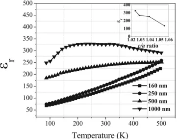
The relative dielectric constant was measured as a func-tion of temperature for a variety of BST films with thick-nesses ranging from 160 to 1 m. Figure4shows the tem-perature dependence of the out-of-plane dielectric constants
r of 160-, 250-, 500-, and 1000-nm-thick BST films mea-sured at 1 MHz. To reiterate, the lattice parameters are very sensitive to the thickness due to strain relaxation of the thin films. The thinner films 共160 and 250 nm兲, with relatively large tetragonal distortion, show temperature dependences of
rvery dissimilar to those measured for 500- and 1000-nm-thick films. As illustrated in Fig. 4, the values of the dielec-tric constant in the films with thicknesses of 160 and 250 nm increase steadily with the temperature up to 500 K共the upper limit of our measurement system兲 indicating no sign of any phase transition. The results imply that Tc of these strained BST films is much higher than that of bulk Ba0.5Sr0.5TiO3
共Tc= 250 K兲. Theory has been proposed to estimate the TC values of BST thin films under strain.3For 160- and 250-nm-thick BST film with large out-of-plane strainx33= 2.54%and
2.09%, respectively 关see Fig. 2共b兲兴, the predicted Tc in the out-of-plane direction would be around 1300–1500 K, which is far above our measurement temperatures. However, the 500- and 1000-nm-thick films exhibit very weak temperature dependences of the dielectric constant. This weak tempera-ture dependence of the dielectric constant has been attributed to inhomogeneous strain.15 Considering the large strain re-maining in the films, the influence of inhomogeneous strain might be more significant in thick strained films.
The values of dielectric constant in our single crystalline thin films are much lower than that in bulk Ba0.5Sr0.5TiO3
and polycrystalline Ba0.5Sr0.5TiO3thin films.16Small dielec-tric constant of the BST films agrees well with the theoretical analysis17 showing that the dielectric constant r decreases under large in-plane compressive strain. As seen from Fig.2, the thicker the BST thin film is, the smaller the c/a ratio becomes. It indicates that increasing film thickness induces the formation of misfit dislocations which facilitate film re-laxation. In addition, the inset in Fig.4exhibits the dielectric constant at room temperature as a function of thec/aratio, which clearly indicates the trend that the dielectric constant
r decreases with increasing strain under in-plane compres-sive strain.
In summary, we have studied strained BST thin films grown on STO substrates by rf magnetron sputtering. The structural properties measured by HRXRD reveal large in-plane compressive strain. The dielectric properties of strained BST films were examined as a function of tempera-ture. The results indicate that strain can significantly change the dielectric properties and lead a large change in the Curie temperature. Large in-plane compressive strain decreases the out-of-plane dielectric constant in BST thin films but en-hances their ferroelectric properties.
This work is supported by a grant from the Office of Naval Research with Dr. Ingham Mack being the program manager.
1P. Bao, T. J. Jackson, X. Wang, and M. J. Lancaster, J. Phys. D 41,
063001共2008兲.
2A. K. Tagantsev, V. O. Sherman, K. F. Astafiev, J. Venkatesh, and N.
Setter,J. Electroceram. 11, 5共2003兲.
3W. Chang, L. M. B. Alldredge, S. W. Kirchoefer, and J. M. Pond,J. Appl. Phys. 102, 014105共2007兲.
4N. A. Pertsev, V. G. Koukhar, R. Waser, and S. Hoffmann,Appl. Phys. Lett. 77, 2596共2000兲.
5C. K. Maiti, S. Chattopadhyay, and L. K. Bera,Strained-Si Heterostruc-ture Field Effect Devices共CRC, Cleveland, 2007兲.
6J. H. Haeni, P. Irvin, W. Chang, R. Uecker, P. Reiche, Y. L. Li, S.
Choudhury, W. Tian, M. E. Hawley, B. Craigo, A. K. Tagantsev, X. Q. Pan, S. K. Streiffer, L. Q. Chen, S. W. Kirchoefer, J. Levy, and D. G. Schlom,Nature共London兲 430, 758共2004兲.
7K. J. Choi, M. Biegalski, Y. L. Li, A. Sharan, J. Schubert, R. Uecker, P.
Reiche, Y. B. Chen, X. Q. Pan, V. Gopalan, L.-Q. Chen, D. G. Schlom, and C. B. Eom,Science 306, 1005共2004兲.
8JCPDS-ICDD Card No. 00–039–1395.
9W. J. Kim, W. Chang, S. G. Qadri, J. M. Pond, S. W. Kirchoefer, D. B.
Chrisey, and J. S. Horwitz,Appl. Phys. Lett. 76, 1185共2000兲.
10L. M. B. Alldredge, W. Chang, S. B. Qadri, S. W. Kirchoefer, and J. M.
Pond,Appl. Phys. Lett. 90, 212901共2007兲.
11W. Chang, J. S. Horwitz, A. C. Carter, J. M. Pond, S. W. Kirchoefer, C. M.
Gilmore, and D. B. Chrisey,Appl. Phys. Lett. 74, 1033共1999兲.
12L. M. Alldredge, W. Chang, S. W. Kirchoefer, and J. M. Pond,Appl. Phys. Lett. 94, 052904共2009兲.
13U. C. Oh, T. S. Kang, K. H. Park, and J. Ho Je,J. Appl. Phys. 86, 163 共1999兲.
14W. Chang, C. M. Gilmore, W.-J. Kim, J. M. Pond, S. W. Kirchoefer, S. B.
Qadri, D. B. Chirsey, and J. S. Horwitz,J. Appl. Phys. 87, 3044共2000兲.
15G. Catalan, B. Noheda, J. McAneney, L. J. Sinnamon, and J. M. Gregg, Phys. Rev. B 72, 020102共R兲 共2005兲.
16W. Y. Park, K. H. Ahn, and C. S. Hwang,Appl. Phys. Lett. 83, 4387 共2003兲.
17N. A. Pertsev, A. G. Zembilgotov, and A. K. Tagantsev,Phys. Rev. Lett.
80, 1988共1998兲. FIG. 4. Out-of-plane dielectric constant in strained BST films as a function
of temperature and film thickness. The inset is the dielectric constant as a function of thec/aratio at 300 K.
012907-3 Xiaoet al. Appl. Phys. Lett.95, 012907共2009兲
This article is copyrighted as indicated in the article. Reuse of AIP content is subject to the terms at: http://scitation.aip.org/termsconditions. Downloaded to IP: 128.172.48.59 On: Tue, 07 Apr 2015 18:00:06