DIGITAL
SYSTEM
CLOCKING
High-Performance and
Low-Power Aspects
Digital System
Clocking
DIGITAL
SYSTEM
CLOCKING
High-Performance and
Low-Power Aspects
VOJING.
OKLOBDZJJA VLADlMlR M. STOJANOVIC DEJAN M. MARKOVIC NIKOLAM.
NEDOVICIEEE
The Institute of Electrical and Electronics Engineers, Inc., New York
@ E i L E N c E
Copyright 0 2003 by John Wiley & Sons, Inc. All rights reserved. Published by John Wiley & Sons, Inc., Hoboken, New Jersey. Published simultaneously in Canada.
No part of this publication may be reproduced, stored in a retrieval system, or transmitted in any form or by any means, electronic, mechanical, photocopying, recording, scanning, or otherwise, except as permitted under Section 107 or 108 of the 1976 United States Copyright Act, without either the prior written permission of the Publisher, or authorization through payment of the appropriate per-copy fee to the Copyright Clearance Center, Inc., 222 Rosewood Drive, Danvers, MA 01923, 978-750-8400, fax 978-750-4470, or on the web at www.copyright.com. Requests to the Publisher for permission should be addressed to the Permissions Department, John Wiley &
Sons, Inc., 11 1 River Street, Hoboken, NJ 07030, (201) 748-601 1, fax (201) 748-6008, e-mail: [email protected].
Limit of LiabilityDisclaimer of Warranty: While the publisher and author have used their best efforts in preparing this book, they make no representations or warranties with respect to the accuracy or completeness of the contents of this book and specifically disclaim any implied warranties of merchantability or fitness for a particular purpose. No warranty may be created or
extended by sales representatives or written sales materials. The advice and strategies contained herein may not be suitable for your situation. You should consult with a professional where appropriate. Neither the publisher nor author shall be liable for any loss of profit or any other commercial damages, including but not limited to special, incidental, consequential, or other damages.
For general information on our other products and services please contact our Customer Care Department within the U.S. at 877-762-2974, outside the U S . at 317-572-3993 or
fax 3 17-572-4002.
Wiley also publishes its books in a variety of electronic formats. Some content that appears in print, however, may not be available in electronic format.
Library of Congress Cataloging-in-Publication Data is available. ISBN 0-47 1 -27447-X
Printed in the United States of America I 0 9 8 7 6 5 4 3 2
CONTENTS
Preface
Chapter 1 Introduction
1.1 Clocking in Synchronous Systems 1.2 System Clock Design
1.2.1 Global System Clock Generation 1.2.2 On-Chip Clock Generation 1.2.3
1.2.4 Design Considerations 1.3 Timing Parameters
1.3.1 Clock Skew 1.3.2 Clock Jitter 1.4 Clock Signal Distribution
1.4.1 Historical Overview 1.4.2
Noise Sources and Loop Bandwidth
Clock Distribution in Modern Microprocessors
Chapter 2 Theory of Clocked Storage Elements
2.1 Latch-Based Clocked Storage Elements 2.1.1 True-Single-Phase-Clock Latch 2.1.2 Pulse Register Single Latch 2.2.1 Time Window-Based Flip-Flops 2.2 Flip-Flop
xiii
1 2 8 9 11 14 15 16 16 17 18 18 19 27 27 29 32 34 41 viiViii CONTENTS
Chapter 3 Timing and Energy Parameters
3.1 Timing Parameters 3.1.1 Clock-to-Output Delay, t c ~ 3.1.2 Setup Time, U 3.1.3 Hold Time, H 3.1.4 3.1.5
3.1.6 Minimum Data Pulse Width
3.2.1 Components of Energy Consumption 3.2.2 Energy Breakdown
3.2.3 Energy per Transition 3.2.4 Glitching Energy
Interface with Clock Network and Combinational Logic
3.3.1 Interface with Clock Network 3.3.2 Interface with Combinational Logic
Late Data Arrival and Time Borrowing
Early Data Arrival and Internal Race Immunity
3.2 Energy Parameters 3.3 47 47 47 48 50 52 53 54 55 55 57 60 60
Chapter 4 Pipelining and Timing Analysis
4.1 Analysis of a System that Uses a Flip-Flop 4.1.1 Late Data Arrival Analysis
4.1.2 Early Data Arrival Analysis
Analysis of a System that Uses a Single Latch 4.2.1 Late Data Arrival Analysis
4.2.2 Early Signal Arrival Analysis
Analysis of a System with a Two-Phase Clock and Two Latches in an M-S Arrangement Analysis of a System with a Single-Phase Clock and Dual-Edge-Triggered Storage Elements 4.4.1 Late Data Arrival
4.4.2 Early Data Arrival 4.2
4.3 4.4
Chapter 5 High-Performance System Issues
5.1 Absorbing Clock Uncertainties Clock Edge
Absorption
5.1.1 Clock-Uncertainty Absorption Using Soft 5.1.2 Timing Analysis with Clock-Uncertainty 5.1.3 Clock-Uncertainty Absorbing Considerations
61 61 62 63 63 63 65 66 66 68 70 75 76 78 a3 83 85 88 90
CONTENTS ix
5.2 Time Borrowing
5.2.1 Dynamic Time Borrowing 5.2.2 Static Time Borrowing
Time Borrowing and Clock Uncertainty 5.3.1 Level-Sensitive Clocking 5.3.2 Soft-Edge-Sensitive Clocking 5.3
Chapter 6 Low-Energy System Issues
6.1 Low-Swing Circuit Techniques
6.1.1 Conventional CSEs with Reduced-Swing Clock Drivers
6.1.2 CSE Redesign
6.1.3 N-Only CSEs with Low-Supply-Operated Clock Drivers
6.2 Clock Gating
6.2.1 Global Clock Gating 6.2.2 Local Clock Gating
6.3.1 Latch-Mux Design 6.3.2 Pulsed-Latch Design
6.3.4 Clock Distribution 6.3 Dual-Edge Triggering
6.3.3 Flip-Flop
6.4 Glitch Robust Design
Chapter 7 Simulation Techniques
The Method of Logical Effort 7.1.1 Multistage Logic Networks
7.1.2 Logical Effort of Logic Gates Commonly Found in CSEs
7.1
7.2 Environment Setup
7.2.1 HLFF Sizing Example 7.2.2 M-SAW Sizing Example 7.2.3 Energy Measurements 7.2.4 Automating the Simulations 7.3 Appendix
7.3.1 The CSE Characterization Script 7.3.2
7.3.3
Simulation Bench for F04 Inverter Delay Extraction (simInv.hsp)
CSE Simulation Bench in SPICE (sim.hsp)
91 92 96 97 98 102 105 108 109 110 111 112 112 113 115 116 117 118 119 122 1 25 125 126 127 130 134 136 137 138 139 139 146 148
X CONTENTS
7.3.4 Example HLFF Deck (hllfl6.hsp) 7.3.5 Example M-SAFF Deck (saff16.h~~)
Chapter 8 State-of-the-Art Clocked Storage Elements in CMOS Technology
8.1 Master-Slave Latch Examples
8.1.1 Derivation of Master-Slave Latch 8. I .2
8.1.3 Comparison 8.2 Flip-Flop Examples
8.2.1 Hybrid-Latch Flip-Flop 8.2.2 Semidynamic Flip-Flop
8.2.3 Sense- Amplifier-B ased Flip-Flop
8.2.4 Modified Sense-Amplifier-Based Flip-Flop 8.2.5 Comparison
Clocked Storage Elements with Local Clock Gating 8.3.1
8.3.2 Data-Transition Look-Ahead Latch 8.3.3 Clock-on-Demand Pulsed Latch 8.3.4 Conditional Capture Flip-Flop 8.3.5 Comparison
8.4.1 CSE Examples 8.4.2 Comparison
8.5.1 DET Latch-Mux
8.5.2 DET C2MOS Latch-Mux 8.5.3 DET Pulsed-Latch
8.5.4 DET Symmetric Pulse Generator Flip-Flop 8.5.5 Comparison
8.6 Summary
C2MOS Master-Slave Latch
8.3
Master-Slave Latch with Local Clock Gating
8.4 Low-Swing Clock Storage Elements
8.5 Dual-Edgc-Triggered Clocked Storage Elements
Chapter 9 Microprocessor Examples
9.1 Clocking for Intel Microprocessors 9.1. I IA-32 Pentium Pro
9.1.2 First IA-64 Microprocessor 9.1.3 Pentium 4
9.2 Sun Microsystems Ultrasparc-I11 Clocking 9.2.1 Clocking 9.2.2 Storage Elements 151 153 155 155 155 158 158 159 159 160 161 163 164 167 168 169 172 174 176 177 177 178 180 180 181 182 183 184 187 1 89 190 191 193 196 200 20 1 202
CONTENTS Xi
9.3 Alpha Clocking: A Historical Overview 9.3.1 Clocking
9.3.2 Clocked Storage Elements
Clocked Storage Elements in IBM Processors 9.4.1 Level-Sensitive Scan Design
9.4.2 9.4
Examples of Clocked Storage Elements
References 207 208 212 217 21 8 22 1 Index 241
PREFACE
Is it possible to write an entire book on the subject of clocked storage elements: latches and flip-flops? We certainly did not think so and we are sure many people today share this view. Indeed, this work started as a simple consulting project for Hitachi America Laboratories in the late 1990s that was not intended to last longer than six months. The objective was to examine several proposed and existing clocked storage elements and decide which one should be used in the new generation of microprocessors Hitachi had on the drawing board at that time. We finished this work, comparing several existing structures and recommending some improved solutions. However, the answers we provided raised many more questions and left us wondering. Now we feel that there are even more unanswered questions. Thus, we decided to collect our experience into a book and make it available to design engineers, practitioners, academics, managers, and anyone else interested in this aspect of high-performance and low-power digital system design.
Clocking is an important aspect and a centerpiece of digital system design. Not only does it have the highest positive impact on performance and power, but also the highest negative impact on the reliability of an improperly designed system. This is becoming more important, as the clock frequency keeps increasing dramatically as it has been in the last decade. The higher the frequency, the more important are the clock system and clock storage elements, because their effects do not scale proportionally with other features that are benefiting from the rapid technological advances of the past fifty years. In this book we treat synchronous systems, which we assume will continue to progress in this direction. In reality, we do not know how long this progress will continue. Other ways of timing digital systems are possible, but they have not demonstrated sufficient progress to become a mainstream solution. We do not pretend to know what the timing of
XiV PREFACE
digital systems will be in the future, but we hope to provide sufficient analysis and possibly set the stage for the new approaches that will evolve.
This book is divided into nine chapters. In Chapter 1 we provide an overview of clocking and how the clocked storage elements fit into the whole picture. The presentation tends to be historic, as we wish to put the development of clocking and clocked storage elements into needed perspective. Some basic def- initions are provided and we tie the clock storage elements into the entire digital system, most particularly into clock generation, distribution testability, and con- trol. Chapter 2 describes clocked storage elements and provides definitions and a clear classification of basic clocked storage elements used in digital systems today. It shows the systematic derivation of flip-flops and sets the stage for the discussion of advanced structures and their performance and energy aspects. The Chapter 3 introduces the timing and energy parameters of the clocked storage elements. Since the speed required for the operation can always be traded for less energy (and vice versa), it is important to tie the two together and place the analysis of performance and power in perspective. Also defined in this chap- ter is when the data should arrive so that the system operates reliably, as well as the various parameters which affect the power consumption of the system, such as switching activity, voltage scaling, and design style. Chapter 4 provides a rigorous quantitative analysis of clocking. The choice of the clocked storage elements requires a particular analysis of its effects, and the chapter provides various performance and design trade-offs. The quantitative analysis and deriva- tion of the timing parameters for optimal system performance are also presented, starting with the simple flip-flop-based systems and ending with the complex dual clock-edge clocked systems. This chapter should provide the reader with the mathematical tools for determining the optimal system parameters for the design. In order to make these points clear, the chapter ends with examples of two advanced clocking techniques: one for high-performance, and other oriented toward the low-power system. Chapter 5 is dedicated to the issues encountered in designing high-performance systems. Due to the increased effect of clock uncer- tainties, dealing with the clock skew and jitter and the ability to absorb those unavoidable effects is one of the most important issues in high-performance sys- tem design. Since the time boundaries between the stages are more difficult to control precisely, the data from one pipeline stage may take some amount of time from the following one. This subject, also known as time borrowing is analyzed, and its relation to clock uncertainty absorption is shown. Chapter 6 is dedicated to low-power system design. It treats the energy issues, in particular, energy reduction. Various ways of achieving low energy per operation, such as supply voltage scaling, reduced signal swing clocking, clock gating, and capturing the data on each transition of the clock signal - dual-edge triggering -are described in this chapter. Clocked storage elements designed with features that minimize energy consumption, such as conditional clocking and conditional precharging, are described and analyzed. Chapter 7 describes simulation techniques and opti- mization methods used to properly size the transistors. It discusses the use of the
PREFACE XV
logical effort technique, and it shows how it is applied to the problem of opti- mizing clocked storage elements. Most importantly, in this chapter we describe the evaluation setup that should be used in providing a fair comparison between different clocked storage elements and all the miscellaneous issues that affect this comparison. We provide a script used to simulate clocked storage elements in the Appendix to Chapter 7. This script should serve as a starting point for an engineer who is embarking on this elaborate and tedious undertaking, and we hope it will be useful. In Chapter 8 we compare the various clocked storage elements that are commonly known or used in systems with outstanding features, such as high performance or low power. This chapter should provide the reader with a feel for the current state of the art in clocked storage elements and present the designer with possible choices for his or her designs. Finally Chapter 9 describes clocking techniques and clocked storage elements used in representative and well-known microprocessors. It also illuminates various techniques used by microprocessor designers, as well as various design styles and approaches used by different com- panies that may not be widely known. This chapter summarizes all the knowledge presented in this book and shows the reader how this knowledge is applied by various practitioners in this highly competitive field.
We hope this book will help in achieving even higher microprocessor per- formance than that available today and set the stage for a number of successful future designs. VOJIN G. OKLOBDZIJA VLADIMIR M. STOJANOVIC DEJAN M. MARKOVIC NIKOLA M. NEDOVIC Berkeley, California October 2002
Digital System
Clocking
CHAPTER
I
INTRODUCTION
Clocking is one of the single most important decisions facing the designer of a digital system. Unfortunately much too often it has been taken lightly at the beginning of a design and that viewpoint has proven to be very costly in the long run (Wagner 1988). Thus, it is not pretentious to dedicate an entire book to this subject. However, this book is limited to the even narrower issue of clocked storage elements (CSE), widely known as flip-flops and latches. The issues dealing with clock generation, frequency stability and control, and clock distribution are too numerous to be discussed in depth in this book and so they are covered only briefly. The interested reader is referred to the other books dealing with those issues, such as the one by Friedman (1995).
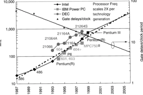
The importance of clocking has become even more emphasized, as the clock speed is rising rapidly, doubling every three years, as seen in Fig. 1.1. However, the clock uncertainties have not been scaling proportionally with the frequency increase, and an increasingly large portion of the clock cycle has been spent on the clocking overhead. The ability to absorb clock skew or to make the clocked storage element faster is reflected directly in the enhanced performance, since the performance is directly proportional to the clock frequency of a given system. Such performance improvements are very difficult to obtain using traditional tech- niques on the architecture or microarchitecture levels. The difficulties are caused by the overhead imposed by the CSE delay, and the clock uncertainties. Thus, setting the clock to the right frequency, and utilizing every available picosecond of the critical path, is increasingly important. It is our opinion that traditional clocking techniques will reach their limit when the clock frequency reaches the 5 to 10 GHz range. Thus, new ideas and new ways of designing digital systems are needed. We do not pretend to know what the future trend in clocking should
2 INTRODUCTION 3000 2500 - 6
Y
p
2000- 0 3 5 a,t"
1500-::
i52
1000- z Y-
-6
500 - 0 -I___ _--- ___l_l I~-
Pentiurn 4 Pentiurn 4 Athlon1900 Athlon210') Athlon 8 ltanlurn IBM-G4 PowerPC. *PM Athion Itanurn Alpha 21264 'PIII Xeon8 Alpha 21 164
Exponential
Alpha 21 164 IBM s1390 Alpha 21064 *Ultra wart 11 CraY-X-MP IBM 3090
Cray-1 s ~CDC-CYbeJ M1pS-X
-
<
1975 1980 1985 1990 1995 2000 2005
be, but we feel that some of the ideas discussed in this book can provide a good path to follow.
Computers built in the past were large and filled several electronic cabinets in large air-conditioned rooms that occupied entire A oors. They were built from discrete components or used a few large-scale integration (LSI) chips in the later models. Those systems were clocked at frequencies of about one or a few tens of megahertz, as shown in Table 1.1. The first electronic computer, ENIAC
(Electronic Numerical Integrator and Calculator), for example, operated at the maximal clock frequency of 18 kHz. Given the low scale of integration, it was possible to "tune" the clock. This was achieved by either adjusting the length of the wires that distributed the clock signals, or by tuning the various delay elements on the cabinets or the circuit boards, so that the clock signal arrived at every circuit board at approximately the same time. With the advent of very large- scale integration (VLSI) technology, and increased integration levels, the ability
to tune the clock has been greatly diminished. The clock signals are generated and distributed internally within the VLSI chip. Therefore, much of the burden of absorbing clock signal variations at various points on the VLSI chip has fallen
on the clocked storage element.
1 .l. CLOCKING IN SYNCHRONOUS SYSTEMS
The notion of clock and clocking is essential for the concept of synchronous design of digital systems. The synchronous system assumes the presence of the
CLOCKING IN SYNCHRONOUS SYSTEMS 3
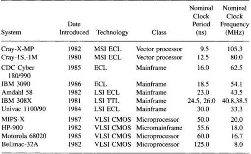
Table 1.1 Clock Frequency of Selected Historic Computers and Supercomputers Nominal Nominal
Clock Clock
Date Period Frequency
System Introduced Technology Class (ns) ( M W Cray-X-MP 1982 MSI ECL Vector processor 9.5
Cray- 1S,- 1 M 1980 MSI ECL Vector processor 12.5 CDC Cyber 1985 ECL Mainframe 16.0 IBM 3090 1986 ECL Mainframe 18.5 Amdahl 58 1982 LSI ECL Mainframe 23.0 IBM 308X 1981 LSI TTL Mainframe 24.5, 26.0 Univac 1100/90 1984 LSI ECL Mainframe 30.0 MIPS-X 1987 VLSI CMOS Microprocessor 50.0 HP-900 1982 VLSI CMOS Micromainframe 55.6 Motorola 68020 1985 VLSI CMOS Microprocessor 60.0 Bellmac-32A 1982 VLSI CMOS Microprocessor 125.0
Source: Wagner 1988. 180/990 outputs (Y)
+
Y= Y(X, S,) 105.3 80.0 62.5 54.1 43.5 40.8,38.5 33.3 20.0 18.0 16.7 8.0Figure 1.2. The concept of finite-state machine.
storage elements and combinational logic, which together make up a finite-state machine (FSM). The changes in the FSM are in general the result of two events: clock and input signal changes, as illustrated in Fig. 1.2.
The next state, & + I , is a function of the present state, S,, and the logic value
of the input signals: S,+l = &+I(&, X,). The remaining question is: When in time will FSM change to the next state, &+I. This change is determined by the
4 INTRODUCTION
type of clocked storage elements used and the clock signal. The function of the clock signal is to provide a reference point in time when the FSM changes from the present, S,,, to the next state,
In Fig. 1.3, we have implicitly assumed that the moment when the state changes from S,, to S,,+l is determined by the change in the clock signal from
logic “0” to logic “1.” In fact, this change is determined by the type of clocked storage element and its functionality. We will be discussing this point in detail later in this book. For the purposes of this discussion, we observe that without the clock signal, the change from S,, to Sn+l could not be precisely determined.
There are digital systems where this change is not caused by the presence, or more precisely, by a change in the clock signal, but by a change of the data signal, for example. Such systems are known as asynchronous systems, because they do not require the presence of the clock signal in order to effect an orderly transition from S,, to S,,+l. A great deal of research in defining a workable asynchronous
system has been done in the last several decades. Recently a microprocessor was designed to operate in an asynchronous manner, and it has been claimed that some small advantages in power consumption were obtained (Woods et al. 1997). In spite of that, the practicality and advantage of the asynchronous design has yet to be proven (Furber et al. 2001). In this book, we limit our discussion to synchronous systems.
If we extend the FSM state diagram in time, we obtain an illustration of the pipeline design (Fig. 1.3). In many cases, when dealing with the synchronous design, the delay throughout the logic block is excessive and the signal change cannot propagate to the inputs of the clocked storage elements in time to effect the change to the next state. In that case, the machine has not met the “critical- path requirement.” Such an FSM will fail in its functionality, because the changes
This process is illustrated in Fig. 1.3.
@ Time
CLOCKING IN SYNCHRONOUS SYSTEMS 5
initiated by the input signals will have no effect. This is because the time allowed to change to the next state, & + I , is too short and the input signal change does not
have sufficient time to propagate. In technical jargon this is known as critical-path violation. Critical path is defined as the chain of gates in the longest (slowest) path through the logic, which causes a signal to take a certain length of time to propagate from the input to the output. Often times, an additional state (or states) is inserted to assure that every transition proceeds in an orderly and timely fashion. This is known as pipelining. A diagram of a pipelined system is shown in Fig. 1.4.
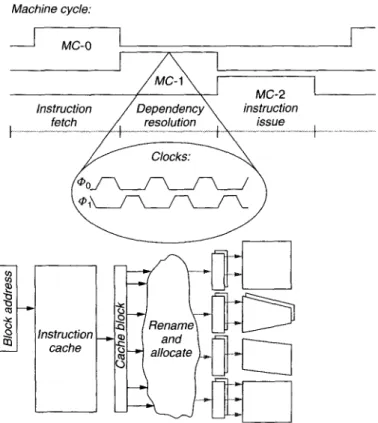
Several clock cycles may be needed in order for the signal to propagate through various stages of a computer system. In general, execution of an instruction may require several machine cycles, where machine cycle is defined as the time inter- val necessary for one atomic operation to execute an instruction. One machine cycle normally takes several clock cycles. The machine cycle is often designated by a waveform defining its own cycle. This is especially true if microcode is used to control the machine. In the past, microcoding was a popular concept and it was used extensively in Complex Instruction Set Computers (CISC). In those cases, a process of executing an instruction required several machine cycles. During each machine cycle one microinstruction was executed. It normally took several microinstructions to execute an instruction. Each machine cycle required one or several register transfers or passes through several pipeline stages. That in turn required one or more clock cycles, or multiple phases of the clock. Thus, the clocking was quite complex and encompassed several levels of hierarchy. This
6 INTRODUCTION
Machine cycle.
-
Figure 1.5. Machine execution phases with respect to the clock cycles.
is illustrated in Fig. 1.5, where three distinct machine cycles, Instruction Fetch, Dependency Resolution, and Instruction Issue, are shown. Dependency resolu- tion can be quite a complex operation, requiring several register transfers, which means several clock cycles are necessary to complete this operation (as shown in Fig. 1.5). The machine would normally scan the cache block for several instruc- tions and try to resolve any data dependencies. At the end of this cycle, operands will be fetched and placed in the corresponding registers (reservation stations) of the execution units.
In microcoded machines a large disparity existed between the speed of the clock and the speed of logic. It could take several clock cycles or even several tens or hundreds of clock cycles to execute one instruction. A more complex instruction required many more clock cycles. There could be tens of logic levels
in the critical path, and 40 to 50 were not uncommon. Thus, the time associated with the clock and clocking was not as critical as it is today.
As the level of integration increased, combined with the increased speed of today’s machines, the number of logic levels in the critical path started to diminish rapidly. Today’s high-speed processors are either implementing Reduced Instruc- tion Set Computer (RISC) architecture, or are running CISC code. However, to
CLOCKING IN SYNCHRONOUS SYSTEMS 7
be able to efficiently implement superscalar execution cores, even CISC com- puters are translating their instructions into simple RISC-type operations called ROPs (RISC operations). Their microarchitecture can execute one or several ROPs in place of one CISC instruction. Therefore, the concept of microcod- ing has disappeared, as did the concept of machine cycle when implementing a particular machine architecture. The instructions (or ROPs) are executed in one cycle, which is usually driven by a single-phase clock. In other words, one instruction (or one ROP) is executed in every clock cycle. The levels of hierarchy that existed between the clock cycle and instruction execution no longer exist. In addition, the number and depth of pipeline stages keeps increasing in order to accommodate the trend toward increasing speed. As a result, the number of logic stages between the two CSEs keeps decreasing. Today 10 levels of logic in the critical path are more common. This number is still decreasing, as illus- trated in Fig. 1.6. Any overhead associated with the clock system and clocking mechanism directly and adversely affects machine performance and is therefore critically important.
With this introduction we should be able to understand the function of the clock signal before we proceed with other definitions. The function of the clock signal is comparable to the function of the metronome in music. Similarly, in the digital system the clock designates the exact moment when the state is changing, as well as when the next state is to be captured. Also, all of the logic operations have to finish before the tick of the clock, because their final values are being captured by that clock event. Therefore, the clock provides the time reference point, which determines the flow of the data in the digital system.
Figure 1.6. Increase in the clock frequency and decrease in the number of logic levels in the pipeline. (Borkar 1999), Copyright 0 1999 IEEE.