Programming Specifications
CY8CMBR3xxx
Device Programming Specifications
Document No. 001-89944 Rev. *D
October 12, 2015
Cypress Semiconductor
198 Champion Court
San Jose, CA 95134-1709
Phone (USA): 800.858.1810
Phone (Intnl): 408.943.2600
http://www.cypress.com
Copyrights
License
© 2013-2015, Cypress Semiconductor Corporation. All rights reserved. This software, and associated documentation or materials (Materials) belong to Cypress Semiconductor Corporation (Cypress) and may be protected by and subject to world-wide patent protection (United States and foreign), United States copyright laws and international treaty provisions. Unless otherwise specified in a separate license agreement between you and Cypress, you agree to treat Materials like any other copyrighted item.
You agree to treat Materials as confidential and will not disclose or use Materials without written authorization by Cypress. You agree to comply with any Nondisclosure Agreements between you and Cypress.
If Material includes items that may be subject to third party license, you agree to comply with such licenses.
Copyrights
Copyright © 2013-2015 Cypress Semiconductor Corporation. All rights reserved.
PSoC® is a registered trademark and PSoC Creator™ is a trademark of Cypress Semiconductor Corporation (Cypress), along with Cypress® and Cypress Semiconductor™. All other trademarks or registered trademarks referenced herein are the property of their respective owners.
The information in this document is subject to change without notice and should not be construed as a commitment by Cypress. While reasonable precautions have been taken, Cypress assumes no responsibility for any errors that may appear in this document. No part of this document may be copied or reproduced in any form or by any means without the prior written consent of Cypress. Made in the U.S.A.
Disclaimer
CYPRESS MAKES NO WARRANTY OF ANY KIND, EXPRESS OR IMPLIED, WITH REGARD TO THIS MATERIAL, INCLUDING, BUT NOT LIMITED TO, THE IMPLIED WARRANTIES OF MERCHANTABILITY AND FITNESS FOR A PAR-TICULAR PURPOSE. Cypress reserves the right to make changes without further notice to the materials described herein. Cypress does not assume any liability arising out of the application or use of any product or circuit described herein. Cypress does not authorize its products for use as critical components in life-support systems where a malfunction or failure may rea-sonably be expected to result in significant injury to the user. The inclusion of Cypress’ product in a life-support systems appli-cation implies that the manufacturer assumes all risk of such use and in doing so indemnifies Cypress against all charges.
Flash Code Protection
Cypress products meet the specifications contained in their particular Cypress Data Sheets. Cypress believes that its family of PSoC products is one of the most secure families of its kind on the market today, regardless of how they are used. There may be methods that can breach the code protection features. Any of these methods, to our knowledge, would be dishonest and possibly illegal. Neither Cypress nor any other semiconductor manufacturer can guarantee the security of their code. Code protection does not mean that we are guaranteeing the product as “unbreakable.”
Cypress is willing to work with the customer who is concerned about the integrity of their code. Code protection is constantly evolving. We at Cypress are committed to continuously improving the code protection features of our products.
Contents
1. Introduction
5
1.1 Programmer ...5
1.2 Introduction to CY8CMBR3xxx ...6
2. Required Data
7
2.1 Hex File Origin ...72.2 Nonvolatile Subsystem ...7
2.3 Organization of the Hex File ...7
3. Communication Interface
9
3.1 The Protocol Stack ...93.2 I2C Interface ...9
3.3 Physical Layer ...10
3.4 Hardware Access Commands ...13
3.5 Pseudocode ...13
4. Programming Algorithm
15
4.1 High-Level Programming Flow ...154.2 Subroutines used in Programming Flow ...15
4.3 Step 1 – Acquire Chip ...18
4.4 Step 2 – Check Silicon ID ...21
4.5 Step 3 – Program Flash ...22
4.6 Step 4 – Verify Flash ...24
4.7 Step 5 – Release Chip ...25
A. Intel Hex File Format
26
B. I2C Protocol - Packets and Signals
27
B.1 Data Validity...281. Introduction
This programming spec gives the information necessary to program the nonvolatile memory of the CY8CMBR3xxx devices. It describes a communication protocol that an external programmer will access, explains the programming algorithm, and gives electrical specifications of the physical connection.
1.1
Programmer
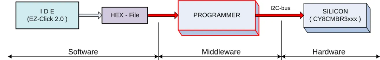
A programmer is a hardware-software system that stores a binary program (hexadecimal file) in the silicon's program (flash) memory. The programmer is an essential component of the engineer's prototyping environment or an integral element of the manufacturing environment (mass programming). The high-level diagram of the development environment is illustrated in
Figure 1-1.
Figure 1-1. Programmer in Development Environment
In the manufacturing environment, the IDE block is absent because its main purpose is to produce a hex file. As shown in Figure 1-1, the programmer performs three functions:
Parses the hex file; extracts necessary information Interfaces with the silicon as an I2C master
Implements the programming algorithm by translating the hex data into I2C signals
The structure of the programmer depends on its exploiting requirements. It can be software or firmware centric:
Software centric: The programmer's hardware works as a bridge between the protocol (such as USB) and I2C. All I2C com-mands are passed to the hardware through the protocol from an external device (software). The bridge is not involved in the parsing of the hex file and programming algorithm – the upper layer (software) performs this task. Examples of such program-mers are the Cypress MiniProg3 and TrueTouchBridge.
Firmware centric: This is an independent hardware design in which all the functions of the programmer are contained in one device, including storage for the hex file. Its main purpose is to be a mass programmer in manufacturing.
This document does not include the specific implementation of the programmer. It focuses on data flow, algorithms, and phys-ical interfacing.
It specifically covers the following topics, which correspond to the three functions of the programmer: Data to be programmed
Interface with the chip
Algorithm used to program the target device
PROGRAMMER SILICON
( CY8CMBR3xxx ) I D E
(EZ-Click 2.0 ) HEX - File
Software Middleware Hardware
Introduction
1.2
Introduction to CY8CMBR3xxx
The CY8CMBR3xxx family is an application-specific integrated circuit (ASIC) device for CapSense end applications. This device does not require any coding; instead, it has configuration registers that are programmed through an I2C-Bus.
The nonvolatile subsystem of the silicon consists of a flash memory system with a maximum of 128 bytes. The flash memory system stores the device configuration information.
The part can be programmed after it is installed in the system by way of the I2C interface (in-system programming). The char-acteristics of the I2C slave interface are:
Communication speed is up to 400 kHz. No bus stalling – no clock-stretching
The I2C address is configurable through the I2C register map.
This document focuses on the specific programming operations without referencing the silicon architecture. Many important topics are detailed in the Appendices. Most of the other material appears in the CY8CMBR3xxx datasheet.
The Appendices in this document are: Appendix A. Intel Hex File Format
Appendix B. I2C Protocol - Packets and Signals
Document Revision History
Document Title: CY8CMBR3xxx Device Programming Specifications Document Number: 001-89944
Revision Issue Date Origin of
Change Description of Change
** 11/06/2013 ANDI/LIRA New specification
*A 02/21/2014 ANDI/LIRA Remove CALC CRC and SAVE_CALC_CRC commands. Updated Figure 2-1.
*B 04/01/2014 ANDI/VVSK
Updated Section 4.1.
Corrected cross-reference in Section 4.3. Updated Pseudocode in Section 4.5. *C 06/30/2014 ANDI/BVI Corrected Figures 3-2 and 3-3. *D 10/12/2015 ANDI Updated Figure 4-4.
2. Required Data
This chapter describes the information that the programmer must extract from the hex file to program the CY8CMBR3xxx silicon.
2.1
Hex File Origin
Customers use the EZ-Click GUI to develop their projects. After the project development, the nonvolatile configuration of the silicon is saved in the hex file. Only one record in this file actually targets the flash memory:
Device configuration registers
Other records are auxiliary and are used to keep the integ-rity of the programming flow.
2.2
Nonvolatile Subsystem
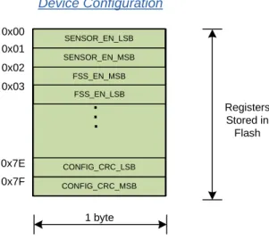
The flash memory is organized into one bank of 128 bytes. The programming granularity is one bank at a time.
The bank represents the registers of the Device Configura-tion state. During the silicon's start-up (after HW/SW reset), the re-programmed functionality is loaded into the corre-sponding volatile memory (registers).
Figure 2-1 shows the flash organization and how it maps to the I/O space of the silicon.
Figure 2-1. Nonvolatile Subsystem
The flash memory is mapped directly to the I/O registers of the silicon; 128 bytes of flash configure 0x00-0x7F registers of the Device Configuration state. Programmer extracts all 128 bytes from the hex file.
For more information about registers and operating states, refer to the CY8CMBR3xxx datasheet.
2.3
Organization of the Hex File
The hexadecimal (hex) file is a medium to describe the non-volatile configuration of the project. It is the data source for the programmer.The hex file for the CY8CMBR3xxx family follows the Intel Hex File format. Because Intel's specification is generic, it defines only some types of records that can make up the hex file. The specification allows customizing the format for essentially any possible silicon architecture. The functional meaning of the records is defined by the silicon vendor and typically varies for different chip families. See Appendix A: Intel Hex File Format on page 26 for details of the Intel Hex File Format.
The CY8CMBR3xxx family defines three types of data sec-tions in the hex file: configuration flash, checksum, and metadata. See Figure 2-2 to determine the allocation of these sections in the address space of the Intel Hex File. The address space of the hex file does not map to the phys-ical addresses of the I/O registers of the silicon. Program-mer uses hex addresses (see Figure 2-2) to read sections from the hex file into its local buffer. Later, this data is pro-grammed (translated) into the corresponding addresses of the silicon. Device Configuration Registers Stored in Flash 1 byte 0x00 0x01 0x7F 0x7E 0x02 FSS_EN_MSB CONFIG_CRC_MSB CONFIG_CRC_LSB
..
.
SENSOR_EN_LSB SENSOR_EN_MSB FSS_EN_LSB 0x03Required Data
Figure 2-2. Organization of Hex File for the CY8CMBR3xxx Family
0x0000 0000 - Configuration Data (128 bytes), which must be programmed into the flash. These bytes configure the CY8CMBR3xxx device during boot.
0x9030 0000 - Checksum (2 bytes) of all the bytes in the Configuration Flash (128 bytes). The checksum is the arith-metical sum of every byte in the user's flash. The 2-byte result is saved in this section in the Big-Endian format (MSB byte is first). This record must be used by the programmer to check the integrity of the hex file. Integrity means that the "Checksum" and "Configuration Flash" sections must corre-late in this file.
0x9050 0000 - Meta Data (7 bytes). This section contains data, which is not programmed into flash. These are param-eters for the programmer used during programming. The meaning of the fields in this section are listed in Table 2-1.
Table 2-1. Meta Data in Hex File
Hex file version: This 2-byte field in Cypress's hex-file defines its version (or type). The version for the CY8CMBR3xxx family is "0x0101". The programmer should use this field to check if the provided file corre-sponds to the target device, or to select the appropriate parsing algorithm if it supports some families.
I2C Write Address: This I2C address must be used dur-ing the programmdur-ing step. Note that after the device is programmed by this file, its I2C address can be changed (the new address is effective only after a reset or power cycle). Therefore, during the second and next program-ming cycles, the programmer must use the I2C Verify Address. This field makes sense for the first program-ming cycle.
I2C Verify Address: Use this I2C address during the ver-ification step. Note that after the first programming cycle, the I2C Write and I2C Verify addresses will be the same. The correct use of the I2C Write and I2C Verify
addresses will be covered later in this document. Device ID: This three-byte value defines the part number
for which this hex file is generated. These three bytes reflect the content of FAMILY_ID and DEVICE_ID[0-1] registers in the memory map. For example, for
CY8CMBR3002 the Device ID is "0x9A (family_id), 0x0A (silicon_id_high), 0x00 (silicon_id_low)". The program-mer uses this field to check whether the hex file corre-sponds to the target chip. See Table 2-2 to understand the correspondence between the ID in hex and the memory map.
Offset Data Type Length in Bytes
0x00 Hex file version 2 (big-endian) 0x02 I2C write address 1 0x04 Device ID (High) 1 0x05 Device ID (Low) 1 0x06 Device ID (Family) 1 0x0000 0000 128 bytes 0x9030 0000 2 bytes 0x9050 0000 7 bytes Configuration Flash Checksum Metadata N Bytes
- unused space - populated space
Table 2-2. Device ID in Hex and Memory Map
I2C Register Device ID
(in hex) Description
0x91 Meta Data [4] High ID 0x90 Meta Data [5] Low ID 0x8F Meta Data [6] Family ID
3. Communication Interface
This chapter explains the low-level details of the communi-cation interface.
3.1
The Protocol Stack
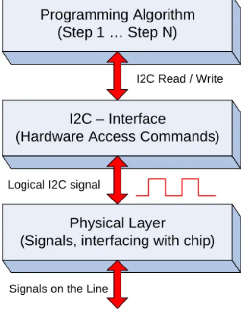
Figure 3-1 illustrates the stack of protocols involved in the programming process. The programmer must implement both hardware and software components.
Figure 3-1. Programmer’s Protocol Stack
The Programming Algorithm protocol—the topmost proto-col—implements the whole programming flow in terms of atomic I2C commands. It is the most solid and fundamental part of this specification. For more information on this algo-rithm, see Chapter 4: Programming Algorithm.
The I2C Interface and Physical Layer are the lower-layer protocols. Note that the physical layer is the complete hard-ware specification of the signals and interfacing pins, and includes drive modes, voltage levels, resistance, and other components. The upper protocols are logical and algorith-mic levels.
The purpose of the I2C interface layer is to be a bridge between pure software and hardware implementations. The “Programming Algorithms” protocol is implemented com-pletely in the software; its smallest building block is the I2C command. The whole programming algorithm is the mean-ingful flow of these blocks. The I2C interface helps to isolate the programming algorithm from hardware specifics, which makes the algorithm reusable. The I2C interface must trans-form the software representation of these commands into line signals (digital form).
3.2
I2C Interface
Inter-Integrated Circuit (I2C) is the industry-standard com-munication interface developed by Phillips Semiconductors (now NXP Semiconductors). It is a synchronous, serial, 8-bit oriented, bidirectional 2-wire bus that implements a master/ slave relationship with 128 slaves on the bus. The I2C stan-dard defines the following working modes: Stanstan-dard (up to 100 kHz), Fast (up to 400 kHz), Fast-mode + (up to 1 MHz), or High Speed (up to 3.4 MHz). The complete bus specifica-tion can be found on the official NXP website. Designers of I2C-compatible chips must use the I2C-Bus specification and user manual (UM10204) as a reference to ensure that their devices meet all specific limits.
Cypress's family of CY8CMBR3xxx devices is I2C-compati-ble and these devices operate in the slave mode. The mas-ter (host) uses an I2C bus to program flash or configure devices during runtime, read CapSense data, and so on. The third-party programmer of the CY8CMBR3xxx device must implement the I2C master according to the standard specification. The developer of Programmer will probably use any available solution of the master, which passed the test for compliance with the I2C specification. Such ICs are produced by more than 50 companies around the globe. Programming Algorithm
(Step 1 … Step N)
I2C – Interface
(Hardware Access Commands)
Physical Layer (Signals, interfacing with chip)
I2C Read / Write
Logical I2C signal
Communication Interface
Note that the programmer may occasionally need to work in a multi-master environment. Consider that possibility when selecting the master's solution. In most cases, programming runs on single-master buses.
The CY8CMBR3xxx I2C interface has the following fea-tures:
7-bit addressing mode (up to 128 slaves). Bit-rate up to 400 kHz (Standard mode). No bus stalling – no clock stretching.
I2C buffer – 252 bytes (the first 128 bytes are used for device configuration).
The developer of programmer must ensure that the selected or designed solution of the I2C master supports all these features, which are a subset of the I2C specification.
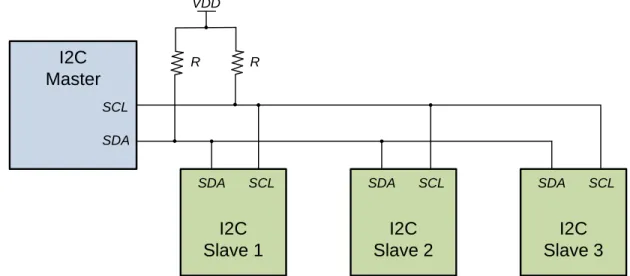
The I2C-Bus defines two digital pins to communicate with the master (programmer). They are sufficient for bidirec-tional, semi-duplex data exchange (byte granularity). These two bidirectional wires are:
Serial Clock (SCL): This line is used to synchronize the slave with the master.
Serial Data (SDA): This line is used to send data between the data and slave.
Figure 3-2 shows an example of an I2C bus with slaves. Note During programming of the CY8CMBR3xxx device, the I2C bus executes only the transport function (sends bytes between the master and slave). A complete set of lines is required from the programmer to communicate with the CY8CMBR3xxx device, as specified in Physical Layer.
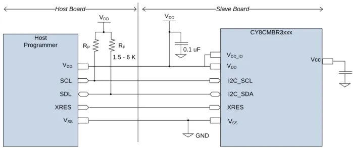
Figure 3-2. I2C Bus Connection Schematic
The programming flow consists of multiple Read and Write I2C transactions. These transactions are atomic transac-tions from the standpoint of this specification. They can be of different length in bytes, but both are embraced in the bus's START and STOP signals. Repeated START is not used.
See Appendix B: I2C Protocol - Packets and Signals on page 27 to understand the structure of the Read/Write trans-actions and their waveforms on the bus.
3.3
Physical Layer
This section describes the hardware connections between the programmer and the target device for programming. It shows the connection schematic and gives information on electrical specifications.
The external interface connection between the host pro-grammer and the target CY8CMBR3xxx device is shown in
Figure 3-3 on page 11.
This figure also depicts all the power supply connections required in the typical working conditions of chip.
I2C
Master
SCL SDAI2C
Slave 1
SCL SDAI2C
Slave 2
SCL SDAI2C
Slave 3
SCL SDA VDD R RCommunication Interface
Figure 3-3. Connection Schematic of Programmer
Only five pins are required to communicate with the chip. Note that the SCL and SDA pins are only required by the I2C protocol.
The optional HW Reset (XRES) pin may be used to reset the slaves. This pin is used if the device is stuck or to clear the I2C bus (when SCL is stuck LOW, which is unlikely to occur). It is used to reset the part as a first step in a pro-gramming flow.
You can program a chip in the Reset, No-Reset, or Power Cycle mode. The mode defines only the first step—how to acquire the part—in the programming flow. The other steps are identical (I2C traffic).
Reset mode – To start programming, the host toggles the XRES line, and then sends the I2C commands. In this case, the power on the target board can be supplied by the host or by an external power adapter (the VDD line can be optional).
No-Reset mode – In this mode, the host must be sure that power is supplied to the target board via an external adaptor or from the host. Then, it can generate I2C traf-fic immediately. The XRES line is not used and the VDD connection can also be optional if the target is powered
by an external source. This method has a drawback – the chip is not reset before programming. This method will fail if the I2C bus or device is stuck.
Power Cycle mode – To start programming, the host powers on the target and then starts sending the I2C commands. The XRES line is not used.
It is recommended that the programmer uses all five pins and supports at least the Power Cycle mode of program-ming. The Reset mode support is optional.
Most of the packages of the CY8CMBR3xxx device do not have an XRES pin. For them, the programmer will use the No-Reset or Power Cycle modes.
Host Programmer CY8CMBR3xxx VDD VDD SCL XRES SDL I2C_SCL XRES I2C_SDA VDD GND VSS 0.1 uF VSS RP RP 1.5 - 6 K VDD Vcc
Host Board Slave Board
VDD_IO
Note 1: The VDD_IO supply is pin available only the selected packages. For the packages that have a VDD_IO pin, the VDD and VDD_IO pins should be connected together (shorted) on the board.
Note 2: Acceptable range for VDD is 1.8 V ±5% and 2 V to 5.5 V.
Note 3: If the device is powered in the 1.8 V ±5% range, the VDD and VCC pins must be connected together (shorted) on the board. If the device package has a VDD_IO pin, then the VDD, VDD_IO, and VCC must be connected together (shorted).
Note 4: All other pins which are not shown in the circuit above should not be connected to any electrical node and must be left floating.
Communication Interface
Table 3-1. Programming Mode
Table 3-2. CY8CMBR3xxx Pin Names and Requirements
Mode Necessary Pins Unused
Pins Use cases
Reset VDD (optional) GND XRES SCL SDA VDD (if self-pow-ered)
1. Board can be self-powered (device VDD is not connected to the programmer). 2. This mode is used when the board consumes too much current, which the pro-grammer cannot supply (VDD line is not connected).
3. Five-pin case – when the host supplies power and toggles XRES (this is the most popular programming method).
4. If there are other devices on the I2C bus, it is recommended to connect the host’s XRES to every chip. It will ensure that the host can reset every slave that may hang up the bus.
No-Reset VDD (optional) GND SCL SDA VDD (if self-pow-ered and no XRES)
1. The board can be self-powered (device VDD is not connected to the program-mer).
2. This mode is used when the board consumes too much current, which the pro-grammer or the I2C master cannot supply (the VDD line is not connected). 3. This mode is used when the I2C master (host) or slave (target) does not have an XRES pin. Power Cycle VDD GND SCL SDA XRES
1. This mode is used when the I2C master (host) or slave (target) does not have an XRES pin on the part’s package. The only way to reset a part is the Power Cycle mode when there is no XRES pin.
2. The Power Cycle mode is relevant to most of the CY8CMBR3xxx packages because all of them, except one, do not have an XRES pin. It is the recommended mode.
3. Some third-party I2C masters can use this mode if they do not implement the XRES line but can supply power (on/off) to reset a part.
CY8CMBR3xxx
Pin Name Function External Programmer – Drive Modes
VDD Power supply input
(1.8 – 5.5 V) Positive voltage – powered by external power supply or by programmer. VSS Power supply return Low resistance ground connection. Connect to circuit ground.
XRES Active low external reset input
(with internal pull up). Output – drive TTL levels (Drive mode – Strong)
SCL I
2C Clock line
(up to 100 kHz)
Output – drive TTL levels (Drive mode – Open Drain Low) Input – read TTL levels in High-Z mode.
In general, SCL is bidirectional to watch for clock-stretching but CY8CMBR3xxx devices do not support stretching. Therefore, this line is used in the unidirectional mode.
The external pull-up resistor (RP) must be calculated.
SDL I
2C Data line
- bidirectional
Output – drive TTL levels (Drive mode – Open Drain Low) Input – read TTL levels in High-Z mode.
The external pull-up resistor (RP) must be calculated.
VCC Power Output Filter The external 0.1-uF capacitor must be connected between this pin and ground. CMOD External Modulator Capacitor The external 2.2-nF capacitor must be connected between this pin and ground.
Communication Interface
Figure 3-3 on page 11 shows that the I2C bus requires external pull-up resistors (RP). In choosing these resistors, consider supply voltage, clock speed, and bus capacitance. The typical value is in the range of 1.5 to 6 K for supply voltages in the range of 1.8 to 5.0 V. More information about calculating the RP value can be found in the I2C Bus Speci-fication (UM10204, section 7.1 - Pull-up resistor sizing). The I2C timing specifications and the silicon's electrical specifications are documented in the CY8CMBR3xxx data-sheet.
3.4
Hardware Access
Commands
This section focuses on the low-level APIs that must be sup-ported by the programmer of the CY8CMBR3xxx devices. The APIs must be implemented by the I2C Interface layer shown in Table 3-3. They make up the software fundamental for the high-level programming algorithm. This low-level API interface can be considered the hardware abstraction layer, because it is hardware-independent (but its implementation is important for concrete hardware). Theoretically, the upper layer (Programming Algorithm in Table 3-3) can be reused for a different programmer hardware.
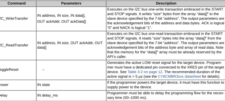
Table 3-3 lists the hardware access commands used by the software layer.
Table 3-3. Hardware Access Commands
For more information on the structure and waveform of the Read/Write I2C transactions, see Appendix B: I2C Protocol - Packets and Signals on page 27.
3.5
Pseudocode
The programming flow consists of numerous I2C_Read and I2C_Write transfer commands, with multiple status acknowl-edgement bits that must be checked every time. It is conve-nient to wrap them up in new procedures. This document uses easy-to-read pseudocode to show the programming algorithm.
The following two commands are used for the programming script:
I2C_Write (address, size, data[]) I2C_Read (address, size, OUT data[])
where the address, size, and data[] parameters have the same meaning as in the corresponding I2C_Read and I2C_Write transfer commands (see Table 3-3). The upper-layer APIs automatically check all ACKs of current transac-tion and return a single status via its name. These APIs help to keep the programming script concise. The following are some usage examples:
BYTE[3] data = {0x07, 0x25, 0xAF} I2C_Write( 0x04, 3, data)
BYTE[10] data; //reserve 10 bytes I2C_Read ( 0x04, 10, OUT data)
Command Parameters Description
I2C_WriteTransfer IN address, IN size, IN data[], OUT ackAddr, OUT ackData[]
Executes on the I2C bus one-write transaction embraced in the START and STOP signals. It writes “size” bytes from the array “data[]” to the slave device specified by the 7-bit “address”. The output parameters are the acknowledgement bits of the address and data bytes. ACK is logical “0” and NACK is logical “1”.
I2C_ReadTransfer IN address, IN size, OUT ackAddr, OUT data[]
Executes on the I2C bus one-read transaction embraced in the START and STOP signals. It reads “size” bytes into the array “data[]” from the slave device specified by the 7-bit “address”. The output parameters are acknowledgement bits of the address byte and array of read data. Note that the memory for the “data[]” array must be already reserved by the API’s caller.
ToggleReset –
Generates the active LOW reset signal for the target device. Program-mer must have a dedicated pin connected to the XRES pin of the target device. See Table 3-2 on page 12. The recommended duration of the active signal is > 5 µs (see the CY8CMBR3xxx datasheet for details). Power IN state If the programmer powers the target device, it must have this function to
supply power to the device.
Delay IN delay_ms Programmer must be able to delay the programming flow for the neces-sary time (50–1000 ms).
Communication Interface
The defined Write and Read pseudo-commands must be successful if they return the ACK status for every written byte. For Read transactions, this is the ACK of only the address byte, but for the Write transaction address and all data bytes, it must be ACKed. If at least one byte is NACKed, the transaction is treated as failed. In this case, depending on the programming context, the process must be terminated or the transaction tried again.
The following is the implementation of Write/Read pseudo-commands based on hardware access commands (Table 3-3): bool I2C_Write (address, size, data[])
{
BYTE ackAddr;
BYTE[size] ackData; //reserve space for status bytes of data //1 bit is sufficient for 1 ACK
//This implementation uses byte to store 1 ACK bit
I2C_WriteTransfer (address, size, data[], OUT ackAddr, out ackData);
// Check ACKs of address and data bytes (ACK = 0x00, NACK = 0x01)
If (ackAddr != 0x00) Return FALSE; //NACK
For (BYTE i = 0; i < size; i++) {
If (ackData[i] != 0x00) Return FALSE; //NACK
}
Return TRUE; //all ACKed
}
bool I2C_Read (address, size, OUT data) {
BYTE ackAddr; //reserve 1 bit (byte in fact) for ACK bit of address byte //assuming that “size” bytes for “data” is allocated by caller
I2C_ReadTransfer (address, size, OUT ackAddr, OUT data);
If (ackAddr != 0x00) Return FALSE; //NACK
Return TRUE; //ACK
}
The programming code in Chapter 4: Programming Algorithm, will be based mostly on the I2C_Write/Read pseudo-com-mands and some compseudo-com-mands from Table 3-3.
4. Programming Algorithm
This chapter describes the programming flow of the CY8CMBR3xxx device. It starts with a high-level description of the algorithm and then describes every step using the pseudocode. All programming script is made up of hardware access commands (see “Hardware Access Commands” on page 13).
Atomic I2C_Read/Write() APIs from “Pseudocode” on page 13. They are middle-level APIs.
High-Level subroutines, which wrap up atomic I2C_Read/Write() APIs. They make up ~ 90% of the whole script. See Subroutines used in Programming Flow.
It is possible to write the entire script using the hardware access commands. In that case, the script is enormous and will have a lot of duplication. This approach causes signifi-cant inconvenience in studying the script and its support. The purpose of high-level APIs (pseudocode) is to make the script easy to read and eventually mappable on the actual programming language.
4.1
High-Level Programming
Flow
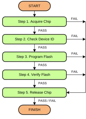
Figure 4-1 shows the sequence of steps that must be exe-cuted to program the CY8CMBR3xxx device. These steps are described in the following sections. All of the steps in this programming flow must be completed for a successful programming operation. The programmer should stop the programming flow if any step fails. In addition, in pseudo-code, it is assumed that the programmer checks the status of each I2C transaction (I2C_Write, I2C_Read, WritePacket, ReadPacket). This extra code is not shown in the program-ming script.
If any of these transactions fails, you must abort program-ming. To abort, execute Step 5 – Release Chip, which exe-cutes the opposite actions of Step1. It ensures that the programmer and the target are left in the known state after programming is stopped (upon PASS or FAIL).
The flash programming in the CY8CMBR3xxx family is implemented by accessing its registers through the I2C bus.
The external programmer puts parameters into the volatile memory and requests a system call, which, in turn, performs flash updates.
Figure 4-1. High-Level Programming Flow of CY8CMBR3xxx Device
4.2
Subroutines used in
Programming Flow
The programming flow includes some operations that are intensively used in all the steps. Eventually, the program-ming code will look compact and easy-to-read and under-stand. Besides that, most registers and frequently-used constants are named and referred to from the pseudocode.
Step 1. Acquire Chip
Step 3. Program Flash
Step 4. Verify Flash
Step 5. Release Chip START
FINISH Step 2. Check Device ID
FAIL FAIL FAIL FAIL PASS PASS PASS PASS PASS / FAIL
Programming Algorithm
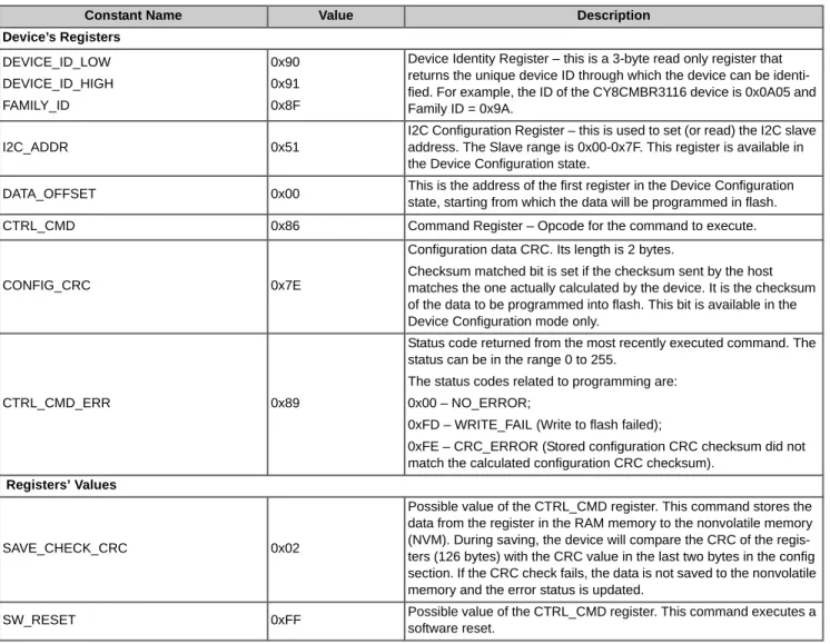
Table 4-1. Constants Used in Programming Script
Table 4-2. Subroutines used in Programming Flow
Constant Name Value Description
Device’s Registers DEVICE_ID_LOW DEVICE_ID_HIGH FAMILY_ID 0x90 0x91 0x8F
Device Identity Register – this is a 3-byte read only register that returns the unique device ID through which the device can be identi-fied. For example, the ID of the CY8CMBR3116 device is 0x0A05 and Family ID = 0x9A.
I2C_ADDR 0x51
I2C Configuration Register – this is used to set (or read) the I2C slave address. The Slave range is 0x00-0x7F. This register is available in the Device Configuration state.
DATA_OFFSET 0x00 This is the address of the first register in the Device Configuration state, starting from which the data will be programmed in flash. CTRL_CMD 0x86 Command Register – Opcode for the command to execute.
CONFIG_CRC 0x7E
Configuration data CRC. Its length is 2 bytes.
Checksum matched bit is set if the checksum sent by the host matches the one actually calculated by the device. It is the checksum of the data to be programmed into flash. This bit is available in the Device Configuration mode only.
CTRL_CMD_ERR 0x89
Status code returned from the most recently executed command. The status can be in the range 0 to 255.
The status codes related to programming are: 0x00 – NO_ERROR;
0xFD – WRITE_FAIL (Write to flash failed);
0xFE – CRC_ERROR (Stored configuration CRC checksum did not match the calculated configuration CRC checksum).
Registers’ Values
SAVE_CHECK_CRC 0x02
Possible value of the CTRL_CMD register. This command stores the data from the register in the RAM memory to the nonvolatile memory (NVM). During saving, the device will compare the CRC of the regis-ters (126 bytes) with the CRC value in the last two bytes in the config section. If the CRC check fails, the data is not saved to the nonvolatile memory and the error status is updated.
SW_RESET 0xFF Possible value of the CTRL_CMD register. This command executes a software reset.
Subroutine Description
bool WritePacket( address, size,
data[] )
This subroutine wraps I2C_Write() API from the “Pseudocode” on page 13. It keeps sending the same I2C write request until it is ACKed. If the CY8CMBR3xxx does not respond (NACKs), then the master has to poll it for some time.
bool ReadPacket( address,
size, OUT data[])
This subroutine wraps the I2C_Read()API from the “Pseudocode” on page 13. It keeps send-ing the same I2C read request until it is ACKed. If the CY8CMBR3xxx device is unresponsive on the I2C bus, the master has to try sometimes.
Programming Algorithm
The implementation of these subroutines follows. It is based on the pseudocode and registers defined in “Pseudocode” on page 13 and “Hardware Access Commands” on page 13. It uses the constants defined in this chapter.
The pseudocode is similar to a C-style notation.
// “WritePacket” Subroutine
bool WritePacket ( address, size, data[] ) {
bool ack;
for (i = 0; i < 20; i++) {
ack = I2C_Write(address, size, data[]); if (ack) // ACK
{
return TRUE ; }
}
return FALSE; // NACK
}
// “ReadPacket” Subroutine
bool ReadPacket (address, size, OUT data[]) {
bool ack;
for (i = 0; i < 20; i++) {
ack = I2C_Read(address, size, OUT data[]); if (ack) // ACK
{
return TRUE ; }
}
return FALSE; // NACK
Programming Algorithm
4.3
Step 1 – Acquire Chip
The first step in the programming flow is to ensure that the device is detected on the bus and is ready for programming. The acquisition algorithm is tricky for the CY8CMBR3xxx device. Besides initialization, determine the I2C address from the hex file you need to use: Program or Verify address (see “Organization of the Hex File” on page 7). This address is programmable in the CY8CMBR3xxx devices and it can be changed after a successful programming cycle. Note that the Program and Verify addresses are configurable in the EZ-Click GUI. If you need to change them, update your project and regenerate the hex file. The following programming scenarios are possible:
The target is only from the factory and will be programmed the first time (and probably the last time) for the end design. It is mass production programming. In this case, the hex file will have the correct "I2C Program Address" that matches the actual address of the target chip. Cypress will ship these devices with the default factory configuration where the I2C address is 0x37.
The target is programmed the second time, and subsequently, using hex files with the same Program and Verify
addresses. This is the prototyping scenario or flash upgrade in the field. In this case, the device will boot up with the Verify address (programmed last time). Therefore, it is necessary to use this address for both the Program and Verify opera-tions.
In general, the hex file must reflect the correct Program and Verify addresses of the target chip. The end design must avoid the following ambiguous scenarios on the bus:
Two slaves with the same addresses as the corresponding fields in the hex file (I2C Program and Verify addresses). In this case, the target device may not be detected correctly (especially if both are from the CY8CMBR3xxx family).
After the programming step, a new target's address has a conflict with the other device on the bus. Theoretically, this case should fail during verification step.
The Acquire step programmer determines the correct I2C address to be used during the next two steps: "Check Device ID" and "Program Flash". In the "Verify Flash" step, the Verify address from the hex file is always used.
Figure 4-2 shows the acquire algorithm. It is assumed that the programmer starts acquisition from one of the three modes described in the section Physical Layer – Reset, No-Reset or Power Cycle.
Programming Algorithm
Figure 4-2. Flow Chart of Acquisition Sequence
XRES Toggle or Power Cycle START
Return FAIL
NO Read 1 byte from “Program Address”
ACKed ?
YES
NO
Timeout >= 3 sec Read 1 byte from “Verify Address”
ACKed ? Detected_Address = Program_Address YES Detected_Address = Verify_Address NO NO Return FAIL YES Check if detected device is from CY8CMBR3xxx
family. Read I2C_ADDR register, its content must be the same as Detected_Address.
I2C_ADDR == Detected_Address
Return PASS
Programming Algorithm
Pseudocode – Step 1. Acquire Chip
/ /---// Note, that this step requires following data from hex-file:
// - I2C Program Address (0x90500002 – offset in hex) // - I2C Verify Address (0x90500003 – offset in hex) // Programmer should implement below APIs:
// 1) HEX_GetProgramAddr() and 2) HEX_GetVerifyAddr()
// Reset Target depending on acquire mode – Reset or Power Cycle
If (AcquireMode == “Reset”) ToggleReset(); // Toggle XRES pin, target must be powered.
Else If (AcquireMode == “Power Cycle”) Power(ON);// Supply power to target. // Loop to find out correct I2C device from hex-file
Program_Address = HEX_GetProgramAddr(); Verify_Address = HEX_GetVerifyAddr(); Do
{
ack = ReadPacket (Program_Address, 1, out data); If (ack == ACK)
{
Detected_Address = Program_Address; // to be used in Steps 2,3
break; }
ack = ReadPacket (Verify_Address, 1, out data); If (ack == ACK)
{
Detected_Address = Verify_Address; // to be used in Steps 2,3
break; }
}
While (time_elapsed < 3 sec);
If (time_elapsed >= 3 sec) Return FAIL;
//Check if device belongs to CY8CMBR3xxx family
//Read I2C_ADDR register and compare it with Detected_Device. They must match.
data[0] = I2C_ADDR;
WritePacket(Detected_Address, 1, data); ReadPacket(Detected_Address, 1, out data); If (data[0] != Detected_Address) Return FAIL; Return PASS;
//---Programming Algorithm
4.4
Step 2 – Check Silicon ID
This step is required to verify that the acquired device corresponds to the hex file. It reads the ID from the hex file and com-pares it to the ID obtained from the target.
Figure 4-3. Flow Chart of Check Silicon ID
Pseudocode – Step 2. Check Silicon ID
//---// Read “Device ID” from Hex-file - 3 byte from address 0x9050 0004.
// HEX_ReadDeviceID() must be implemented. // “Detected_Address” is taken from Step 1.
HexID = HEX_ReadDeviceID();
//Checking Device ID register – Low and High bytes
data[0] = DEVICE_ID_LOW;
WritePacket ( Detected_Address, 1, data); ReadPacket(Detected_Address, 2, out data);
IF ((HexID[0] != data[1]) || (HexID[1] != data[0])) Return FAIL;
//Checking Family ID register
data[0] = FAMILY_ID;
WritePacket ( Detected_Address, 1, data); ReadPacket(Detected_Address, 1, out data); IF (HexID[2] != data[0])
Return FAIL; Return PASS;
//---START
Read Device and Family IDs from HEX
Read Device ID from target (read DEVICE_ID register)
Chip Family ID == Hex Family ID
YES
Return PASS Return FAIL
NO Chip Device ID ==
Hex Device ID ?
NO
Read Family ID from target (read FAMILY_ID register)
Programming Algorithm
4.5
Step 3 – Program Flash
Programming of the flash memory of the CY8CMBR3xxx device is straightforward. Load the configuration data (128 bytes) into the volatile memory and commit program. This request programs whole flash and generates a software reset to reload the new configuration.
The source data is extracted from the hex file starting from address 0x00000000 (see Figure 4.4). Note that the flash size of the acquired silicon must be equal to the size of the configuration data in the hex file. This was ensured in Step 2 – Check Sil-icon ID by comparing the Device IDs of the hex and the target. The following figure illustrates this programming algorithm.
Figure 4-4. Algorithm of "Program Flash" Step
Pseudocode – Step 3. Program Flash
//---// Configuration data must be extracted from hex-file (address 0x0000 0000). For that: // HEX_ReadData(offset, length) API must be implemented.
// “Detected_Address” is taken from Step 1.
//1. Extract 128 configuration bytes from the hex file byte[] HexData = Hex_Readdata(0,128);
//2. Prepare I2C buffer with configuration data
START
Save Device Configuration in volatile memory
If Error Code == 0x00 ?
YES
NO
Return FAIL Send SW Reset Command
Return PASS
Send configuration data to volatile memory
Get Execution Status Send Command to program device’s
configuration in Flash
Programming Algorithm
byte[] data = new byte[129]; data[0] = DATA_OFFSET;
for (int i = 0; i < 128; i++) data[i+1] = HexData[i]);
//3. Write configuration into volatile memory WritePacket(Detected_Address, 129, HexData);
//4. Save Device Configuration (128 byte)
data[0] = CTRL_CMD; data[1] = SAVE_CHECK_CRC;
WritePacket(Detected_Address, 2, data);
//5. Read register that contains status of last executed command
data[0] = CTRL_CMD_ERR;
WritePacket(Detected_Address, 1, data);
Delay(300); //wait until flash update is complete, max 220 ms ReadPacket(Detected_Address, 1, out data);
If (data[0] != 0x00)
Return FAIL; //Failed to program configuration //6. Executes the software reset
data[0] = CTRL_CMD; data[1] = SW_RESET;
WritePacket(Detected_Address, 2, data);
//7. Wait time until reloading is complete (e.g. 100 ms)
Delay(100);
Programming Algorithm
4.6
Step 4 – Verify Flash
This is mandatory for the programmer because no other method ensures that the written data is correct (for example, check-sum). Because checksum cannot guarantee that all data in flash is identical to the hex content, each flash byte must be checked separately.
The verification process starts from reading device configurations from the chip and compares it with the corresponding hex data. If there are any differences, the programmer must stop and return fail. The programmer reads the new data not directly from flash, but from the same volatile buffers that were used during programming (see Figure 2-2 on page 8). New flash data was automatically loaded there at the end of the programming step. This data must be identical to the flash's content, since "nobody" tried to change it between the Program and Verify steps.
Figure 4-5. Algorithm of “Verify Flash” Step
Pseudocode – Step 4. Verify Flash
//---// Configuration data must be extracted from hex-file (address 0x0000 0000).
// The I2C address for verification is extracted from hex-file (address 0x9050 0003) // 2 HEX APIs are used in this step: HEX_ReadData() and HEX_GetVerifyAddr()
Verify_Address = HEX_GetVerifyAddr();
//1.Read Configuration Data from the Registers
data[0] = DATA_OFFSET;
WritePacket(Verify_Address, 1, data); ReadPacket(Verify_Address, 128, out data);
//2. Extract 128 bytes from hex-file from offset 0x00000000
byte[] hex_Data = HEX_ReadData(0, 128);
//3. Compare hex vs chip data
for (int i = 0; i < 128; i++) {
if (hex_Data[i] != data[i]) return FALSE; }
return PASS;
START
Read Device Configuration from chip
Read Device Configuration from hex
Chip Device Config == Hex Device Config ?
YES
Return PASS Return FAIL
Programming Algorithm
4.7
Step 5 – Release Chip
This step, which is the opposite of Step 1 – Acquire Chip, releases the chip from the programmer. The programmer executes the final actions, such as power-down or reset, disconnecting from the I2C bus (putting lines into the high-Z state), and so on. After this step, the programmer can be disconnected from the chip. For example, on an automated pipeline, the chip in the socket is replaced by the next part. Therefore, the programmer can start again from Step 1 – Acquire Chip.
It is recommended to call this step at the end of the programming flow and even after failed steps. Therefore, we can ensure that in the end, the device is in the known state.
This step is optional and does not generate any I2C traffic, but guarantees that the programmer and the target are left in the known state at the end of programming.
Pseudocode – Step 5. Release Chip.
//---// This step depends on the power source. Whether target powered by Programmer or // external source.
// 1.Power Off or Reset device
Power (OFF) // if powered by Programmer
// or ToggleReset() if target uses external power supply.
// if XRES pin not implemented by Programmer, just return (do nothing).
return PASS / FAIL; // this method should return result of previous Steps, // which actually executed real “programming”
//---Appendix A. Intel Hex File Format
The Intel hex file records are a text representation of the hexadecimal-coded binary data. Because only ASCII characters are used, the format is portable across most computer platforms. Each line (record) of the Intel hex file consists of six parts as shown in the following figure.
Figure A-1. Hex File Record Structure
1. Start code: One character - an ASCII colon ':'
2. Byte count: Two hex digits (1 byte) – specifies the num-ber of bytes in the data field.
3. Address: Four hex digits (2 bytes) – a 16-bit address at the beginning of the memory position for the data. 4. Record type: Two hex digits (00 to 05) - defines the type
of the data field. The record types used in the hex file generated by Cypress are as follows:
a. 00 - Data record, which contains the data and 16-bit address.
b. 01 - End of file record, which is a file termination record and has no data. This must be the last line of the file; only one is allowed for every file.
c. 04 - Extended linear address record, which allows full 32-bit addressing. The address field is 0000, the byte count is 02. The two data bytes represent the upper 16 bits of the 32-bit address, when combined with the lower 16-bit address of the 00 type record. 5. Data: A sequence of 'n' bytes of the data, represented by
2n hex digits.
6. Checksum: Two hex digits (1 byte), which is the least significant byte of the two's complement of the sum of the values of all fields except fields 1 and 6 (Start code ':' byte and two hex digits of the Checksum).
Examples for the different record types used in the hex file generated for the CY8CMBR3xxx device are as follows: Consider that these three records are placed in consecutive lines of the hex file (Meta Data and End of Hex File). :0200000490501A
:07000000010137370A009AE5 :00000001FF
For the sake of readability, "Record type" is highlighted in red and the 32-bit address of the Metadata section is in blue. The first record (:0200000490501A) is an extended linear address record as indicated by the value in the Record Type field (04). The address field is 0000 and the byte count is 02. This means that there are two data bytes in this record. These data bytes (9050) specify the upper 16-bit address of the 32-bit address metadata section in the hex file's space. In this case, all the data records that follow this record are assumed to have their upper 16-bit address as 0x9050 (in other words, the base address is 0x90500000). The ‘1A' byte is the checksum byte for this record:
0x1A = 0x100 - (0x02+0x00+0x00+0x04+0x90+0x50)
The next record (:07000000010137370A009AE5) is the data record, as indicated by the value in the Record Type field (00). The byte count is 07, meaning that there are only 7 data bytes in this record (010137370A009A). The 32-bit starting address for these data bytes is at address 90500000. The upper 16-bit address (9050) is derived from the extended linear address record in the first line; the lower 16-bit address is specified in the address field of this record as 0000. The ‘E5' byte is the checksum byte for this record. The last record (:00000001FF) is the end of file record, as indicated by the value in the Record Type field (01). This is the last record of the hex file.
Note The data records of the following multi-bytes region in the hex file are in big-endian format (MSB byte in the lower address): Checksum data at address 0x9030 0000 and Meta data at address 0x9050 0000. The data records of the rest of the multi-byte regions in the hex file are all in the lit-tle-endian format (LSB byte in lower address).
Start code (Colon character) Byte count (1 byte) Address (2 bytes) Record type (1 byte) Data (N bytes) Checksum (1 byte)
Appendix B. I2C Protocol - Packets and Signals
The I2C interface is a packet-based serial transaction protocol and at the pin level, uses one bidirectional data line (SDA) and one clock connection (SCL). Generation of clock signal on the I2C bus is always the responsibility of the master devices. Bus clock signals from the master can only be altered when they are stretched by a slow slave device holding down the clock line, or by another master when arbitration occurs. A complete data transfer on the I2C bus (one packet) consists of five phases: Start Condition – this signal initiates packet transfer. It is HIGH to LOW transition on the SDA line while SCL is HIGH.
The bus is considered to be busy after the START condition. Therefore, no other master will try to access the bus while it is busy. The bus is considered to be free again after the STOP condition is generated.
Address – the 7-bit address is sent by the master to establish connection with the necessary slave device. R/W Bit – using this bit, the master informs the slave about the type of transaction - Read or Write.
Data Block – This is the actual data transferred between the master and slave. It must be at least 1-byte long and the number of bytes for each transfer is unrestricted. The granularity of the data is 8 bits and it is transferred from the master to slave (Write) or from the slave to master (Read) depending on the R/W bit.
Stop Condition – this signal ends the packet transfer. It is a LOW to HIGH transition on the SDA line while SCL is HIGH. The timing diagrams of the I2C transfer are shown in the following figure. This diagram is common for Read and Write trans-fers.
Figure B-1. Generic I2C Packets
The I2C packet is transmitted in the following sequence: 1. The START condition moves the bus into the busy state.
2. A seven-bit slave address is sent, which is received by all slaves. After this phase is completed, only the addressed slave talks to the master. All other slaves wait for the STOP condition.
3. The R/W bit defines the direction of the transaction: LOW - Write to slave, HIGH - Read from slave.
4. The ACK bit is sent by the slave device signals. The master that requested the address is present on the bus and is ready for communication. When SDA remains HIGH during this ninth bit clock pulse, this is defined as the Not Acknowledge sig-nal. The master can then generate either a STOP condition to abort the transfer, or a repeated START to start a new transfer. When SDA remains stable LOW during the HIGH period of the clock, this is the Acknowledge signal. 5. The Data Slot consists of the necessary number of 9-bit data chunks:
a. 8-bit: Data Byte for the Write transaction is sent by the master, and for the Read transaction by the slave.
b. 1-bit: The ACK signal for the Write transaction is signaled by the slave (meaning that it is ready for the next byte to receive). For the Read transaction, the master signals by the ACK slave that it is ready for the next byte.
6. The STOP condition ends the transaction and frees the bus.
S P START condition STOP condition SDA SCL 1 - 7 8 9 1 - 7 8 9 1 - 7 8 9
Note that the ACK slot can be used for clock-stretching – the slave pauses the transaction by holding the SCL line LOW. The transaction cannot continue until the line is released in HIGH again. Clock-stretching is optional; most slave devices, including the CY8CMBR3xxx, do not implement this feature.
Figure B-2. Format of Read/Write I2C Packets
B.1
Data Validity
The data on the SDA line must be stable during the HIGH period of the clock. The HIGH or LOW state of the data line can only change when the clock signal on the SCL line is LOW. One clock pulse is generated for each data bit transferred.
Figure B-3. Bit Transfer on I2C Bus
S SLAVE ADDRESS R/W A DATA A DATA A A/A P
S SLAVE ADDRESS R/W A DATA A DATA A P
data transferred (n bytes + acknowledge) ‘0’ (write) data transferred (n bytes + acknowledge) (read)
Write:
Read:
from master to slave from slave to master
A = acknowledge (SDA LOW) A = not acknowledge (SDA HIGH) S = START condition
P = STOP condition
SDA
SCL
data line stable; data valid
change of data allowed