1. General
description
The LPC43S6x are ARM Cortex-M4 based microcontrollers for embedded applications which include an ARM Cortex-M0 coprocessor and an ARM Cortex-M0 subsystem for managing peripherals, up to 1 MB of flash and 154 kB of on-chip SRAM, 16 kB of EEPROM memory, a quad SPI Flash Interface (SPIFI), advanced configurable peripherals such as the SCTimer/PWM and the Serial General Purpose I/O (SGPIO) interface, security features with AES engine, two High-speed USB controllers, Ethernet, LCD, an external memory controller, and multiple digital and analog peripherals. The LPC43S6x operate at CPU frequencies of up to 204 MHz.
The ARM Cortex-M4 is a 32-bit core that offers system enhancements such as low power consumption, enhanced debug features, and a high level of support block integration. The ARM Cortex-M4 CPU incorporates a 3-stage pipeline, uses a Harvard architecture with separate local instruction and data buses as well as a third bus for peripherals, and includes an internal prefetch unit that supports speculative branching. The ARM Cortex-M4 supports single-cycle digital signal processing and SIMD instructions. A hardware floating-point processor is integrated into the core.
The LPC43S6x include an application ARM Cortex-M0 coprocessor and a second ARM Cortex-M0 subsystem for managing the SGPIO and SPI peripherals.The ARM Cortex-M0 coprocessor is an energy-efficient and easy-to-use 32-bit core which is upward code- and tool-compatible with the Cortex-M4 core. The Cortex-M0 coprocessor, designed as a replacement for existing 8/16-bit microcontrollers, offers up to 204 MHz performance with a simple instruction set and reduced code size. The Cortex-M0 coprocessor hardware multiply is implemented as a 32-cycle iterative multiplier.
For additional documentation related to the LPC43Sxx parts, see Section 17.
2. Features and benefits
Cortex-M4 Processor core
ARM Cortex-M4 processor (version r0p1), running at frequencies of up to
204 MHz.
Built-in Memory Protection Unit (MPU) supporting eight regions.
Built-in Nested Vectored Interrupt Controller (NVIC).
Hardware floating-point unit.
Non-maskable Interrupt (NMI) input.
JTAG and Serial Wire Debug (SWD), serial trace, eight breakpoints, and four watch
points.
JTAG
Built-in NVIC.
Cortex-M0 subsystem
ARM Cortex-M0 coprocessor controlling the SPI and SGPIO residing on a
separate AHB multilayer matrix. Includes 2 kB + 16 kB of SRAM.
Running at frequencies of up to 204 MHz.
Connected via a core-to-core bridge to the main AHB multilayer matrix and the
main ARM Cortex-M4 processor.
JTAG and built-in NVIC.
On-chip memory
Up to 1 MB on-chip dual bank flash memory with flash accelerator.
16 kB on-chip EEPROM data memory.
154 kB SRAM for code and data use.
Multiple SRAM blocks with separate bus access. Two SRAM blocks can be
powered down individually.
64-bit of One-Time Programmable (OTP) memory for general-purpose use.
Two banks (256-bit total) of One-Time Programmable (OTP) memory for AES key
storage. One bank can store an encrypted key for decoding the boot image.
AES engine for encryption and decryption of the boot image and data with DMA
support and programmable via a ROM-based API.
Configurable digital peripherals
Serial GPIO (SGPIO) interface.
SCTimer/PWM subsystem on AHB.
Global Input Multiplexer Array (GIMA) allows to cross-connect multiple inputs and
outputs to event driven peripherals like the timers, SCTimer/PWM, and ADC0/1.
Serial interfaces
Quad SPI Flash Interface (SPIFI) with four lanes and up to 52 MB per second.
10/100T Ethernet MAC with RMII and MII interfaces and DMA support for high
throughput at low CPU load. Support for IEEE 1588 time stamping/advanced time stamping (IEEE 1588-2008 v2).
One High-speed USB 2.0 Host/Device/OTG interface with DMA support and
on-chip high-speed PHY.
One High-speed USB 2.0 Host/Device interface with DMA support, on-chip
full-speed PHY and ULPI interface to external high-speed PHY.
USB interface electrical test software included in ROM USB stack.
One 550 UART with DMA support and full modem interface.
Three 550 USARTs with DMA and synchronous mode support and a smart card
interface conforming to ISO7816 specification. One USART with IrDA interface.
Up to two C_CAN 2.0B controllers with one channel each.
Two SSP controllers with FIFO and multi-protocol support. Both SSPs with DMA
Two I2S interfaces, each with DMA support and with one input and one output.
Digital peripherals
External Memory Controller (EMC) supporting external SRAM, ROM, NOR flash,
and SDRAM devices.
LCD controller with DMA support and a programmable display resolution of up to
1024 H 768 V. Supports monochrome and color STN panels and TFT color
panels; supports 1/2/4/8 bpp Color Look-Up Table (CLUT) and 16/24-bit direct pixel mapping.
Secure Digital Input Output (SD/MMC) card interface.
Eight-channel General-Purpose DMA controller can access all memories on the
AHB and all DMA-capable AHB slaves.
Up to 164 General-Purpose Input/Output (GPIO) pins with configurable
pull-up/pull-down resistors.
GPIO registers are located on the AHB for fast access. GPIO ports have DMA
support.
Up to eight GPIO pins can be selected from all GPIO pins as edge and level
sensitive interrupt sources.
Two GPIO group interrupt modules enable an interrupt based on a programmable
pattern of input states of a group of GPIO pins.
Four general-purpose timer/counters with capture and match capabilities.
One motor control Pulse Width Modulator (PWM) for three-phase motor control.
One Quadrature Encoder Interface (QEI).
Repetitive Interrupt timer (RI timer).
Windowed watchdog timer (WWDT).
Ultra-low power Real-Time Clock (RTC) on separate power domain with 256 bytes
of battery powered backup registers.
Alarm timer; can be battery powered.
Analog peripherals
One 10-bit DAC with DMA support and a data conversion rate of 400 kSamples/s.
Two 10-bit ADCs with DMA support and a data conversion rate of 400 kSamples/s.
Up to eight input channels per ADC.
Unique ID for each device.
Clock generation unit
Crystal oscillator with an operating range of 1 MHz to 25 MHz.
12 MHz internal RC oscillator trimmed to 3 % accuracy over temperature and
voltage (1.5 % accuracy for Tamb = 0 °C to 85 °C).
Single 3.3 V (2.4 V to 3.6 V) power supply with on-chip DC-to-DC converter for the core supply and the RTC power domain.
RTC power domain can be powered separately by a 3 V battery supply.
Four reduced power modes: Sleep, Deep-sleep, Power-down, and Deep
power-down.
Processor wake-up from Sleep mode via wake-up interrupts from various
peripherals.
Wake-up from Deep-sleep, Power-down, and Deep power-down modes via
external interrupts and interrupts generated by battery powered blocks in the RTC power domain.
Brownout detect with four separate thresholds for interrupt and forced reset.
Power-On Reset (POR).
Available as LQFP208, LBGA256, or TFBGA100 packages.
3. Applications
Motor control Embedded audio applications
Power management Industrial automation
White goods e-metering
4.1 Ordering options
[1] J = -40 °C to +105 °C
Name Description Version
LPC43S67JET256 LBGA256 Plastic low profile ball grid array package; 256 balls; body 17 17 1 mm SOT740-2
LPC43S67JBD208 LQFP208 Plastic low profile quad flat package; 208 leads; body 28 x 28 x 1.4 mm SOT459-1
LPC43S67JET100 TFBGA100 Plastic thin fine-pitch ball grid array package; 100 balls; body 9 x 9 x 0.7 mm SOT926-1
Table 2. Ordering options
Ty p e n u m b e r Fl as h tot a l Fl as h ba n k A Fl as h ba n k B To ta l S R A M LCD Ethernet USB0 (Ho s t, D evice, OT G) USB1 (Ho s t, D evice)/ ULPI in terface PWM QEI ADC c h anne ls T emp eratu re ra ng e [1 ] GPI O
LPC43S67JET256 1 MB 512 kB 512 kB 154 kB yes yes yes yes/yes yes yes 8 J 164
LPC43S67JBD208 1 MB 512 kB 512 kB 154 kB yes yes yes yes/yes yes yes 8 J 142
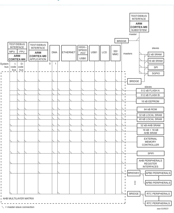
Fig 1. LPC43S6x Block diagram
ARM CORTEX-M4
TEST/DEBUG INTERFACE
I-code bus D-code bus system bus system bus
GPDMA LCD MMCSD/ ETHERNET 10/100 MAC IEEE 1588 HIGH-SPEED USB0 HOST/ DEVICE/OTG HIGH-SPEED USB1 HOST/DEVICE EMC HIGH-SPEED PHY CORE-CORE BRIDGE SPIFI HS GPIO SPI SGPIO SCTimer/PWM I2C0 I2S0 I2S1 C_CAN1 MOTOR CONTROL PWM TIMER3 TIMER2 USART2 USART3 SSP1 RI TIMER QEI GIMA
BRIDGE 0 BRIDGE 1 BRIDGE 2 BRIDGE 3 BRIDGE
MAIN AHB MULTILAYER MATRIX AHB MULTILAYER MATRIX
10-bit ADC0 10-bit ADC1 C_CAN0 I2C1 10-bit DAC BRIDGE RGU CCU2 CGU CCU1 ALARM TIMER CONFIGURATION REGISTERS OTP MEMORY EVENT ROUTER POWER MODE CONTROL
12 MHz IRC RTC POWER DOMAIN BACKUP REGISTERS RTC OSC RTC aaa-018919 slaves slaves masters masters ARM CORTEX-M0 APPLICATION TEST/DEBUG INTERFACE ARM CORTEX-M0 SUBSYSTEM TEST/DEBUG INTERFACE = connected to GPDMA GPIO INTERRUPTS GPIO GROUP0 INTERRUPT GPIO GROUP1 INTERRUPT WWDT USART0 UART1 SSP0 TIMER0 TIMER1 SCU 32 kB AHB SRAM 16 kB + 16 kB AHB SRAM 64 kB ROM 32 kB LOCAL SRAM 40 kB LOCAL SRAM slaves 2 kB LOCAL SRAM 16 kB LOCAL SRAM 512 kB FLASH A 512 kB FLASH B 16 kB EEPROM system bus AES ENCRYPTION/ DECRYPTION
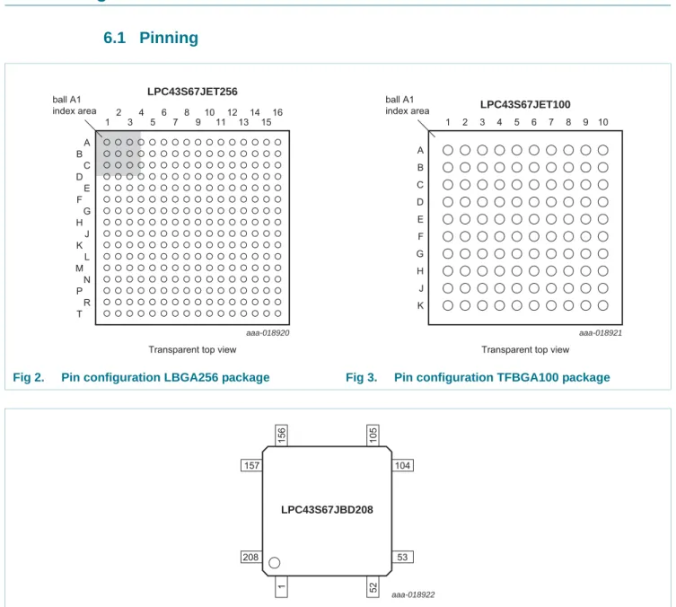
Fig 2. Pin configuration LBGA256 package Fig 3. Pin configuration TFBGA100 package
aaa-018920 LPC43S67JET256
Transparent top view T R P N M L J G K H F E D C B A 2 4 6 8 10 12 13 14 15 16 1 3 5 7 9 11 ball A1 index area aaa-018921 LPC43S67JET100
Transparent top view J G K H F E D C B A 2 4 6 8 10 1 3 5 7 9 ball A1 index area
Fig 4. Pin configuration LQFP208 package
LPC43S67JBD208 104 1 52 156 105 53 157 208 aaa-018922
assigned to it.
The parts contain two 10-bit ADCs (ADC0 and ADC1). The input channels of ADC0 and ADC1 on dedicated pins and multiplexed pins are combined in such a way that all channel 0 inputs (named ADC0_0 and ADC1_0) are tied together and connected to both, channel 0 on ADC0 and channel 0 on ADC1, channel 1 inputs (named ADC0_1 and ADC1_1) are tied together and connected to channel 1 on ADC0 and ADC1, and so forth. There are eight ADC channels total for the two ADCs.
Multiplexed digital pins
P0_0 L3 G2 47 [2] N;
PU
I/O GPIO0[0] — General purpose digital input/output pin. I/O SSP1_MISO — Master In Slave Out for SSP1.
I ENET_RXD1 — Ethernet receive data 1 (RMII/MII interface). I/O SGPIO0 — General purpose digital input/output pin.
- R — Function reserved.
- R — Function reserved.
I/O I2S0_TX_WS — Transmit Word Select. It is driven by the master and received by the slave. Corresponds to the signal WS in the I2S-bus specification.
I/O I2S1_TX_WS — Transmit Word Select. It is driven by the master and received by the slave. Corresponds to the signal WS in the I2S-bus specification.
P0_1 M2 G1 50 [2] N;
PU
I/O GPIO0[1] — General purpose digital input/output pin. I/O SSP1_MOSI — Master Out Slave in for SSP1.
I ENET_COL — Ethernet Collision detect (MII interface). I/O SGPIO1 — General purpose digital input/output pin.
- R — Function reserved.
- R — Function reserved.
ENET_TX_EN — Ethernet transmit enable (RMII/MII interface).
I/O I2S1_TX_SDA — I2S1 transmit data. It is driven by the transmitter and read by the receiver. Corresponds to the signal SD in the I2S-bus specification.
P1_0 P2 H1 54 [2] N;
PU
I/O GPIO0[4] — General purpose digital input/output pin. I CTIN_3 — SCT input 3. Capture input 1 of timer 1. I/O EMC_A5 — External memory address line 5.
- R — Function reserved.
- R — Function reserved.
I/O SSP0_SSEL — Slave Select for SSP0.
I/O SGPIO7 — General purpose digital input/output pin. I/O EMC_D12 — External memory data line 12.
P1_1 R2 K2 58 [2] N;
PU
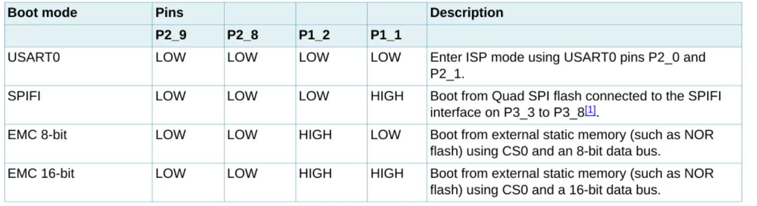
I/O GPIO0[8] — General purpose digital input/output pin. Boot pin (see Table 5).
O CTOUT_7 — SCT output 7. Match output 3 of timer 1. I/O EMC_A6 — External memory address line 6. I/O SGPIO8 — General purpose digital input/output pin.
- R — Function reserved.
I/O SSP0_MISO — Master In Slave Out for SSP0.
- R — Function reserved.
I/O EMC_D13 — External memory data line 13.
P1_2 R3 K1 60 [2] N;
PU
I/O GPIO0[9] — General purpose digital input/output pin. Boot pin (see Table 5).
O CTOUT_6 — SCT output 6. Match output 2 of timer 1. I/O EMC_A7 — External memory address line 7. I/O SGPIO9 — General purpose digital input/output pin.
- R — Function reserved.
I/O SSP0_MOSI — Master Out Slave in for SSP0.
- R — Function reserved.
I/O EMC_D14 — External memory data line 14.
P1_3 P5 J1 61 [2] N;
PU
I/O GPIO0[10] — General purpose digital input/output pin. O CTOUT_8 — SCT output 8. Match output 0 of timer 2. I/O SGPIO10 — General purpose digital input/output pin.
O EMC_OE — LOW active Output Enable signal.
O USB0_IND1 — USB0 port indicator LED control output 1.
I/O SSP1_MISO — Master In Slave Out for SSP1.
- R — Function reserved.
O SD_RST — SD/MMC reset signal for MMC4.4 card.
P1_4 T3 J2 64 [2] N;
PU
I/O GPIO0[11] — General purpose digital input/output pin. O CTOUT_9 — SCT output 9. Match output 3 of timer 3. I/O SGPIO11 — General purpose digital input/output pin. O EMC_BLS0 — LOW active Byte Lane select signal 0. O USB0_IND0 — USB0 port indicator LED control output 0. I/O SSP1_MOSI — Master Out Slave in for SSP1.
I/O EMC_D15 — External memory data line 15.
P1_5 R5 J4 65 [2] N;
PU
I/O GPIO1[8] — General purpose digital input/output pin. O CTOUT_10 — SCT output 10. Match output 3 of timer 3.
- R — Function reserved.
O EMC_CS0 — LOW active Chip Select 0 signal.
I USB0_PWR_FAULT — Port power fault signal indicating overcurrent condition; this signal monitors over-current on the USB bus (external circuitry required to detect over-current condition).
I/O SSP1_SSEL — Slave Select for SSP1.
I/O SGPIO15 — General purpose digital input/output pin.
O SD_POW — SD/MMC power monitor output.
P1_6 T4 K4 67 [2] N;
PU
I/O GPIO1[9] — General purpose digital input/output pin. I CTIN_5 — SCT input 5. Capture input 2 of timer 2.
- R — Function reserved.
O EMC_WE — LOW active Write Enable signal.
- R — Function reserved.
O EMC_BLS0 — LOW active Byte Lane select signal 0. I/O SGPIO14 — General purpose digital input/output pin.
I/O SD_CMD — SD/MMC command signal.
P1_7 T5 G4 69 [2] N;
PU
I/O GPIO1[0] — General purpose digital input/output pin.
I U1_DSR — Data Set Ready input for UART1.
O CTOUT_13 — SCT output 13. Match output 3 of timer 3. I/O EMC_D0 — External memory data line 0.
O USB0_PPWR — VBUS drive signal (towards external charge pump or power management unit); indicates that VBUS must be driven (active HIGH).
Add a pull-down resistor to disable the power switch at reset. This signal has opposite polarity compared to the USB_PPWR used on other NXP LPC parts.
- R — Function reserved.
- R — Function reserved.
P1_8 R7 H5 71 [2] N;
PU
I/O GPIO1[1] — General purpose digital input/output pin.
O U1_DTR — Data Terminal Ready output for UART1.
O CTOUT_12 — SCT output 12. Match output 3 of timer 3.
I/O EMC_D1 — External memory data line 1.
- R — Function reserved.
- R — Function reserved.
- R — Function reserved.
O SD_VOLT0 — SD/MMC bus voltage select output 0.
P1_9 T7 J5 73 [2] N;
PU
I/O GPIO1[2] — General purpose digital input/output pin.
O U1_RTS — Request to Send output for UART1.
O CTOUT_11 — SCT output 11. Match output 3 of timer 2. I/O EMC_D2 — External memory data line 2.
- R — Function reserved.
- R — Function reserved.
- R — Function reserved.
I/O SD_DAT0 — SD/MMC data bus line 0.
P1_10 R8 H6 75 [2] N;
PU
I/O GPIO1[3] — General purpose digital input/output pin. I U1_RI — Ring Indicator input for UART1.
O CTOUT_14 — SCT output 14. Match output 2 of timer 3. I/O EMC_D3 — External memory data line 3.
- R — Function reserved.
- R — Function reserved.
- R — Function reserved.
I/O SD_DAT1 — SD/MMC data bus line 1.
P1_11 T9 J7 77 [2] N;
PU
I/O GPIO1[4] — General purpose digital input/output pin. I U1_CTS — Clear to Send input for UART1.
O CTOUT_15 — SCT output 15. Match output 3 of timer 3. I/O EMC_D4 — External memory data line 4.
- R — Function reserved.
- R — Function reserved.
- R — Function reserved.
P1_12 R9 K7 78 [2] N;
PU
I/O GPIO1[5] — General purpose digital input/output pin. I U1_DCD — Data Carrier Detect input for UART1.
- R — Function reserved.
I/O EMC_D5 — External memory data line 5. I T0_CAP1 — Capture input 1 of timer 0.
- R — Function reserved.
I/O SGPIO8 — General purpose digital input/output pin. I/O SD_DAT3 — SD/MMC data bus line 3.
P1_13 R10 H8 83 [2] N;
PU
I/O GPIO1[6] — General purpose digital input/output pin. O U1_TXD — Transmitter output for UART1.
- R — Function reserved.
I/O EMC_D6 — External memory data line 6. I T0_CAP0 — Capture input 0 of timer 0.
- R — Function reserved.
I/O SGPIO9 — General purpose digital input/output pin.
I SD_CD — SD/MMC card detect input.
P1_14 R11 J8 85 [2] N;
PU
I/O GPIO1[7] — General purpose digital input/output pin.
I U1_RXD — Receiver input for UART1.
- R — Function reserved.
I/O EMC_D7 — External memory data line 7. O T0_MAT2 — Match output 2 of timer 0.
- R — Function reserved.
I/O SGPIO10 — General purpose digital input/output pin.
- R — Function reserved.
P1_15 T12 K8 87 [2] N;
PU
I/O GPIO0[2] — General purpose digital input/output pin.
O U2_TXD — Transmitter output for USART2.
I/O SGPIO2 — General purpose digital input/output pin.
I ENET_RXD0 — Ethernet receive data 0 (RMII/MII interface). O T0_MAT1 — Match output 1 of timer 0.
- R — Function reserved.
I/O EMC_D8 — External memory data line 8.
P1_16 M7 H9 90 [2] N;
PU
I/O GPIO0[3] — General purpose digital input/output pin.
I U2_RXD — Receiver input for USART2.
I/O SGPIO3 — General purpose digital input/output pin. I ENET_CRS — Ethernet Carrier Sense (MII interface). O T0_MAT0 — Match output 0 of timer 0.
- R — Function reserved.
I/O EMC_D9 — External memory data line 9.
I ENET_RX_DV — Ethernet Receive Data Valid (RMII/MII interface).
P1_17 M8 H10 93 [3] N;
PU
I/O GPIO0[12] — General purpose digital input/output pin. I/O U2_UCLK — Serial clock input/output for USART2 in
synchronous mode.
- R — Function reserved.
I/O ENET_MDIO — Ethernet MIIM data input and output. I T0_CAP3 — Capture input 3 of timer 0.
O CAN1_TD — CAN1 transmitter output.
I/O SGPIO11 — General purpose digital input/output pin.
- R — Function reserved.
P1_18 N12 J10 95 [2] N;
PU
I/O GPIO0[13] — General purpose digital input/output pin. I/O U2_DIR — RS-485/EIA-485 output enable/direction control for
USART2.
- R — Function reserved.
O ENET_TXD0 — Ethernet transmit data 0 (RMII/MII interface). O T0_MAT3 — Match output 3 of timer 0.
I CAN1_RD — CAN1 receiver input.
I/O SGPIO12 — General purpose digital input/output pin. I/O EMC_D10 — External memory data line 10.
P1_19 M11 K9 96 [2] N;
PU
I ENET_TX_CLK (ENET_REF_CLK) — Ethernet Transmit
Clock (MII interface) or Ethernet Reference Clock (RMII interface).
I/O SSP1_SCK — Serial clock for SSP1.
- R — Function reserved.
- R — Function reserved.
O CLKOUT — Clock output pin.
- R — Function reserved.
O I2S0_RX_MCLK — I2S receive master clock.
I/O I2S1_TX_SCK — Transmit Clock. It is driven by the master and received by the slave. Corresponds to the signal SCK in the I2S-bus specification.
P1_20 M10 K10 100 [2] N;
PU
I/O GPIO0[15] — General purpose digital input/output pin. I/O SSP1_SSEL — Slave Select for SSP1.
- R — Function reserved.
O ENET_TXD1 — Ethernet transmit data 1 (RMII/MII interface). I T0_CAP2 — Capture input 2 of timer 0.
- R — Function reserved.
I/O SGPIO13 — General purpose digital input/output pin. I/O EMC_D11 — External memory data line 11.
P2_0 T16 G10 108 [2] N;
PU
I/O SGPIO4 — General purpose digital input/output pin. O U0_TXD — Transmitter output for USART0. See Table 4 for
ISP mode.
I/O EMC_A13 — External memory address line 13.
O USB0_PPWR — VBUS drive signal (towards external charge pump or power management unit); indicates that VBUS must be driven (active HIGH).
Add a pull-down resistor to disable the power switch at reset. This signal has opposite polarity compared to the USB_PPWR used on other NXP LPC parts.
I/O GPIO5[0] — General purpose digital input/output pin.
- R — Function reserved.
I T3_CAP0 — Capture input 0 of timer 3.
O ENET_MDC — Ethernet MIIM clock.
P2_1 N15 G7 116 [2] N;
PU
I/O SGPIO5 — General purpose digital input/output pin.
I U0_RXD — Receiver input for USART0. See Table 4 for ISP mode.
I/O EMC_A12 — External memory address line 12.
I USB0_PWR_FAULT — Port power fault signal indicating overcurrent condition; this signal monitors over-current on the USB bus (external circuitry required to detect over-current condition).
I/O GPIO5[1] — General purpose digital input/output pin.
- R — Function reserved.
I T3_CAP1 — Capture input 1 of timer 3.
P2_2 M15 F5 121 [2] N;
PU
I/O SGPIO6 — General purpose digital input/output pin. I/O U0_UCLK — Serial clock input/output for USART0 in
synchronous mode.
I/O EMC_A11 — External memory address line 11.
O USB0_IND1 — USB0 port indicator LED control output 1. I/O GPIO5[2] — General purpose digital input/output pin. I CTIN_6 — SCT input 6. Capture input 1 of timer 3. I T3_CAP2 — Capture input 2 of timer 3.
O EMC_CS1 — LOW active Chip Select 1 signal.
P2_3 J12 D8 127 [3] N;
PU
I/O SGPIO12 — General purpose digital input/output pin. I/O I2C1_SDA — I2C1 data input/output (this pin does not use a
specialized I2C pad).
O U3_TXD — Transmitter output for USART3. See Table 4 for ISP mode.
I CTIN_1 — SCT input 1. Capture input 1 of timer 0. Capture input 1 of timer 2.
I/O GPIO5[3] — General purpose digital input/output pin.
- R — Function reserved.
O T3_MAT0 — Match output 0 of timer 3.
O USB0_PPWR — VBUS drive signal (towards external charge pump or power management unit); indicates that VBUS must be driven (active HIGH).
Add a pull-down resistor to disable the power switch at reset. This signal has opposite polarity compared to the USB_PPWR used on other NXP LPC parts.
P2_4 K11 D9 128 [3] N;
PU
I/O SGPIO13 — General purpose digital input/output pin. I/O I2C1_SCL — I2C1 clock input/output (this pin does not use a
specialized I2C pad).
I U3_RXD — Receiver input for USART3. See Table 4 for ISP mode.
I CTIN_0 — SCT input 0. Capture input 0 of timer 0, 1, 2, 3. I/O GPIO5[4] — General purpose digital input/output pin.
- R — Function reserved.
O T3_MAT1 — Match output 1 of timer 3.
I USB0_PWR_FAULT — Port power fault signal indicating overcurrent condition; this signal monitors over-current on the USB bus (external circuitry required to detect over-current condition).
P2_5 K14 D10 131 [3] N;
PU
I/O SGPIO14 — General purpose digital input/output pin. I CTIN_2 — SCT input 2. Capture input 2 of timer 0.
I USB1_VBUS — Monitors the presence of USB1 bus power.
Note: This signal must be HIGH for USB reset to occur.
I ADCTRIG1 — ADC trigger input 1.
I/O GPIO5[5] — General purpose digital input/output pin.
- R — Function reserved.
O T3_MAT2 — Match output 2 of timer 3.
O USB0_IND0 — USB0 port indicator LED control output 0.
P2_6 K16 G9 137 [2] N;
PU
I/O SGPIO7 — General purpose digital input/output pin.
I/O U0_DIR — RS-485/EIA-485 output enable/direction control for USART0.
I/O EMC_A10 — External memory address line 10. O USB0_IND0 — USB0 port indicator LED control
output 0.
I/O GPIO5[6] — General purpose digital input/output pin.
I CTIN_7 — SCT input 7.
I T3_CAP3 — Capture input 3 of timer 3.
O EMC_BLS1 — LOW active Byte Lane select signal 1.
P2_7 H14 C10 138 [2] N;
PU
I/O GPIO0[7] — General purpose digital input/output pin. If this pin is pulled LOW at reset, the part enters ISP mode or boots from an external source (see Table 4 and Table 5).
O CTOUT_1 — SCT output 1. Match output 3 of timer 3. I/O U3_UCLK — Serial clock input/output for USART3 in
synchronous mode.
I/O EMC_A9 — External memory address line 9.
- R — Function reserved.
- R — Function reserved.
O T3_MAT3 — Match output 3 of timer 3.
- R — Function reserved.
P2_8 J16 C6 140 [2] N;
PU
I/O SGPIO15 — General purpose digital input/output pin. Boot pin (see Table 5).
O CTOUT_0 — SCT output 0. Match output 0 of timer 0. I/O U3_DIR — RS-485/EIA-485 output enable/direction control for
USART3.
I/O EMC_A8 — External memory address line 8. I/O GPIO5[7] — General purpose digital input/output pin.
- R — Function reserved.
- R — Function reserved.
P2_9 H16 B10 144 [2] N;
PU
I/O GPIO1[10] — General purpose digital input/output pin. Boot pin (see Table 5).
O CTOUT_3 — SCT output 3. Match output 3 of timer 0.
I/O U3_BAUD — Baud pin for USART3.
I/O EMC_A0 — External memory address line 0.
- R — Function reserved. - R — Function reserved. - R — Function reserved. - R — Function reserved. P2_10 G16 E8 146 [2] N; PU
I/O GPIO0[14] — General purpose digital input/output pin. O CTOUT_2 — SCT output 2. Match output 2 of timer 0.
O U2_TXD — Transmitter output for USART2.
I/O EMC_A1 — External memory address line 1.
- R — Function reserved. - R — Function reserved. - R — Function reserved. - R — Function reserved. P2_11 F16 A9 148 [2] N; PU
I/O GPIO1[11] — General purpose digital input/output pin. O CTOUT_5 — SCT output 5. Match output 3 of timer 3.
I U2_RXD — Receiver input for USART2.
I/O EMC_A2 — External memory address line 2.
- R — Function reserved. - R — Function reserved. - R — Function reserved. - R — Function reserved. P2_12 E15 B9 153 [2] N; PU
I/O GPIO1[12] — General purpose digital input/output pin. O CTOUT_4 — SCT output 4. Match output 3 of timer 3.
- R — Function reserved.
I/O EMC_A3 — External memory address line 3.
- R — Function reserved.
- R — Function reserved.
- R — Function reserved.
I/O U2_UCLK — Serial clock input/output for USART2 in synchronous mode.
P2_13 C16 A10 156 [2] N;
PU
I/O GPIO1[13] — General purpose digital input/output pin. I CTIN_4 — SCT input 4. Capture input 2 of timer 1.
- R — Function reserved.
I/O EMC_A4 — External memory address line 4.
- R — Function reserved.
- R — Function reserved.
- R — Function reserved.
I/O U2_DIR — RS-485/EIA-485 output enable/direction control for USART2.
P3_0 F13 A8 161 [2] N;
PU
I/O I2S0_RX_SCK — I2S receive clock. It is driven by the master and received by the slave. Corresponds to the signal SCK in the I2S-bus specification.
O I2S0_RX_MCLK — I2S receive master clock.
I/O I2S0_TX_SCK — Transmit Clock. It is driven by the master and received by the slave. Corresponds to the signal SCK in the I2S-bus specification.
O I2S0_TX_MCLK — I2S transmit master clock.
I/O SSP0_SCK — Serial clock for SSP0.
- R — Function reserved.
- R — Function reserved.
- R — Function reserved.
P3_1 G11 F7 163 [2] N;
PU
I/O I2S0_TX_WS — Transmit Word Select. It is driven by the master and received by the slave. Corresponds to the signal WS in the I2S-bus specification.
I/O I2S0_RX_WS — Receive Word Select. It is driven by the master and received by the slave. Corresponds to the signal WS in the I2S-bus specification.
I CAN0_RD — CAN receiver input.
O USB1_IND1 — USB1 Port indicator LED control output 1. I/O GPIO5[8] — General purpose digital input/output pin.
- R — Function reserved.
O LCD_VD15 — LCD data.
P3_2 F11 G6 166 [2] OL;
PU
I/O I2S0_TX_SDA — I2S transmit data. It is driven by the transmitter and read by the receiver. Corresponds to the signal SD in the I2S-bus specification.
I/O I2S0_RX_SDA — I2S Receive data. It is driven by the transmitter and read by the receiver. Corresponds to the signal SD in the I2S-bus specification.
O CAN0_TD — CAN transmitter output.
O USB1_IND0 — USB1 Port indicator LED control output 0. I/O GPIO5[9] — General purpose digital input/output pin.
- R — Function reserved. O LCD_VD14 — LCD data. - R — Function reserved. P3_3 B14 A7 169 [4] N; PU - R — Function reserved.
I/O SPI_SCK — Serial clock for SPI. I/O SSP0_SCK — Serial clock for SSP0. O SPIFI_SCK — Serial clock for SPIFI.
O CGU_OUT1 — CGU spare clock output 1.
- R — Function reserved.
O I2S0_TX_MCLK — I2S transmit master clock.
I/O I2S1_TX_SCK — Transmit Clock. It is driven by the master and received by the slave. Corresponds to the signal SCK in the I2S-bus specification.
P3_4 A15 B8 171 [2] N;
PU
I/O GPIO1[14] — General purpose digital input/output pin.
- R — Function reserved.
- R — Function reserved.
I/O SPIFI_SIO3 — I/O lane 3 for SPIFI. O U1_TXD — Transmitter output for UART 1.
I/O I2S0_TX_WS — Transmit Word Select. It is driven by the master and received by the slave. Corresponds to the signal WS in the I2S-bus specification.
I/O I2S1_RX_SDA — I2S1 Receive data. It is driven by the transmitter and read by the receiver. Corresponds to the signal SD in the I2S-bus specification.
P3_5 C12 B7 173 [2] N;
PU
I/O GPIO1[15] — General purpose digital input/output pin.
- R — Function reserved.
- R — Function reserved.
I/O SPIFI_SIO2 — I/O lane 2 for SPIFI.
I U1_RXD — Receiver input for UART 1.
I/O I2S0_TX_SDA — I2S transmit data. It is driven by the transmitter and read by the receiver. Corresponds to the signal SD in the I2S-bus specification.
I/O I2S1_RX_WS — Receive Word Select. It is driven by the master and received by the slave. Corresponds to the signal WS in the I2S-bus specification.
O LCD_VD12 — LCD data.
P3_6 B13 C7 174 [2] N;
PU
I/O GPIO0[6] — General purpose digital input/output pin. I/O SPI_MISO — Master In Slave Out for SPI.
I/O SSP0_SSEL — Slave Select for SSP0.
I/O SPIFI_MISO — Input 1 in SPIFI quad mode; SPIFI output IO1.
- R — Function reserved.
I/O SSP0_MISO — Master In Slave Out for SSP0.
- R — Function reserved.
- R — Function reserved.
P3_7 C11 D7 176 [2] N;
PU
- R — Function reserved.
I/O SPI_MOSI — Master Out Slave In for SPI. I/O SSP0_MISO — Master In Slave Out for SSP0.
I/O SPIFI_MOSI — Input I0 in SPIFI quad mode; SPIFI output IO0.
I/O GPIO5[10] — General purpose digital input/output pin. I/O SSP0_MOSI — Master Out Slave in for SSP0.
- R — Function reserved.
- R — Function reserved.
P3_8 C10 E7 179 [2] N;
PU
- R — Function reserved.
I SPI_SSEL — Slave Select for SPI. Note that this pin in an input pin only. The SPI in master mode cannot drive the CS input on the slave. Any GPIO pin can be used for SPI chip select in master mode.
I/O SSP0_MOSI — Master Out Slave in for SSP0. I/O SPIFI_CS — SPIFI serial flash chip select.
I/O GPIO5[11] — General purpose digital input/output pin. I/O SSP0_SSEL — Slave Select for SSP0.
- R — Function reserved.
P4_0 D5 - 1 [2] N;
PU
I/O GPIO2[0] — General purpose digital input/output pin. O MCOA0 — Motor control PWM channel 0, output A. I NMI — External interrupt input to NMI.
- R — Function reserved.
- R — Function reserved.
O LCD_VD13 — LCD data.
I/O U3_UCLK — Serial clock input/output for USART3 in synchronous mode.
- R — Function reserved.
P4_1 A1 - 3 [5] N;
PU
I/O GPIO2[1] — General purpose digital input/output pin. O CTOUT_1 — SCT output 1. Match output 3 of timer 3.
O LCD_VD0 — LCD data.
- R — Function reserved.
- R — Function reserved.
O LCD_VD19 — LCD data.
O U3_TXD — Transmitter output for USART3.
I ENET_COL — Ethernet Collision detect (MII interface). AI ADC0_1 — ADC0 and ADC1, input channel 1. Configure the
pin as GPIO input and use the ADC function select register in the SCU to select the ADC.
P4_2 D3 - 12 [2] N;
PU
I/O GPIO2[2] — General purpose digital input/output pin. O CTOUT_0 — SCT output 0. Match output 0 of timer 0.
O LCD_VD3 — LCD data.
- R — Function reserved.
- R — Function reserved.
O LCD_VD12 — LCD data.
I U3_RXD — Receiver input for USART3.
I/O SGPIO8 — General purpose digital input/output pin.
P4_3 C2 - 10 [5] N;
PU
I/O GPIO2[3] — General purpose digital input/output pin. O CTOUT_3 — SCT output 3. Match output 3 of timer 0.
O LCD_VD2 — LCD data.
- R — Function reserved.
- R — Function reserved.
O LCD_VD21 — LCD data.
I/O U3_BAUD — Baud pin for USART3.
I/O SGPIO9 — General purpose digital input/output pin.
AI ADC0_0 — DAC, ADC0 and ADC1, input channel 0.
Configure the pin as GPIO input and use the ADC function select register in the SCU to select the ADC.
P4_4 B1 - 14 [5] N;
PU
I/O GPIO2[4] — General purpose digital input/output pin. O CTOUT_2 — SCT output 2. Match output 2 of timer 0.
O LCD_VD1 — LCD data.
- R — Function reserved.
- R — Function reserved.
O LCD_VD20 — LCD data.
I/O U3_DIR — RS-485/EIA-485 output enable/direction control for USART3.
I/O SGPIO10 — General purpose digital input/output pin.
O DAC — DAC output. Configure the pin as GPIO input and use the analog function select register in the SCU to select the DAC.
P4_5 D2 - 15 [2] N;
PU
I/O GPIO2[5] — General purpose digital input/output pin. O CTOUT_5 — SCT output 5. Match output 3 of timer 3. O LCD_FP — Frame pulse (STN). Vertical synchronization
pulse (TFT).
- R — Function reserved.
- R — Function reserved.
- R — Function reserved.
- R — Function reserved.
I/O SGPIO11 — General purpose digital input/output pin.
P4_6 C1 - 17 [2] N;
PU
I/O GPIO2[6] — General purpose digital input/output pin. O CTOUT_4 — SCT output 4. Match output 3 of timer 3.
O LCD_ENAB/LCDM — STN AC bias drive or TFT data enable
input.
- R — Function reserved.
- R — Function reserved.
- R — Function reserved.
- R — Function reserved.
P4_7 H4 - 21 [2] O;
PU
O LCD_DCLK — LCD panel clock.
I GP_CLKIN — General purpose clock input to the CGU.
- R — Function reserved.
- R — Function reserved.
- R — Function reserved.
- R — Function reserved.
I/O I2S1_TX_SCK — Transmit Clock. It is driven by the master and received by the slave. Corresponds to the signal SCK in the I2S-bus specification.
I/O I2S0_TX_SCK — Transmit Clock. It is driven by the master and received by the slave. Corresponds to the signal SCK in the I2S-bus specification.
P4_8 E2 - 23 [2] N;
PU
- R — Function reserved.
I CTIN_5 — SCT input 5. Capture input 2 of timer 2.
O LCD_VD9 — LCD data.
- R — Function reserved.
I/O GPIO5[12] — General purpose digital input/output pin.
O LCD_VD22 — LCD data.
O CAN1_TD — CAN1 transmitter output.
I/O SGPIO13 — General purpose digital input/output pin.
P4_9 L2 - 48 [2] N;
PU
- R — Function reserved.
I CTIN_6 — SCT input 6. Capture input 1 of timer 3.
O LCD_VD11 — LCD data.
- R — Function reserved.
I/O GPIO5[13] — General purpose digital input/output pin.
O LCD_VD15 — LCD data.
I CAN1_RD — CAN1 receiver input.
I/O SGPIO14 — General purpose digital input/output pin.
P4_10 M3 - 51 [2] N;
PU
- R — Function reserved.
I CTIN_2 — SCT input 2. Capture input 2 of timer 0.
O LCD_VD10 — LCD data.
- R — Function reserved.
I/O GPIO5[14] — General purpose digital input/output pin.
O LCD_VD14 — LCD data.
- R — Function reserved.
P5_0 N3 - 53 [2] N;
PU
I/O GPIO2[9] — General purpose digital input/output pin. O MCOB2 — Motor control PWM channel 2, output B. I/O EMC_D12 — External memory data line 12.
- R — Function reserved.
I U1_DSR — Data Set Ready input for UART 1.
I T1_CAP0 — Capture input 0 of timer 1.
- R — Function reserved.
- R — Function reserved.
P5_1 P3 - 55 [2] N;
PU
I/O GPIO2[10] — General purpose digital input/output pin. I MCI2 — Motor control PWM channel 2, input.
I/O EMC_D13 — External memory data line 13.
- R — Function reserved.
O U1_DTR — Data Terminal Ready output for UART 1. Can also be configured to be an RS-485/EIA-485 output enable signal for UART 1.
I T1_CAP1 — Capture input 1 of timer 1.
- R — Function reserved.
- R — Function reserved.
P5_2 R4 - 63 [2] N;
PU
I/O GPIO2[11] — General purpose digital input/output pin. I MCI1 — Motor control PWM channel 1, input.
I/O EMC_D14 — External memory data line 14.
- R — Function reserved.
O U1_RTS — Request to Send output for UART 1. Can also be configured to be an RS-485/EIA-485 output enable signal for UART 1.
I T1_CAP2 — Capture input 2 of timer 1.
- R — Function reserved.
- R — Function reserved.
P5_3 T8 - 76 [2] N;
PU
I/O GPIO2[12] — General purpose digital input/output pin. I MCI0 — Motor control PWM channel 0, input.
I/O EMC_D15 — External memory data line 15.
- R — Function reserved.
I U1_RI — Ring Indicator input for UART 1. I T1_CAP3 — Capture input 3 of timer 1.
- R — Function reserved.
P5_4 P9 - 80 [2] N;
PU
I/O GPIO2[13] — General purpose digital input/output pin. O MCOB0 — Motor control PWM channel 0, output B. I/O EMC_D8 — External memory data line 8.
- R — Function reserved.
I U1_CTS — Clear to Send input for UART 1. O T1_MAT0 — Match output 0 of timer 1.
- R — Function reserved.
- R — Function reserved.
P5_5 P10 - 81 [2] N;
PU
I/O GPIO2[14] — General purpose digital input/output pin. O MCOA1 — Motor control PWM channel 1, output A. I/O EMC_D9 — External memory data line 9.
- R — Function reserved.
I U1_DCD — Data Carrier Detect input for UART 1. O T1_MAT1 — Match output 1 of timer 1.
- R — Function reserved.
- R — Function reserved.
P5_6 T13 - 89 [2] N;
PU
I/O GPIO2[15] — General purpose digital input/output pin. O MCOB1 — Motor control PWM channel 1, output B. I/O EMC_D10 — External memory data line 10.
- R — Function reserved.
O U1_TXD — Transmitter output for UART 1. O T1_MAT2 — Match output 2 of timer 1.
- R — Function reserved.
- R — Function reserved.
P5_7 R12 - 91 [2] N;
PU
I/O GPIO2[7] — General purpose digital input/output pin. O MCOA2 — Motor control PWM channel 2, output A. I/O EMC_D11 — External memory data line 11.
- R — Function reserved.
I U1_RXD — Receiver input for UART 1.
O T1_MAT3 — Match output 3 of timer 1.
- R — Function reserved.
P6_0 M12 H7 105 [2] N;
PU
- R — Function reserved.
O I2S0_RX_MCLK — I2S receive master clock.
- R — Function reserved.
- R — Function reserved.
I/O I2S0_RX_SCK — Receive Clock. It is driven by the master and received by the slave. Corresponds to the signal SCK in the I2S-bus specification.
- R — Function reserved.
- R — Function reserved.
- R — Function reserved.
P6_1 R15 G5 107 [2] N;
PU
I/O GPIO3[0] — General purpose digital input/output pin.
O EMC_DYCS1 — SDRAM chip select 1.
I/O U0_UCLK — Serial clock input/output for USART0 in synchronous mode.
I/O I2S0_RX_WS — Receive Word Select. It is driven by the master and received by the slave. Corresponds to the signal WS in the I2S-bus specification.
- R — Function reserved.
I T2_CAP0 — Capture input 2 of timer 2.
- R — Function reserved.
- R — Function reserved.
P6_2 L13 J9 111 [2] N;
PU
I/O GPIO3[1] — General purpose digital input/output pin.
O EMC_CKEOUT1 — SDRAM clock enable 1.
I/O U0_DIR — RS-485/EIA-485 output enable/direction control for USART0.
I/O I2S0_RX_SDA — I2S Receive data. It is driven by the transmitter and read by the receiver. Corresponds to the signal SD in the I2S-bus specification.
- R — Function reserved.
I T2_CAP1 — Capture input 1 of timer 2.
- R — Function reserved.
P6_3 P15 - 113 [2] N;
PU
I/O GPIO3[2] — General purpose digital input/output pin.
O USB0_PPWR — VBUS drive signal (towards external charge pump or power management unit); indicates that the VBUS signal must be driven (active HIGH).
Add a pull-down resistor to disable the power switch at reset. This signal has opposite polarity compared to the USB_PPWR used on other NXP LPC parts.
I/O SGPIO4 — General purpose digital input/output pin. O EMC_CS1 — LOW active Chip Select 1 signal.
- R — Function reserved.
I T2_CAP2 — Capture input 2 of timer 2.
- R — Function reserved.
- R — Function reserved.
P6_4 R16 F6 114 [2] N;
PU
I/O GPIO3[3] — General purpose digital input/output pin. I CTIN_6 — SCT input 6. Capture input 1 of timer 3.
O U0_TXD — Transmitter output for USART0.
O EMC_CAS — LOW active SDRAM Column Address Strobe.
- R — Function reserved. - R — Function reserved. - R — Function reserved. - R — Function reserved. P6_5 P16 F9 117 [2] N; PU
I/O GPIO3[4] — General purpose digital input/output pin. O CTOUT_6 — SCT output 6. Match output 2 of timer 1.
I U0_RXD — Receiver input for USART0.
O EMC_RAS — LOW active SDRAM Row Address Strobe.
- R — Function reserved. - R — Function reserved. - R — Function reserved. - R — Function reserved. P6_6 L14 - 119 [2] N; PU
I/O GPIO0[5] — General purpose digital input/output pin. O EMC_BLS1 — LOW active Byte Lane select signal 1. I/O SGPIO5 — General purpose digital input/output pin. I USB0_PWR_FAULT — Port power fault signal indicating
overcurrent condition; this signal monitors over-current on the USB bus (external circuitry required to detect over-current condition).
- R — Function reserved.
I T2_CAP3 — Capture input 3 of timer 2.
- R — Function reserved.
P6_7 J13 - 123 [2] N;
PU
- R — Function reserved.
I/O EMC_A15 — External memory address line 15. I/O SGPIO6 — General purpose digital input/output pin. O USB0_IND1 — USB0 port indicator LED control output 1. I/O GPIO5[15] — General purpose digital input/output pin. O T2_MAT0 — Match output 0 of timer 2.
- R — Function reserved.
- R — Function reserved.
P6_8 H13 - 125 [2] N;
PU
- R — Function reserved.
I/O EMC_A14 — External memory address line 14. I/O SGPIO7 — General purpose digital input/output pin. O USB0_IND0 — USB0 port indicator LED control output 0. I/O GPIO5[16] — General purpose digital input/output pin. O T2_MAT1 — Match output 1 of timer 2.
- R — Function reserved.
- R — Function reserved.
P6_9 J15 F8 139 [2] N;
PU
I/O GPIO3[5] — General purpose digital input/output pin.
- R — Function reserved.
- R — Function reserved.
O EMC_DYCS0 — SDRAM chip select 0.
- R — Function reserved.
O T2_MAT2 — Match output 2 of timer 2.
- R — Function reserved.
- R — Function reserved.
P6_10 H15 - 142 [2] N;
PU
I/O GPIO3[6] — General purpose digital input/output pin.
O MCABORT — Motor control PWM, LOW-active fast abort.
- R — Function reserved.
O EMC_DQMOUT1 — Data mask 1 used with SDRAM and
static devices.
- R — Function reserved.
- R — Function reserved.
- R — Function reserved.
P6_11 H12 C9 143 [2] N;
PU
I/O GPIO3[7] — General purpose digital input/output pin.
- R — Function reserved.
- R — Function reserved.
O EMC_CKEOUT0 — SDRAM clock enable 0.
- R — Function reserved.
O T2_MAT3 — Match output 3 of timer 2.
- R — Function reserved.
- R — Function reserved.
P6_12 G15 - 145 [2] N;
PU
I/O GPIO2[8] — General purpose digital input/output pin. O CTOUT_7 — SCT output 7. Match output 3 of timer 1.
- R — Function reserved.
O EMC_DQMOUT0 — Data mask 0 used with SDRAM and
static devices. - R — Function reserved. - R — Function reserved. - R — Function reserved. - R — Function reserved. P7_0 B16 - 158 [2] N; PU
I/O GPIO3[8] — General purpose digital input/output pin. O CTOUT_14 — SCT output 14. Match output 2 of timer 3.
- R — Function reserved.
O LCD_LE — Line end signal.
- R — Function reserved.
- R — Function reserved.
- R — Function reserved.
I/O SGPIO4 — General purpose digital input/output pin.
P7_1 C14 - 162 [2] N;
PU
I/O GPIO3[9] — General purpose digital input/output pin. O CTOUT_15 — SCT output 15. Match output 3 of timer 3. I/O I2S0_TX_WS — Transmit Word Select. It is driven by the
master and received by the slave. Corresponds to the signal WS in the I2S-bus specification.
O LCD_VD19 — LCD data.
O LCD_VD7 — LCD data.
- R — Function reserved.
O U2_TXD — Transmitter output for USART2.
P7_2 A16 - 165 [2] N;
PU
I/O GPIO3[10] — General purpose digital input/output pin. I CTIN_4 — SCT input 4. Capture input 2 of timer 1. I/O I2S0_TX_SDA — I2S transmit data. It is driven by the
transmitter and read by the receiver. Corresponds to the signal SD in the I2S-bus specification.
O LCD_VD18 — LCD data.
O LCD_VD6 — LCD data.
- R — Function reserved.
I U2_RXD — Receiver input for USART2.
I/O SGPIO6 — General purpose digital input/output pin.
P7_3 C13 - 167 [2] N;
PU
I/O GPIO3[11] — General purpose digital input/output pin. I CTIN_3 — SCT input 3. Capture input 1 of timer 1.
- R — Function reserved. O LCD_VD17 — LCD data. O LCD_VD5 — LCD data. - R — Function reserved. - R — Function reserved. - R — Function reserved. P7_4 C8 - 189 [5] N; PU
I/O GPIO3[12] — General purpose digital input/output pin. O CTOUT_13 — SCT output 13. Match output 3 of timer 3.
- R — Function reserved.
O LCD_VD16 — LCD data.
O LCD_VD4 — LCD data.
O TRACEDATA[0] — Trace data, bit 0.
- R — Function reserved.
- R — Function reserved.
AI ADC0_4 — ADC0 and ADC1, input channel 4. Configure the pin as GPIO input and use the ADC function select register in the SCU to select the ADC.
P7_5 A7 - 191 [5] N;
PU
I/O GPIO3[13] — General purpose digital input/output pin. O CTOUT_12 — SCT output 12. Match output 3 of timer 3.
- R — Function reserved.
O LCD_VD8 — LCD data.
O LCD_VD23 — LCD data.
O TRACEDATA[1] — Trace data, bit 1.
- R — Function reserved.
- R — Function reserved.
AI ADC0_3 — ADC0 and ADC1, input channel 3. Configure the pin as GPIO input and use the ADC function select register in the SCU to select the ADC.
P7_6 C7 - 194 [2] N;
PU
I/O GPIO3[14] — General purpose digital input/output pin. O CTOUT_11 — SCT output 1. Match output 3 of timer 2.
- R — Function reserved.
O LCD_LP — Line synchronization pulse (STN). Horizontal synchronization pulse (TFT).
- R — Function reserved.
O TRACEDATA[2] — Trace data, bit 2.
- R — Function reserved.
- R — Function reserved.
P7_7 B6 - 201 [5] N;
PU
I/O GPIO3[15] — General purpose digital input/output pin. O CTOUT_8 — SCT output 8. Match output 0 of timer 2.
- R — Function reserved.
O LCD_PWR — LCD panel power enable.
- R — Function reserved.
O TRACEDATA[3] — Trace data, bit 3.
O ENET_MDC — Ethernet MIIM clock.
I/O SGPIO7 — General purpose digital input/output pin.
AI ADC1_6 — ADC1 and ADC0, input channel 6. Configure the pin as GPIO input and use the ADC function select register in the SCU to select the ADC.
P8_0 E5 - 2 [3] N;
PU
I/O GPIO4[0] — General purpose digital input/output pin. I USB0_PWR_FAULT — Port power fault signal indicating
overcurrent condition; this signal monitors over-current on the USB bus (external circuitry required to detect over-current condition).
- R — Function reserved.
I MCI2 — Motor control PWM channel 2, input. I/O SGPIO8 — General purpose digital input/output pin.
- R — Function reserved.
- R — Function reserved.
O T0_MAT0 — Match output 0 of timer 0.
P8_1 H5 - 34 [3] N;
PU
I/O GPIO4[1] — General purpose digital input/output pin. O USB0_IND1 — USB0 port indicator LED control output 1.
- R — Function reserved.
I MCI1 — Motor control PWM channel 1, input. I/O SGPIO9 — General purpose digital input/output pin.
- R — Function reserved.
- R — Function reserved.
P8_2 K4 - 36 [3] N;
PU
I/O GPIO4[2] — General purpose digital input/output pin. O USB0_IND0 — USB0 port indicator LED control output 0.
- R — Function reserved.
I MCI0 — Motor control PWM channel 0, input. I/O SGPIO10 — General purpose digital input/output pin.
- R — Function reserved.
- R — Function reserved.
O T0_MAT2 — Match output 2 of timer 0.
P8_3 J3 - 37 [2] N;
PU
I/O GPIO4[3] — General purpose digital input/output pin. I/O USB1_ULPI_D2 — ULPI link bidirectional data line 2.
- R — Function reserved.
O LCD_VD12 — LCD data.
O LCD_VD19 — LCD data.
- R — Function reserved.
- R — Function reserved.
O T0_MAT3 — Match output 3 of timer 0.
P8_4 J2 - 39 [2] N;
PU
I/O GPIO4[4] — General purpose digital input/output pin. I/O USB1_ULPI_D1 — ULPI link bidirectional data line 1.
- R — Function reserved.
O LCD_VD7 — LCD data.
O LCD_VD16 — LCD data.
- R — Function reserved.
- R — Function reserved.
I T0_CAP0 — Capture input 0 of timer 0.
P8_5 J1 - 40 [2] N;
PU
I/O GPIO4[5] — General purpose digital input/output pin. I/O USB1_ULPI_D0 — ULPI link bidirectional data line 0.
- R — Function reserved.
O LCD_VD6 — LCD data.
O LCD_VD8 — LCD data.
- R — Function reserved.
- R — Function reserved.
P8_6 K3 - 43 [2] N;
PU
I/O GPIO4[6] — General purpose digital input/output pin. I USB1_ULPI_NXT — ULPI link NXT signal. Data flow control
signal from the PHY.
- R — Function reserved.
O LCD_VD5 — LCD data.
O LCD_LP — Line synchronization pulse (STN). Horizontal synchronization pulse (TFT).
- R — Function reserved.
- R — Function reserved.
I T0_CAP2 — Capture input 2 of timer 0.
P8_7 K1 - 45 [2] N;
PU
I/O GPIO4[7] — General purpose digital input/output pin.
O USB1_ULPI_STP — ULPI link STP signal. Asserted to end or interrupt transfers to the PHY.
- R — Function reserved.
O LCD_VD4 — LCD data.
O LCD_PWR — LCD panel power enable.
- R — Function reserved.
- R — Function reserved.
I T0_CAP3 — Capture input 3 of timer 0.
P8_8 L1 - 49 [2] N;
PU
- R — Function reserved.
I USB1_ULPI_CLK — ULPI link CLK signal. 60 MHz clock
generated by the PHY.
- R — Function reserved.
- R — Function reserved.
- R — Function reserved.
- R — Function reserved.
O CGU_OUT0 — CGU spare clock output 0.
O I2S1_TX_MCLK — I2S1 transmit master clock.
P9_0 T1 - 59 [2] N;
PU
I/O GPIO4[12] — General purpose digital input/output pin.
O MCABORT — Motor control PWM, LOW-active fast abort.
- R — Function reserved.
- R — Function reserved.
- R — Function reserved.
I ENET_CRS — Ethernet Carrier Sense (MII interface). I/O SGPIO0 — General purpose digital input/output pin. I/O SSP0_SSEL — Slave Select for SSP0.
P9_1 N6 - 66 [2] N;
PU
I/O GPIO4[13] — General purpose digital input/output pin. O MCOA2 — Motor control PWM channel 2, output A.
- R — Function reserved.
- R — Function reserved.
I/O I2S0_TX_WS — Transmit Word Select. It is driven by the master and received by the slave. Corresponds to the signal WS in the I2S-bus specification.
I ENET_RX_ER — Ethernet receive error (MII interface). I/O SGPIO1 — General purpose digital input/output pin. I/O SSP0_MISO — Master In Slave Out for SSP0.
P9_2 N8 - 70 [2] N;
PU
I/O GPIO4[14] — General purpose digital input/output pin. O MCOB2 — Motor control PWM channel 2, output B.
- R — Function reserved.
- R — Function reserved.
I/O I2S0_TX_SDA — I2S transmit data. It is driven by the transmitter and read by the receiver. Corresponds to the signal SD in the I2S-bus specification.
I ENET_RXD3 — Ethernet receive data 3 (MII interface). I/O SGPIO2 — General purpose digital input/output pin. I/O SSP0_MOSI — Master Out Slave in for SSP0.
P9_3 M6 - 79 [2] N;
PU
I/O GPIO4[15] — General purpose digital input/output pin. O MCOA0 — Motor control PWM channel 0, output A. O USB1_IND1 — USB1 Port indicator LED control output 1.
- R — Function reserved.
- R — Function reserved.
I ENET_RXD2 — Ethernet receive data 2 (MII interface). I/O SGPIO9 — General purpose digital input/output pin.
O U3_TXD — Transmitter output for USART3.
P9_4 N10 - 92 [2] N;
PU
- R — Function reserved.
O MCOB0 — Motor control PWM channel 0, output B. O USB1_IND0 — USB1 Port indicator LED control output 0.
- R — Function reserved.
I/O GPIO5[17] — General purpose digital input/output pin. O ENET_TXD2 — Ethernet transmit data 2 (MII interface). I/O SGPIO4 — General purpose digital input/output pin.
P9_5 M9 - 98 [2] N;
PU
- R — Function reserved.
O MCOA1 — Motor control PWM channel 1, output A.
O USB1_PPWR — VBUS drive signal (towards external charge pump or power management unit); indicates that VBUS must be driven (active high).
Add a pull-down resistor to disable the power switch at reset. This signal has opposite polarity compared to the USB_PPWR used on other NXP LPC parts.
- R — Function reserved.
I/O GPIO5[18] — General purpose digital input/output pin. O ENET_TXD3 — Ethernet transmit data 3 (MII interface). I/O SGPIO3 — General purpose digital input/output pin.
O U0_TXD — Transmitter output for USART0.
P9_6 L11 - 103 [2] N;
PU
I/O GPIO4[11] — General purpose digital input/output pin. O MCOB1 — Motor control PWM channel 1, output B.
I USB1_PWR_FAULT — USB1 Port power fault signal
indicating over-current condition; this signal monitors over-current on the USB1 bus (external circuitry required to detect over-current condition).
- R — Function reserved.
- R — Function reserved.
I ENET_COL — Ethernet Collision detect (MII interface). I/O SGPIO8 — General purpose digital input/output pin.
I U0_RXD — Receiver input for USART0.
PA_0 L12 - 126 [2] N; PU - R — Function reserved. - R — Function reserved. - R — Function reserved. - R — Function reserved. - R — Function reserved.
O I2S1_RX_MCLK — I2S1 receive master clock.
O CGU_OUT1 — CGU spare clock output 1.
- R — Function reserved.
PA_1 J14 - 134 [3] N;
PU
I/O GPIO4[8] — General purpose digital input/output pin. I QEI_IDX — Quadrature Encoder Interface INDEX input.
- R — Function reserved.
O U2_TXD — Transmitter output for USART2.
- R — Function reserved.
- R — Function reserved.
- R — Function reserved.
PA_2 K15 - 136 [3] N;
PU
I/O GPIO4[9] — General purpose digital input/output pin. I QEI_PHB — Quadrature Encoder Interface PHB input.
- R — Function reserved.
I U2_RXD — Receiver input for USART2.
- R — Function reserved. - R — Function reserved. - R — Function reserved. - R — Function reserved. PA_3 H11 - 147 [3] N; PU
I/O GPIO4[10] — General purpose digital input/output pin. I QEI_PHA — Quadrature Encoder Interface PHA input.
- R — Function reserved. - R — Function reserved. - R — Function reserved. - R — Function reserved. - R — Function reserved. - R — Function reserved. PA_4 G13 - 151 [2] N; PU - R — Function reserved.
O CTOUT_9 — SCT output 9. Match output 3 of timer 3.
- R — Function reserved.
I/O EMC_A23 — External memory address line 23. I/O GPIO5[19] — General purpose digital input/output pin.
- R — Function reserved. - R — Function reserved. - R — Function reserved. PB_0 B15 - 164 [2] N; PU - R — Function reserved.
O CTOUT_10 — SCT output 10. Match output 3 of timer 3.
O LCD_VD23 — LCD data.
- R — Function reserved.
I/O GPIO5[20] — General purpose digital input/output pin.
- R — Function reserved.
- R — Function reserved.
PB_1 A14 - 175 [2] N;
PU
- R — Function reserved.
I USB1_ULPI_DIR — ULPI link DIR signal. Controls the ULP data line direction.
O LCD_VD22 — LCD data.
- R — Function reserved.
I/O GPIO5[21] — General purpose digital input/output pin. O CTOUT_6 — SCT output 6. Match output 2 of timer 1.
- R — Function reserved.
- R — Function reserved.
PB_2 B12 - 177 [2] N;
PU
- R — Function reserved.
I/O USB1_ULPI_D7 — ULPI link bidirectional data line 7.
O LCD_VD21 — LCD data.
- R — Function reserved.
I/O GPIO5[22] — General purpose digital input/output pin. O CTOUT_7 — SCT output 7. Match output 3 of timer 1.
- R — Function reserved.
- R — Function reserved.
PB_3 A13 - 178 [2] N;
PU
- R — Function reserved.
I/O USB1_ULPI_D6 — ULPI link bidirectional data line 6.
O LCD_VD20 — LCD data.
- R — Function reserved.
I/O GPIO5[23] — General purpose digital input/output pin. O CTOUT_8 — SCT output 8. Match output 0 of timer 2.
- R — Function reserved.
- R — Function reserved.
PB_4 B11 - 180 [2] N;
PU
- R — Function reserved.
I/O USB1_ULPI_D5 — ULPI link bidirectional data line 5.
O LCD_VD15 — LCD data.
- R — Function reserved.
I/O GPIO5[24] — General purpose digital input/output pin. I CTIN_5 — SCT input 5. Capture input 2 of timer 2.
- R — Function reserved.
PB_5 A12 - 181 [2] N;
PU
- R — Function reserved.
I/O USB1_ULPI_D4 — ULPI link bidirectional data line 4.
O LCD_VD14 — LCD data.
- R — Function reserved.
I/O GPIO5[25] — General purpose digital input/output pin.
I CTIN_7 — SCT input 7.
O LCD_PWR — LCD panel power enable.
- R — Function reserved.
PB_6 A6 - - [5] N;
PU
- R — Function reserved.
I/O USB1_ULPI_D3 — ULPI link bidirectional data line 3.
O LCD_VD13 — LCD data.
- R — Function reserved.
I/O GPIO5[26] — General purpose digital input/output pin. I CTIN_6 — SCT input 6. Capture input 1 of timer 3.
O LCD_VD19 — LCD data.
- R — Function reserved.
AI ADC0_6 — ADC0 and ADC1, input channel 6. Configure the pin as GPIO input and use the ADC function select register in the SCU to select the ADC.
PC_0 D4 - 7 [5] N;
PU
- R — Function reserved.
I USB1_ULPI_CLK — ULPI link CLK signal. 60 MHz clock
generated by the PHY.
- R — Function reserved.
I/O ENET_RX_CLK — Ethernet Receive Clock (MII interface).
O LCD_DCLK — LCD panel clock.
- R — Function reserved.
- R — Function reserved.
I/O SD_CLK — SD/MMC card clock.
AI ADC1_1 — ADC1 and ADC0, input channel 1. Configure the pin as input (USB_ULPI_CLK) and use the ADC function select register in the SCU to select the ADC.
PC_1 E4 - 9 [2] N;
PU
I/O USB1_ULPI_D7 — ULPI link bidirectional data line 7.
- R — Function reserved.
I U1_RI — Ring Indicator input for UART 1.
O ENET_MDC — Ethernet MIIM clock.
I/O GPIO6[0] — General purpose digital input/output pin.
- R — Function reserved.
I T3_CAP0 — Capture input 0 of timer 3.