U
NIVERSITY OFN
ORTHC
AROLINA ATC
HAPELH
ILL DEPARTMENT OR COMPUTERSCIENCESENIORHONORSTHESIS
A frameless image sensor with application in
astronomy
By
Yi HU
Advisor:
Montek S
INGHSecond Reader:
Ketan M
AYER-P
ATELAbstract
ii
Acknowledgements
iii
Contents
Abstract i
Acknowledgements ii
1 Introduction 1
1.1 Motivation and Research Objectives . . . 1
1.1.1 Motivation . . . 1
1.1.2 Research Objectives . . . 1
1.2 Domain Requirements . . . 2
1.2.1 General Purpose Photography . . . 2
1.2.2 Astronomy . . . 2
1.3 Organization of the Thesis . . . 3
2 Background: Sensors 4 2.1 Introduction: Conventional CCD and CMOS Sensors . . . 4
2.2 Performance Metrics for Image Sensors . . . 4
2.2.1 Signal-to-Noise Ratio (SNR) . . . 6
2.2.2 Dynamic Range (DR) . . . 6
2.2.3 Frame Rate . . . 7
2.2.4 Dark Current . . . 7
2.2.5 Fill Factor (FF) . . . 7
2.2.6 Quantum Efficiency (QE) . . . 8
2.2.7 Cost and Power Consumption . . . 8
2.3 Physics of Photodetectors . . . 8
2.3.1 Photodiodes . . . 9
Accumulation Mode . . . 11
P-i-N Photodiodes . . . 11
2.3.2 Pinned Photodiodes (PPD) . . . 12
2.3.3 Single-Photon Avalanche Diodes (SPADs) . . . 14
SPAD Specific Performance Metrics . . . 15
2.3.4 Photogates (MOS Capacitors) . . . 15
2.4 Conventional Sensor Technologies Revisited . . . 15
2.4.1 CCD Image Sensors . . . 15
Pros and Cons . . . 17
2.4.2 CMOS Image Sensors . . . 17
Pros and Cons . . . 17
2.4.3 Dynamic range: fixed frame time . . . 18
iv
3 Background: Frameless Image Sensor 20
3.1 Design . . . 20
3.2 Advantages . . . 22
4 Improvement 1: Low-Light Detection via Noise Reduction 23 4.1 Challenge: Noise . . . 23
4.1.1 kTC Reset Noise . . . 23
4.2 Approaches to Mitigate Reset Noise . . . 23
4.2.1 Noise subtraction via two-threshold sampling . . . 23
4.2.2 Noise averaging via repeated sampling . . . 25
4.2.3 Combined approach . . . 27
4.3 Summary . . . 28
5 Improvement 2: Single Photon Detection 29 5.1 Single-Photon Avalanche Diode (SPAD) Implementation . . . 29
5.1.1 Circuit Design . . . 29
5.1.2 Challenges . . . 31
6 Summary and Conclusion 32 6.1 Comparison . . . 32
6.2 Future work . . . 33
v
List of Figures
2.1 Simplified frame-transfer(FT) CCD architecture. (Source: [4]) . 5
2.2 Simplified CMOS architecture. (Source: [11]) . . . 5
2.3 Electron-hole generation by excitation with photons of energy Eph >Eg. (Source: [11]) . . . 9
2.4 Absorption spectrum (Source: [11]) . . . 9
2.5 Ideal PN junction properties. (Source: [13] ) . . . 10
2.6 Photogeneration in a PN junction. (Source: [13] ) . . . 10
2.7 Abstract circuit for accumulation mode operation. (Source: [13]) 11 2.8 Ideal P-i-N junction properties. (Source: [13] ) . . . 12
2.9 Cross-section of PPD. . . 13
2.10 PPD pixel. (Source: [1]) . . . 13
2.11 PPD basic operation. (Source: [1]) . . . 13
2.12 SPAD structure. (Source: [13] ) . . . 14
2.13 SPAD operation cycle. . . 14
2.14 Photogate structure. (Source: [8]) . . . 15
2.15 Charge transfer between gates. . . 16
2.16 Charge transfer in 3-phase CCD. (Source: [12]) . . . 16
2.17 Active Pixel Sensor (APS) . . . 18
3.1 Frameless pixel architecture (Follow [10]) . . . 20
3.2 Frameless pixel circuit implementation . . . 21
3.3 ExampleVD andVoutwaveform. . . 21
4.1 Circuit implementation of the two-threshold sampling. . . 24
4.2 ExampleVD andVoutwaveforms with two-threshold sampling 24 4.3 Circuit implementation of a pulse generator. . . 25
4.4 Circuit implementation of the repeated sampling. . . 26
4.5 ExampleVD and Vout waveforms before/after applying two-threshold sampling. (Upper: before. Lower: after) . . . 26
4.6 Simple current mirror circuit. . . 27
4.7 Circuit implementation of the combined approach. . . 27
vi
List of Tables
2.1 Summary of CCD and CMOS image sensors. . . 19
6.1 Comparison among CCD, CMOS, frameless, frameless with noise reduction, and frameless with single photon detection image sensors. . . 33
List of Symbols
D dark current A/pixel (electrons/pixel/s)
T temperature K
t time s
Nr read noise per pixel electrons rms/pixel
P incident photon flux per pixel photons/pixel/s
B background photon flux per pixel photons/pixel/s
Qe quantum efficiency %
R surface reflectance %
Nsat full well capacity per pixel electrons/pixel
Eph photon energy J
Eg bandgap J
EC conduction band energy J
EV valence band energy J
ν photon frequency s−1
Iph photocurrent A
tint integration time s
V0 built-in potential of diodes V
VBD breakdown voltage of the SPAD V
VEX excessive voltage of the SPAD V
vg gate voltage V
λ wavelength m
vii
List of Abbreviations
CCD Charge-CoupledDevice
CMOS ComplementaryMetal-Oxide-Semicondector
MOS Metal-Oxide-Semicondector
SPAD Single-PhotonAvalancheDiode
SNR Signal-to-NoiseRatio
DR DynamicRange
FF FillFactor
QE QuantumEfficiency
PPD PinnedPhotodiodes
FD FloatingDiffusion
DCR DarkCountRate
PDP PhotonDetectionProbability
PPS PassivePixelSensor
1
Chapter 1
Introduction
1.1
Motivation and Research Objectives
1.1.1
Motivation
Since the dawn of photography in the early 19th century, camera design has continued to evolve around the same idea: a shutter opens, the camera col-lects and records the incoming light and then, after a certain period of time, the shutter closes to end the light capture. Traditionally, this recording was performed using photographic film, but the modern era has seen film re-placed by electronic image sensors. But despite the remarkably different medium, the central idea has remained the same: the entire area is illumi-nated using a shutter for a fixed time interval. This forced synchronicity — i.e., all pixels must be activated and deactivated at the same time — is unnecessary and has severe drawbacks: the dynamic range, precision, and sensitivity of the camera are limited.
It is true that fixing the time frames simplify the sensor design, but all the constraints will keep existing if the sensor architecture keeps relying heavily on framed capture. A new approach, instead of measuring light in discrete time intervals, is to record the time each pixel takes to accumulate a certain number of photons. Once the number has been met, a “tick" event is trig-gered. As a result, the frequency of a pixel triggering “tick" events will be proportional to the light intensity at that spot. Pixels of higher intensity will trigger “tick" events much frequently than those of lower light intensity. This change from counting photons over a fixed time interval, to measuring time for a fixed number of photons will overcome barriers and limitations of pre-vious methods by allowing frameless, asynchronous stream of high dynamic range pixel data.
1.1.2
Research Objectives
The goal of this research is to build upon an existing asynchronous frameless camera architecture design and make feasible its application for general pho-tography and astronomy. The physics of basic electronics and conventional image sensors (CCD and CMOS) will be reviewed and compared with the new asynchronous image sensor for a complete evaluation.
Chapter 1. Introduction 2
single photon detection by implementing single-photon avalanche diodes (SPADs). Both of them give the new frameless sensor architecture greater application power for the use in general photography and astrophotography.
1.2
Domain Requirements
1.2.1
General Purpose Photography
For general purpose photography, some of the most important sensor con-siderations pertinent to our project are:
Camera Resolution: the amount of detail that the camera can capture is called the resolution, and it is measured in pixels. The more pixels a camera has, the more detail it can capture and the larger pictures can be without becoming blurry.
Dynamic Range: defined to be the maximum signal divided by the noise floor in a pixel. It reflects the ability of the sensor to more evenly capture the bright and shadow areas of an image and is increased with greater pixel sizes.
Light Sensitivity: describes how sensitive each pixel responds to a change in light intensity. It is determined by quantum efficiency, pixel size and noise characteristics.
Frame Rate: the measure of how many times the full pixel array can be read in a second. It depends on the sensor readout speed, the data transfer rate of the interface including cabling, and the number of pixels (amount of data transferred per frame).
Mentioned above are main factors that are critical for the performance of general cameras. Some of them are especially important to cameras for specific use. For example, frame rate is key to high speed camera.
1.2.2
Astronomy
In the field of astronomy, some of the requirements for the camera sensor are more rigid than for general purpose photography because of the specialty of the subjects. In addition, there are also other factors to consider.
High Resolution: a must to discern every single tiny star in space.
Low-light Sensitivity: because the targets are often very faint, high sensitivity under low-light environment is required for the camera to operate properly.
Chapter 1. Introduction 3
Dynamic Range: because bright and faint stars are often captured in a single photo, high dynamic range is required for astrophotography.
In general, frame rate is not considered for astronomy not only because the subjects are relatively static, but also because exposure is longer for as-trophotography in order to collect enough photons.
1.3
Organization of the Thesis
This thesis is divided into three parts: Chapter 2 and Chapter 3 form the first part that introduces the technological background for this work, Chapter 4 and Chapter 5 talk about my contribution to the existing asynchronous image sensor design, and Chapter 6 concludes the project.
4
Chapter 2
Background: Sensors
2.1
Introduction: Conventional CCD and CMOS
Sensors
CMOS (Complementary Metal-Oxide-Semiconductor) and CCD (Charge-Coupled Device) are most common types of sensors used in digital imaging. They have similar components, but different readout “circuitries.” In CCDs, charge is shifted out, while in CMOS sensors, charge or voltage is read out using row and column decoders.
The basics of frame-transfer CCD architecture is shown in Fig.2.1. Af-ter the photodetectors collect photons, the photon-generated charges are first shifted to the vertical analog shift registers. Then, with the whole frame mov-ing downward, the bottom row is shifted to the bottom horizontal CCDs. Fi-nally, the horizontal CCDs move horizontally and output each pixel of the row one by one through the output amplifier. Such serial readout is repeated until all the pixels of each row are read.
Unlike CCDs, the CMOS architecture shown in Fig.2.2 has an amplifier integrated inside each pixel unit so that the information on each pixel can be immediately accessed and read through the outside circuitry. Such arrange-ment significantly increases the readout speed and makes CMOS a more promising choice for future sensor generations.
In general, CCDs are preferred in astrophotography because they have high signal-to-noise performance under low-light conditions that allows them to be more accurate over long-exposure shots, and a more uniform readout across all pixels than CMOS devices. But CMOS sensors are much more effi-cient in energy and in processing speed than CCDs. More detailed explana-tion and comparison are given in Secexplana-tion 2.4.
2.2
Performance Metrics for Image Sensors
• Signal-to-Noise Ratio (SNR): the ratio of the total signal (true signal plus the noise) to the noise alone.
Chapter 2. Background: Sensors 5
FIGURE 2.1: Simplified frame-transfer(FT) CCD architecture.
(Source: [4])
Chapter 2. Background: Sensors 6
• Frame Rate: the number of times the whole picture frame can be read in one second.
• Dark Current: the rate of generation of thermal electrons at a given temperature.
• Fill Factor (FF): the ratio of a pixel’s light sensitive area to its total area.
• Quantum Efficiency (QE): the ratio of the charge created by the device for a specific number of incoming photons at a given wavelength.
• Cost and Power Consumption: the cost of production and the power consumption during operation.
2.2.1
Signal-to-Noise Ratio (SNR)
The signal-to-noise ratio (SNR) for a camera represents the ratio of the mea-sured light signal to the combined noise that includes three primary sources: photon noise, dark noise, and read noise.
1. Photon Noise: the inherent statistical variation in the number of inci-dent photons that cannot be reduced. Since the interval between pho-ton arrivals follows Poisson statistics, Phopho-ton Noise =p
#incident photons.
2. Dark Noise: the statistical variation in the number of thermally gen-erated electrons within the silicon. Like photon noise, it also exhibits a Poisson distribution, and Dark Noise =√#thermal electrons =pD(T)·t
whereD(T)(electrons/pixel/second) denotes the dark current at a given temperatureTandt(seconds) is the integration time.
3. Read Noise: the collective electronic noise sources inherent to the cam-era system and the sensor. We denote the read noise root-mean-square (rms) by Nr.
With the three primary components of noise considered, SNR can be cal-culated as follows[5]:
SNR= p PQet
(P+B)Qet+D(T)·t+Nr2
(2.1)
where P is the incident photon flux (photons/pixel/second), B is the un-wanted background photon flux (photons/pixel/second),Qeis the quantum efficiency which will be talked about in Section 2.2.6,D(T)is the dark current (electrons/pixel/second) at a given temperatureT, t is the integration time (seconds), andNr is the read noise (electrons rms/pixel).
2.2.2
Dynamic Range (DR)
Chapter 2. Background: Sensors 7
maximum signal is determined by the full well capacity per pixel, which is proportional to the size of the individual photodiode, while the minimum discernible signal is limited by the noise floor. So the dynamic range can be calculated following[5]:
Dynamic Range per pixel= Full Well Capacity per pixel(electrons)
Noise Floor per pixel(electrons) . (2.2)
The noise floor is governed by the read noise. Therefore, Noise Floor per pixel(electrons) =
Nr. If we useNsat(electrons) express the full well capacity per pixel, the DR per pixel is expressed as:
DR per pixel= Nsat
Nr . (2.3)
Alternatively, the DR is expressed in decibel units according to the fol-lowing equation:
DR per pixel (dB)=20×logNsat
Nr
. (2.4)
2.2.3
Frame Rate
The frame rate of a camera system is a factor crucial to the ability of the system to record data at high frequency. It is determined by the combined frame acquisition time and frame read time, which depend on the camera system and the kind of application. Therefore, quantitatively[6]
Frame Rate (fps)= 1
Frame Acquisition Time+Frame Read Time. (2.5)
2.2.4
Dark Current
The dark current is the current generated by thermal effect without incident photons. It depends significantly on the temperature so is denoted as a func-tion of temperature D(T). As with photon noise, the noise from the dark current is the square root of the number of thermal generated electrons. At temperatureT with integration timet, we can calculate the dark noise from the dark currentD(T)as follows[3]:
Dark Noise (electrons/pixel)=
q
D(T)·t. (2.6)
2.2.5
Fill Factor (FF)
Fill factor (FF) is a highly used metric in terms of pixel layout. It is the ratio of the photo-collection area to the total pixel area and is often listed as a percentage.
FF = Photocollection area
Chapter 2. Background: Sensors 8
2.2.6
Quantum Efficiency (QE)
Quantum efficiency (QE) measures how effective the camera produces elec-trons from incident photons and is defined as the probability that an incident photon will generate an electron-hole pair that will contribute to the detec-tion signal. If we denote QE for a particular wavelengthλat certain depthd into the material byη(d), it can be expressed as[13]:
η(d) = (1− R)ζ(1−e−αd) (2.8) where R is the surface reflectance, ζ is the probability that the generated electron-hole pair will contribute to the detected signal andα is the absorp-tion coefficient of the material for wavelength λ. QE can be calculated by integrating η(d) from 0 to the thickness of the material. It is a function of wavelength, and is measured as a percentage. If we denote QE at wavelength λ by Qe(λ), and P(λ) is the photon influx for the particular wavelength λ, the number of generated electrons in the sensor within integration timetcan be calculated as follows:
#photo-generated electrons=t·
Z ∞
0 Qe(λ)P(λ)dλ. (2.9)
QE is a factor crucial to the light sensitivity of the sensor, and also deter-mines the sensor performance under low-light environment. 95% QE means that for 100 incoming photons, around 95 electrons are generated.
2.2.7
Cost and Power Consumption
The cost of production of the sensor depends on how specialized and com-plicated the manufacturing process is. CMOS image sensors are cheaper because they can be produced by standard CMOS manufacturing process, while CCD sensors are more expensive because they require a more special-ized process.
Power consumption is another important metric. It is generally propor-tional to the square of the supply voltage and the clocking frequency. Some design trade-offs need to be considered. While we can reduce the power con-sumption by decreasing the supply voltage, the voltage range for digitization is also decreased. Also, we can reduced the power consumption by limiting the frequency, at the expense of a lowered frame rate.
2.3
Physics of Photodetectors
Photodetectors form the front end of an image sensor and their characteristics directly influence the performance of the entire imager system. Ideally, they produce photo-current proportional to the intensity of the incident light.
Chapter 2. Background: Sensors 9
FIGURE 2.3: Electron-hole generation by excitation with pho-tons of energyEph > Eg. (Source: [11])
FIGURE2.4: Absorption spectrum (Source: [11])
When hit by a photon whose energy is greater than the bandgap, the semi-conductor will absorb the photon and produce an electron-hole pair with a probability equal to QE at that wavelength. This generation of free electron-hole pairs is referred to as photoelectric effect. Note that for a photon, its energy Eph = hν = hc/λ, where h is the Plank’s constant, νis the light fre-quency,cis the speed of light andλ=c/νis the photon’s wavelength.
Fig.2.3 shows the generation of a electron-hole pair with a photon of en-ergy Eph > Eg. Since only photons whose energies satisfy Eph > Eg can generate electron-hole pairs, the absorption spectrum shown in Fig.2.4 has a sharp edge atλg= Eg/hc, beyond which point the absorption is zero.
Photodetectors are devices that exploit the photoelectric effect to convert the photon influx to photocurrent. The following subsections will introduce some of the most common devices used in the sensor chips that are also re-lated to this project.
2.3.1
Photodiodes
Photodiode is one of the most frequently used photodetectors. They are semiconductor devices which contain a PN junction, or a PN junction with an intrinsic (undoped) layer between N and P layers. The latter are called P–i–N or PIN photodiodes.
Fig.2.5 gives an ideal model of a PN junction without external electric field, whereNa is the acceptor density, Ndis the donor density, W is the de-pletion width, Ef is the Fermi energy, Ev is the top of the valance band and
Chapter 2. Background: Sensors 10
FIGURE2.5: Ideal PN junction properties. (Source: [13] )
FIGURE2.6: Photogeneration in a PN junction. (Source: [13] )
Fig.2.5(c) the resulting net charge density distribution, Fig.2.5(d) the result-ing electric field and Fig.2.5(e) the band diagram of a typical PN junction showing the the shifting and alignment of the bands. Without external elec-tric field, a PN junction has a built-in elecelec-tric field by nature due to the charge distribution shown in 2.5(c), which is a state of equilibrium from the diffu-sion, drift and recombination processes. The built-in electric field also results in a potential difference ofV0between the two sides[13].
When a photon hits the depletion region as shown in Fig.2.6(a), an electron-hole pair is generated. Because of the built-in electric field mentioned before, the generated carriers are pushed away from the depletion region, with the electron drifting towards the n-side and the hole towards the p-side. This movement of charges produces an electric current called the photocurrent flowing from the n-side to the p-side, which shifts the I −V graph of the diode downwards by amount of Iph equal to the photocurrent. With the Schottky Equation for ideal I −V characteristics of diodes[9], the shifted curve shown in Fig.2.6(b) can be expressed as follows[13]:
Chapter 2. Background: Sensors 11
FIGURE2.7: Abstract circuit for accumulation mode operation. (Source: [13])
Accumulation Mode
Photodiodes working in accumulation mode are used in CCD and CMOS imaging. This is because accumulation mode allows charge to accumulate so that stronger integrated signals that more faithfully represent the light inten-sity are produced[13]. The charge accumulation can be achieved using the abstract circuit shown in Fig.2.7(a) for a pixel in an imaging array and an op-eration cycle shown in Fig.2.7(b). Here is a brief description of the opop-eration cycle[13]:
1 At first, the reset switch is closed to setVD = VDD. The photodiode is in reverse bias.
2 After the reset switch opens, the process of photon collection begins and the photocurrent starts to drain the charges. VD drops.
3 After an integration time tint, we stop the photon collection and close the read switch to getVout =VD.
4 Finally, the read switch opens and the reset switch is closed again. Re-peat from the first step.
This operation circle can be repeated continuously and we can get a mea-surement of the light intensity based on the voltage dropVDD−Vout at each pixel.
P-i-N Photodiodes
Chapter 2. Background: Sensors 12
FIGURE2.8: Ideal P-i-N junction properties. (Source: [13] )
electron and hole density distribution, Fig.2.8(c) the resulting net charge den-sity distribution, Fig.2.8(d) the resulting electric field and Fig.2.8(e) the band diagram. Note there are two assumptions underlying Fig.2.8: (1) there is no net charge in the intrinsic region because the external reverse electric field has driven all the carriers away; and (2) two depletion regions formed on the two sides of the doped-intrinsic junction are very narrow[8]. The resulting electric fieldEin the intrinsic region is
E= V0+V
W (2.11)
whereV0 is the built-in potential, andV is the amplitude of the reverse bias
voltage.
2.3.2
Pinned Photodiodes (PPD)
Pinned photodiode (PPD) was originally invented in 1982 to reduce the im-age lag in CCD sensors. This new structure added a p+ layer on top of the n-layer of a normal photodiode, which effectively suppresses the surface gen-erated dark current. The cross-section of a PPD is shown in Fig.2.9.
When implemented as pixel as shown in Fig.2.10, PPD is controlled by a transfer gate (TG): during light integration, TG is set to off so that the PPD is isolated from the floating diffusion node (FD); after light integration, TG is enabled to transfer electrons from PPD to FD. This basic operation is demon-strated in Fig.2.11.
Chapter 2. Background: Sensors 13
FIGURE2.9: Cross-section of PPD.
FIGURE2.10: PPD pixel. (Source: [1])
Chapter 2. Background: Sensors 14
FIGURE2.12: SPAD structure. (Source: [13] )
FIGURE2.13: SPAD operation cycle.
2.3.3
Single-Photon Avalanche Diodes (SPADs)
Single-photon avalanche diode (SPAD) is a PN junction that operates at a reverse biased voltage above the breakdown voltage, where a single photo-generated carrier can trigger an avalanche current. The cross-section and top view of the SPAD is shown in Fig.2.12.
Chapter 2. Background: Sensors 15
SPAD Specific Performance Metrics
• Dark Count Rate (DCR): the frequency of occurrence of avalanches when there is no light. DCR represents the base noise level. It is mea-sured in hertz and depends on the excess bias and temperature.
• Photon Detection Probability (PDP): the probability that an photon incident onto the SPAD’s active area triggers an avalanche.
• Dead Time: the time for a SPAD to get ready for another avalanche.
2.3.4
Photogates (MOS Capacitors)
Photogate, also known as MOS capacitor, is a type of semiconductor devices widely used in the CMOS and CCD image sensors. Its structure is shown in Fig.2.14.
When used as photodetectors, photogates usually operates in the deep depletion regime where the metal layer is connected to a gate voltagevGthat is far greater than the threshold voltage. Electrons generated in the depletion region are collected in the potential well.
FIGURE2.14: Photogate structure. (Source: [8])
2.4
Conventional Sensor Technologies Revisited
2.4.1
CCD Image Sensors
CCD consists of a series of photogates mentioned in Section 2.3.4. They are coupled with one another. The charges are stored in the potential well and are shifted from one gate to the next in the CCD circuit by fringing electric field, potential and carrier density gradient.
The charges can be shifted from one gate to adjacent one by manipulating the gate voltages, as shown in Fig.2.15.
Chapter 2. Background: Sensors 16
FIGURE2.15: Charge transfer between gates.
have. As an example, the charge transfer scheme in a 3-phase CCD is shown in Fig.2.16.
FIGURE2.16: Charge transfer in 3-phase CCD. (Source: [12])
Chapter 2. Background: Sensors 17
Pros and Cons
CCD image sensors have the following advantages[4]:
• Relatively high fill factor.
• Low noise.
• High sensitivity (QE≈80%.)
However, the major limitations of CCD technology are[7]:
• High power consumption because of high-speed clocks and high oper-ating voltage.
• Limited frame rate and processing speed due to the slow serial readout (less than 20fps.)
• Incompatibility with most analog or digital circuits.
• Requirement of a specialized fabrication process.
• Blooming and smearing due to overexposure.
2.4.2
CMOS Image Sensors
CMOS pixel sensor uses photodiodes for photodetection. Unlike CCDs, CMOS imager offers access to individual pixel directly. As shown in Fig.2.2, for CMOS pixels the in-pixel processing converts the photo-generated charge to a voltage and then outputs the voltage directly. The pixel value can be read out using the column decoder and multiplexer similar to those in DRAM memories.
There are two types of CMOS pixel sensor – passive pixel sensor (PPS) and active pixel sensor (APS) – depending on whether each pixel has its own amplifier and active noise canceling circuitry. Passive pixel sensors do not have the built-in amplifiers, and there is only one transistor per pixel. They are very slow and noisy. However, active pixel sensors are fast with higher SNR than passive pixel sensors, and they are the current technology of choice. The architecture of an active pixel sensor is shown in Fig.2.17.
Pros and Cons
CMOS image sensors are becoming more and more popular in digiral pho-tography in recent years. They have the following advantages[11]:
• High frame rate and fast readout.
• Low power consumption and low voltage operation.
• Fabricated using standard CMOS process.
Chapter 2. Background: Sensors 18
FIGURE2.17: Active Pixel Sensor (APS)
• Good performance in brightly lit situations.
The major limitations of CMOS technology are[4]:
• Relatively higher noise level and patterned noise.
• Low fill factor due to in-pixel processing.
2.4.3
Dynamic range: fixed frame time
Both CCD and CMOS image sensors rely on framed capture: all pixels are illuminated using a shutter for a fixed time interval. This fixed frame time not only forces synchronicity on all pixels, but also limits dynamic range because bright pixels and dark pixels do not have the freedom to use different frame time. When there is a broad range of luminance present in the environment, conventional cameras fail to capture the whole range because either bright pixels overflow, or dark ones underflow.
This limitation in dynamic range originates from how the light intensity is measured in CCD and CMOS image sensors. The ratio of the number of photons accumulated in each pixel to the frame time is a measure of the light intensity, and when the frame time is fixed for one picture, the dynamic range thus is limited by the "photon capacity" of one pixel, which is technically called full well capacity.
2.4.4
Summary
Chapter 2. Background: Sensors 19
Technology CCD CMOS
Frame rate Moderate Fast
Noise Low Moderate
Fill factor High Low
Power consumption High Low
Costs for manufacture High Low
Pixel accessibility No Yes
Voltage levels needed Many Few
Image quality: low-light condition Good Moderate to good Image quality: brightly-lit condition Blooming/smearing Good
20
Chapter 3
Background: Frameless Image
Sensor
A system model of frameless asynchronous sensors is proposed by Singh et al. in [10]. Unlike conventional CCD and CMOS image sensors that estimate the number of photons each pixel accumulates in a fixed amount of time, this new design utilizes an alternative approach that measures the integration time for each pixel to accumulate a fixed number of photons. Following the discussion in Section 2.4.3 that the light intensity at each pixel is determined by the ratio of the number of arrival photons to the accumulation time. If the number of photons is fixed, the light intensity becomes inversely pro-portional to the integration time that can vary from 1ns to infinity. In this way, the darker pixels take longer to accumulate photons and the brighter ones take less; therefore, the dynamic range is no longer limited by the pixel sensitivity and full well capacitor.
3.1
Design
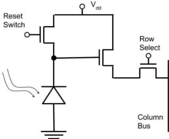
The architecture of a frameless pixel is given in Fig.3.1. Unlike conventional CMOS sensors, frameless pixel has an integrated comparator that resets the photodiode when the photons are accumulated to a threshold value, which results in a spike in the output voltage. The circuit implementation for a frameless pixel is shown in Fig.3.2. And sample diagram of the voltageVD andVoutas a function of time with varying light intensity is given in Fig.3.3.
The prescaler/decimator is a simple frequency divider that transmits one spike event to the column readout for every 2Dspikes; thus, it avoids sending too many events to the column. If the time interval between spike events
Chapter 3. Background: Frameless Image Sensor 21
FIGURE3.2: Frameless pixel circuit implementation
Chapter 3. Background: Frameless Image Sensor 22
from column is∆T:
light intensity∝ 2 D
∆T. (3.1)
3.2
Advantages
The frameless design will have the following benefits over those traditional framed capture architectures [10]:
• Frameless capture: each pixel’s saturation time is independently mea-sured.
• Wider dynamic range: More time for accumulating photons means longer exposure time.
• Greater precision: Time measurement is much more precise than pho-ton accumulation, yielding intensity values with precision of 20 bits.
23
Chapter 4
Improvement 1: Low-Light
Detection via Noise Reduction
4.1
Challenge: Noise
In low light regime, noise overwhelms the small low-light signal. The noise floor limits the camera performance because signal measurements less than noise floor are unreliable. However, many astronomy applications ask for cameras that are able to work in that “noisy zone”. Therefore, decreasing the noise level is the critical step to improve the camera performance, even for the frameless sensor. The limiting factor for low-light pixel performance is the kTC reset noise.
4.1.1
kTC Reset Noise
The reset noise, also known as kTC noise, is the noise introduced when reset-ting the capacitor. The purpose of a reset operation is to provide a reference level for comparison with the number of electrons generated from photons incident to the photodiode. The reset noise originates from the thermal noise that causes voltage fluctuations in the reset level. As a result, the reset voltage is a random variable that has a mean equal toVresetand a standard deviation equal to the reset noise√kT/C. Here, T is the temperature,k is Boltzmann constant, andC is the capacitance. A noisy reset operation undermines the pixel performance especially in low light level conditions because of an in-creased noise floor. The misplacement of a single electron can typically gen-erate 50µVof noise across a capacitance of 3fF[2]. This is a significant change in voltage compared to the generated signal and a major problem for most CMOS-based sensors.
4.2
Approaches to Mitigate Reset Noise
4.2.1
Noise subtraction via two-threshold sampling
Chapter 4. Improvement 1: Low-Light Detection via Noise Reduction 24
FIGURE4.1: Circuit implementation of the two-threshold sam-pling.
Chapter 4. Improvement 1: Low-Light Detection via Noise Reduction 25
FIGURE4.3: Circuit implementation of a pulse generator.
of VD drops to cross either of the threshold values (i,e. Vh/Vl), the output of the corresponding comparator changes from 0 to 1. The pulse generators convert the comparator outputs to spikes when the signals change from 0 to 1. Finally, the OR gate combines the spikes from the two pulse generators and outputs the combined signal.
The two thresholds will produce two spikes on the output for a single operation cycle. The two spikes can be tagged with a single bit to distinguish between signals from thresholdVl orVh. An example graph of howVD and
Voutchange over time is shown in Fig.4.2. The intensity can now be correctly calculated from the two known crossing points.
There are two regimes of operation. Under low light regime, the prescaler is typically not used because the frequency of pulses is low; therefore, both spikes from one operation cycle get through to the column pipeline. The pro-cessing logic will then subtract the time stamps of the two spikes. Under high light regime, the prescaler will always get rid of the first threshold crossing because the frequency of pulses is high. The whole operation effectively re-verts to the original operation when there is only one single threshold. Since many spikes are generated, the reset noise is automatically averaged.
The pulse generator can be implemented using the circuit diagram given in Fig.4.3, where the capacitance of the capacitor can be adjusted to set the width of spikes.
4.2.2
Noise averaging via repeated sampling
Because the reset noise is random noise by nature, it averaged out when the sample size is large. Therefore, speeding up the spike events together with using the prescaler for averaging can effectively reduce the reset noise by increasing the sample size.
Chapter 4. Improvement 1: Low-Light Detection via Noise Reduction 26
FIGURE4.4: Circuit implementation of the repeated sampling.
Chapter 4. Improvement 1: Low-Light Detection via Noise Reduction 27
FIGURE4.6: Simple current mirror circuit.
The current source is a well known analog circuit. we can match every pixel current with one reference current throughout the sensor chip using the current mirror circuit shown in Fig4.6. The circuit circled by dotted line is common to every pixel and is placed off pixel array.
4.2.3
Combined approach
The problem of using the two-threshold sampling alone for low-light envi-ronment is that some pixels can be too dark to provide spikes that are tem-porally meaningful, that is, failing to capture immediate information. When the two-threshold and repeated sampling methods are combined, the major benefit of this combined approach is the increase in the spike frequency for two-threshold sampling even under extreme low-light conditions. The cir-cuit implementation is given in Fig.4.7.
Chapter 4. Improvement 1: Low-Light Detection via Noise Reduction 28
4.3
Summary
29
Chapter 5
Improvement 2: Single Photon
Detection
5.1
Single-Photon Avalanche Diode (SPAD)
Imple-mentation
As introduced in Section 2.3.3, SPADs can detect the arrival of a single pho-ton. Such single photon sensing is beneficial for imaging in astronomy be-cause the targets are so faint that from them each pixel can only collects dozens of photons. By implementing SPADs into the frameless camera archi-tecture, we can identify the timestamp of the arrival of individual photons based on the spikes, and obtain valuable time series information on those stars from which the photons came.
5.1.1
Circuit Design
To make possible the single photon detection, the implementation of SPAD also requires an accompanying quenching circuit that distinguishes the avalanche. It can be divided into two categories: passive quenching and active quench-ing. The passive quenching scheme is composed of a simple resistor or properly biased transistor that slowly drains the avalanche current until the avalanche is turned off. Then, within the resistance-capacitance time con-stant of the circuit, the device is recharged to the full voltage.
Active quenching, on the other hand, is triggered by some electronics that sense the occurrence of an avalanche and turning off the SPAD immediately. The device is recharged for the next detection more quickly than passive quenching, reducing the dead time. It also suppresses the overall amount of avalanche current and therefore decreasing the afterpulsing probability, which is the probability of additional correlated avalanches caused by the charges trapped inside deep levels rather than photo-generated charges.
Chapter 5. Improvement 2: Single Photon Detection 30
FIGURE5.1: Circuit implementation for single photon detection using SPAD.
Chapter 5. Improvement 2: Single Photon Detection 31
across the SPAD so that avalanche is effectively distinguished. The pulse generator can be implemented using the same circuit shown in Fig.2.3.4.
Fig.5.2 shows how the voltages at a, b, and the output change after the occurrence of a single photon. The voltage at point a is the anode voltage of SPAD, while the SPAD’s cathode is held constant atVDD. Point b is con-nected directly to the output of pulse generator, and the width of the pulse can be set by adjusting the capacitance inside the pulse generator.Voutis the output of the comparator. Between the comparator’s output switching to 1 and the pulse generator producing a pulse, there is a small time delay and it is exaggerated in Fig.5.2.
We can see after the avalanche begins but before the left transistor is turned on, the voltage at point a rises rapidly from zero. This is when the avalanche occurs. Then, when left transistor is turned on, the voltage at point a is set toVo f f, which decreases the voltage across the SPAD to a value be-low the breakdown voltage and turns off the avalanche immediately. After an active quenching time determined by the pulse generator, the voltage at point b is low again so that the left transistor is turned off but the transistor connected to the ground is turned on. This time, the voltage at point a is lowered to zero which quickly recharged the SPAD. AfterVout is low again, the pixel is ready for another detection.
5.1.2
Challenges
Single photon detection can be a powerful feature for frameless image sen-sors, but the implementation of SPAD also raises many challenges.
• The photon detection probability (PDP) is limited even in visible spec-trum.
• The dark count rate (DCR) grows exponentially with temperature, which requires a low operating temperature down to−40◦C to get a DCR less than 10.
• Applying a higher voltage improves PDP, but also increases the DCR.
32
Chapter 6
Summary and Conclusion
In this work, we reviewed the basics of image sensors and conventional CCD and CMOS imaging technologies. Built upon a frameless camera architecture proposed in [10], we introduced several enhancements to the frameless sen-sor design to improve its low-light performance. Specifically, three methods for noise reduction are introduced: the two-threshold sampling that subtracts the noise, the repeated sampling that averages the noise, and a combined ap-proach for extremely low-light imaging. We also introduce the single photon detection by implementing the single-photon avalanche diode to detect the arrival of a single photon. These improvements aim at improving the perfor-mance of the frameless image sensor under the low-light condition typical for astronomy.
6.1
Comparison
Table 6.1 shows a comparison among conventional CCD and CMOS sensors and our new frameless image sensors with or without the noise reduction or the single photon detection functionality that I introduced. The low-light sensitivity, the performance under bright domain, the dynamic range, the reset noise (noise floor), and the availability of time-series information and pixel accessibility are compared. We can see the frameless image sensor not only greatly improves the dynamic range and thus the bright-domain opera-tion, but also makes the time-series information available. However, frame-less imaging with single photon detection presumably does not suit the op-eration in brightly-lit environment because the frequency of the pixel signals can easily reach the upper bound due to the overwhelming photons, which makes bright pixels indistinguishable. On the other hand, photons arriving at the same time can only be counted once, resulting in the loss of precision. But the introduction of single photon detection frees the camera sensor from reset noise, and makes each pixel sensitive to a single photon, suitable for operations in low-light environment.
Chapter 6. Summary and Conclusion 33
CCD CMOS Frameless
Frameless +noise reduction Frameless +single photon detection Dynamic range Blooming
smearing Moderate Good Good Good
Bright domain
Blooming
smearing Moderate Good Good
Not suitable Reset
noise Low High High Low
Not a concern
Low-light
sensitivity Good Limited Limited Improved
Sensitive to a single
photon Pixel
accessibility No Yes Yes Yes Yes
Time-series
information No No Yes Yes Yes
TABLE6.1: Comparison among CCD, CMOS, frameless, frame-less with noise reduction, and frameframe-less with single photon
de-tection image sensors.
6.2
Future work
Future work should first focus on the circuit simulation to check the integrity of the circuit design. Specifically, the noise level for the frameless pixels us-ing different noise-reduction methods should be checked and optimized. For single photon detection, the trade-offs between the key parameters of SPADs and the dark count rate should be studied during simulation for further op-timization. All the simulation should consider different lighting conditions and light spectra of interest.
34
Bibliography
1. <http : / / webee . technion . ac . il / labs / vlsi / Projects / PR210 / eeigor_APS_e.files/> (2012).
2. Calizo, I. G. Reset noise in CMOS image sensors (2005).
3. Clark, R. N.Digital Camera Reviews and Sensor Performance Summary(Oct. 2016). <http : / / www . clarkvision . com / articles / digital . sensor . performance.summary>.
4. El Gamal, A.Introduction to Image Sensors an Digital CamerasApr. 2001. 5. Fellers, T. J. & Davidson, M. W. CCD Noise Sources and Signal-to-Noise
Ratio (). <http : / / hamamatsu . magnet . fsu . edu / articles / ccdsnr . html>.
6. Fellers, T. J. & Davidson, M. W.Digital Camera Readout and Frame Rates(). <http://hamamatsu.magnet.fsu.edu/articles/readoutandframerates. html>.
7. Fossum, E. R. Active pixel sensors: are CCDs dinosaurs?1900. doi:10. 1117/12.148585. <https://doi.org/10.1117/12.148585> (1993).
8. Sapoval, B. & Hermann, C.Physics of semiconductorsISBN: 9780387940243. <https : / / books . google . com / books ? id = P6wPAQAAMAAJ> (Springer-Verlag, 1995).
9. Shockley, W. The theory of p-n junctions in semiconductors and p-n junction transistors. The Bell System Technical Journal 28, 435–489. ISSN: 0005-8580 (July 1949).
10. Singh, M., Zhang, P., Vitkus, A., Mayer-Patel, K. & Vicci, L. A Frame-less Imaging Sensor with Asynchronous Pixels: An Architectural Evaluation
in2017 23rd IEEE International Symposium on Asynchronous Circuits and Systems (ASYNC)(May 2017), 110–117. doi:10.1109/ASYNC.2017.19. 11. Tabet, M. Double sampling techniques for CMOS Image Sensors (Jan.
2002).
12. Theuwissen, A.Solid-State Imaging with Charge-Coupled DevicesISBN: 9780792334569. <https : / / books . google . com / books ? id = dchEKTHNCMcC> (Springer
Netherlands, 1995).