Research Article
July
2017
Computer Science and Software Engineering
ISSN: 2277-128X (Volume-7, Issue-7)
A Comparative Study of Low Power Testing Techniques for
Digital Circuits
Suhas B Shirol, Rajashekar B Shettar
Department of Electronics & Communication Engineering, B V Bhoomraddi College of Engineering & Technology, Vidhyanagar, Hubballi, Karnataka, India
DOI: 10.23956/ijarcsse/V7I7/0180
Abstract— In recent years, with fast growth of mobile communication and portable computing systems, design for low power has become the challenge in the field of Digital VLSI design. The main focus of the paper is to make a comparative study of low power Linear Feedback Shift Register (LFSR) architecture such as Built In Self Test (BIST), it has been often seen that during test mode process the power consumed is much higher, when compared to that of normal mode process test as there is high switching activity in the nodes of Circuit Under Test(CUT) during testing.
Keyword— Linear Feedback Shift Register(LFSR),Built In Self Test(BIST)Circuit Under Test(CUT), Automatic Test Equipment(ATE)Signature Analyzer(SA),Test Pattern Generation(TPG),Artificial Intelligent (AI).
I. INTRODUCTION
In recent years, with the advance of semiconductor manufacturing technology, the requirements of digital Very-Large-Scale-Integrated (VLSI) circuits, which are composed of billion‟s of gates, have given rise to many challenges during manufacturing test [1]. The power dissipated is substantial during test data for the large and complex chips, which greatly increases the system cost [2]. The low correspondence among test vectors raise switching activity and ultimately leads to power dissipation in the circuit. Built In Self Test (BIST) is the most suitable approach for low power testing as it provides a large scope for low power techniques to be used. BIST uses the LFSR as test pattern generator [3][4]. The LFSR generates all possible test vectors with a proper use of tap sequence. The test vectors reordering techniques aim to reduce the switching activity by modifying the order in which the tester applies the test vectors to the Circuit Under Test (CUT). Fault coverage is not affected by reordering of test vector, just their order is modified. Test cost can be reduced by improving use of test parameters [5]. These parameter are the test power, test length, test hardware overhead and test fault coverage. Page Layout
An easy way to comply with the conference paper formatting requirements is to use this document as a template and simply type your text into it.
II. BIST A. Built In Self Test
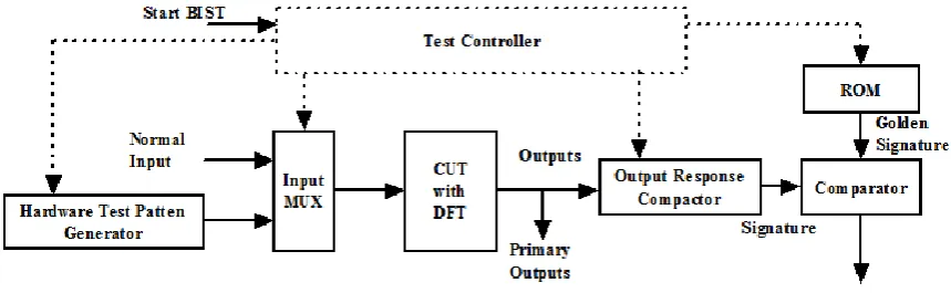
In modern chip design the complexity is very high, external testing with Automatic Test Equipment(ATE) become extremely expensive. Instead, built-in self-test (BIST) [6,7,8] has became more common in the testing of VLSI digital circuits As, it can overcome the problem of using external testing such as ATE. Test patterns generated by BIST are generated internally using parts of the circuit as in case of ATE instead they are generated externally, also the responses are analyzed using other parts of the circuit. When the digital VLSI circuit are in test mode, test patterns generators (TPGs) generate different patterns that are applied to the CUT, while the signature analyzer (SA) evaluates the CUT responses. One of the most common TPGs for exhaustive, pseudo-exhaustive, and pseudorandom TPG is the linear feedback shift register (LFSR) [9]. LFSRs are used as TPGs for BIST Architecture as shown in Figure(1) ,Generating all possible output test vector with little overhead in hardware area, use of appropriate XOR gate at appropriate location, the LFSR can generate all possible output test vector. The LFSRs posses the pseudorandom properties which leads to high fault coverage when a set of some test vectors is applied to the CUT compared with the fault coverage obtained using counters as TPGs. Also LFSRs can be configured to act as signature analyzers for the responses obtained from the CUT. Despite their simple appearance, LFSRs are based on complex mathematical theory that helps explain their behavior as TPGs or SAs.
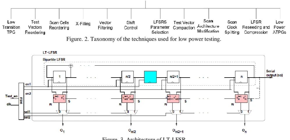
III. LOW POWER TESTING TECHNIQUES Taxonomy of the techniques used for low power testing[3] is shown in figure (2).
A. Low Transition Test Pattern Generation(LTTPG)
ISSN(E): 2277-128X, ISSN(P): 2277-6451, DOI: 10.23956/ijarcsse/V7I7/0180, pp. 412-418 found for ISCAS‟85 and ‟89 standards, corroborate that 77% reduction in average and 49% reduction in peak power, respectively[4]. The architecture used for the design of LT-LFSR is as shown in Figure(3).
B. Test Vector Reordering
Test vector reordering for combinational circuit testing for dynamic power minimization is major sub-problem for the low power testing. The reordering is the technique in which the applied sequence of test vectors is altered in such a way that the power dissipation is reduced during testing. The two major components of power dissipation in CMOS digital circuits are static power dissipation, due to leakage current and dynamic power dissipation, due to switching activity. Artificial Intelligent (AI) architecture based approach is presented to reorder the test vectors such that the minimum switching activity occur while applying the test vector to Circuit Under Test(CUT) and hence the power dissipation during testing. In this approach the hamming distance between successive test vectors is used to reorder the sequence. AI based reordering algorithm is implemented in Matlab and experimented with ISCAS‟85 benchmark circuits. The results obtained after reordered test vector set minimized the testing power of the circuit, when compared with unordered test vector set. Results obtained from the proposed method reduces 34.56% of the peak power and 30.15% of average power when the reordered test vectors are used for testing. The algorithm used for the design of Test Vector Reordering is as shown below.
Reordering Algorithm:
Step 1: The algorithm maintains two sets. Open list: The nodes to be examined are maintained in the open list for keeping track. Closed list: The nodes which are already been examined are maintained in closed list for keeping track.
Step 2: Initially, the open list has track of the initial node and the closed list is empty. Each node k maintains the following: g(k) = the cost of getting from the initial node to k h(k) = the estimate, according to the heuristic function, of the cost of getting from k to the goal node. f(k) = g(k) + h(k)
Step 3: Keeping track of each node which use a pointer to its parent, so that afterward we can have the one of the best solution if found can be retrieved A-star has a main loop that repeatedly gets the node, call it k, with the lowest f(k) value from the open list. If k is the goal node then the solution is given by back tracking from k. Otherwise k is removed from the open list and added to the closed list next all the possible successor nodes of k are generated.
Step 4: For the each successor node k if it is already in the closed list and copy, there has an equal or lower f estimate, then safely discard the newly generated k and move on. Similarly, if k is already in the open list and copy there an equal or lower f estimate, then safely discard the newly generated k and move on[10].
C. Scan Cells Reordering
We now describe how scan cells depend on the test vectors. This is equivalent to reordering of Bit Positions of Test Vectors. As the inputs belonging to the same compatible set will share the same data, it is advantageous in terms of power consumption if the scan cells corresponding to these inputs are chained consecutively so as to reduce the number of transitions during scan. Thus, the first step of scan chain reordering is to put all of the scan cells corresponding to the inputs of each compatible set next to each other. We convert the problem to a Travel salesman Problem(TSP). we assume that each column of test set is a city and its (vertical) hamming distance to other columns is their distances and now we have cities and their distances as shown in Figure( 4). We use genetic algorithm to find the minimum cost in reordering scan cells[10].
Left figure shows original test set and right one shows reordered test set as its depicted original vertical transition is 21 and after ordering we decrease it to 9 transitions. When compared with conventional Automatic Test Pattern Generation (ATPG) algorithm such as DEFGEN we found out through the experimental results with ISCAS '85 and '89 benchmark digital circuits shows that 21 %e switching activity can be reduced up. The Switching activity is reduced significantly when compared with existing methods[11,12].
D. Low Power Transition X-Filling
The Low Power Transition – X filling (LPT-X) method is used to reduce the transition between the 0's and 1's where unknown bits were filled. Weighted Transition Metric (WTM) method is mainly used to estimate low test power in Digital VLSI circuits. This approach is suitable for achieving reduction in average power consumption by LPT-X filling method.
Weighted Transition Metric
ISSN(E): 2277-128X, ISSN(P): 2277-6451, DOI: 10.23956/ijarcsse/V7I7/0180, pp. 412-418 WTM = ∑ ((L-j) . (TPi,j XOR TPi,j+1)) - (1)
Where TPi,j is the present scan test pattern and TPi,j+1 is the next scan pattern in the design. If more number of scan test pattern is applied then WTM is also considered for Peak power (WTMP) and Average power (WTMA). Peak power is calculated by the maximum value of WTM in „n‟ number of scan test pattern. Average power is calculated by summing all test pattern with the average of „n‟ test pattern. Using ISCAS89 benchmark circuits the experimental results were conducted and achieves 83 percent of reduced average test power[13].
E. Vector Filtering
We can observe that as self-test progresses, the capability of detecting fault, pseudo-random test vectors generated by an Linear Feedback Shift Register decreases rapidly. Therefore, the detection of new faults by many of the pseudo-random test vectors may not detect additional faults and hence preventing the Circuit Under Test from being excited by these undesired vectors. For this purpose, a decoder can be used during BIST pattern generation to store the first and last vectors of each subsequence of consecutive nondetecting vectors to be filtered. Rather than just filtering the subsequence's of nondetecting vectors, it is also possible to filter all vectors that do not detect any faults [Manich 2000]. Using this approach, a register made of latches is used to control the transmission of test vectors from the LFSR to the CUT[14]. A filter module is used to provide the needed control signals to the register is shown in Figure(5).
F. Shift Control Techniques
Scan Shifting: Several techniques have also been proposed to reduce or cancel the switching activity in the CUT during scan shifting. The authors in [Huang 1999] the scan shifting technique in which the primary inputs to the Circuit Under Test is applied in such a way that, we try to find an input vector which is called as control vector and causing the switching activity in the combinational section of the Circuit Under Test is reduced. To determine this input control vector, a modified version of the D-algorithm is used. The method has achieved some reasonable reduction in average power consumption.
Modified scan cell shifting: Another technique proposed in [Hertwig 1998] is to modify each scan cell in the scan chain so as to block transitions at the scan cell outputs prevent all switching activity during scan shifting in the combinational section of the Circuit Under Test. The scan cell modification consists of adding a NOR gate and an additional fanout to the output of each scan cell in Figure(6). During scan shifting, the NOR gate prevents data in the scan cell from propagating to the combinational part of the CUT. This technique obviously is effective in test power reduction; however, it requires a significant area overhead and may degrade the circuit performance[14,15].
G. LFSRS Parameter Selection
Specific parameters of LFSR may affect the power consumption of the CUT. They are namely the seed and the characteristic polynomial of the LFSR. It is found that the Weighted Switching Activity (WSA) obtained for a given primitive polynomial of the LFSR strongly depends on the seed [16,17]. Further WSA count is free of the selection of primitive polynomial of LFSR. Therefore, it is more essential to select the best seed than selecting the characteristic polynomial. Since it is not critical regarding the power consumption in the CUT with the selection of characteristic polynomial, it is recommended to use the LFSR that needs the minimum number of XOR gates in its feedback since this will reduce area overhead and reduce the power consumption in the LFSR itself.
H. Test Vector Compaction
The concept of test vectors compaction can be defined as follows [1]: Suppose a test T for a stuck-at fault F in a combinational logic circuit C is generated. T consists of logic levels 0 and 1, with some unknown states X (either 0 or 1) being assigned to some primary inputs (PI‟s) of C. The PI‟s at X may be made known to either a 0 or a 1 without affecting the validity of T. Two tests, T1and T2 for stuck-at faults F1 and F2 in C, are compactable if each PI of C is: 1) assigned to the same logic level in both TI and T2, or 2) at X in at least one test (TI or T2). Thus, by repetitive application of the compaction operation, many tests (two or more) can be combined into fewer tests. As a result, the total number of tests that need to be applied with the same fault detection capabilities is reduced.
Static Compaction
The process wherein all independent tests Ti are allowed to be generated first, before compaction is carried out, is referred to as static test compaction. It pays to delay the process of fault simulation until after static test compaction, since fewer tests need to be simulated, thus resulting in a reduction in fault simulation costs[14].
Dynamic Comapction
ISSN(E): 2277-128X, ISSN(P): 2277-6451, DOI: 10.23956/ijarcsse/V7I7/0180, pp. 412-418 1. select the next untested fault in the fault list and initialize all PI‟s to X;
2. generate a test (using a test generation algorithm) for a selected fault by assigning 0 or 1 to some of the PI‟s; 3. select the next untested fault in the fault list (a fault that has not yet been attempted for test Ti;);
4. attempt generation of test (using a test generation algorithm) for selected fault by allowing assignment of 0 or 1 to only those PI‟s that are still at X;
5. if successful in generating a test in step 4, then go back to step 3;
6. apply heuristic criteria to evaluate the likelihood of detecting additional faults if PI‟s are still at X, then go to step 3 or, if not, continue;
7. set values 0 or 1 on the PI‟s still at X; 8. fault-simulate Ti;
9. repeat from step 1 to generate next test.
Current test generation algorithms differ in the way each of the general steps described is implemented. In particular, alternate techniques in Steps 3 and 6 result in improved performances, i.e., reduction in the test generation cost and reduction in the amount of test data (the number of test vectors) [18].
I. Scan Architecture Modification
Scan Architecture modification method in which during testing , peak power and average power dissipation is much less compared to normal mode in which higher switching activity within scan chain for scanning in/out of the vector/response pair. In this technique a method is proposed to reduce dynamic power consumption in scan chain by bring in XOR gate at selected places (using genetic algorithm) in the conventional scan chain there by converting D flip-flops into T flip-flip-flops temporarily during scan. This approach involves reordering of test vectors but not reordering of the scan cells. Our proposed method is verified with ISCA' 85 and ISCAS '89 benchmark circuits, which shows the experimental results upto 24% reduction in switching activity within modified scan architecture is possible[26].
J. Scan Clock Splitting
In the scan-chain. The use of such a system reduces the average peak power consumption without increasing test time. This technique modifies the scan clock in order to reduce the power consumption during scan testing . In [20] a technique based on scan clock splitting is presented. It involves reducing the operating frequency of the scan cells during scan shifting without modifying the total test time. In this technique, two clocks have been used; each of them is at half the frequency of the system clock, and is used to activate half of the scan cells uses a staggered clock scheme to reduce the peak power consumption during scan testing is presented in.
K. LFSR Reseeding Compression
Considering together the problems of test data compression and low power test is very important. A long sequence of test vectors which also means high energy consumption since the total energy is a function of time. Hence, compression of test data leads to reduction to the total energy. Furthermore, using clever techniques for the compression will also reduce the average and peak power consumption. The low power test data compression techniques can be divided into three main categories [21]: coding-based techniques, linear-decompression-based techniques (LFSR reseeding techniques) and broadcast-scan-based technique. For example found in [22]. In the test cubes generated by ATPG are encoded using Golomb codes which are developed from run-length codes. All don‟t care (X) bits are mapped to 0 and the Golomb code is used to encode runs of 0s. This technique is efficient to compress the runs of 0s but inefficient to encode the runs of 1s and the test storage may increase if there are many runs of 1s in the test cubes. The technique presented in [23] based on alternating run-length coding overcomes this problem. In [24] a method that uses dual LFSR reseeding technique is used to reduce total power by masking some bits in the test vector by using AND and OR gates, thus reducing the transition probability. However, the method needs a hardware area overhead and increases test storage since there are two LFSRs used in the technique. In [25] the authors present a scheme that uses a LFSR reseeding technique to reduce the number of transitions in the scan-chain with an acceptable area overhead and good test power reduction.
ISSN(E): 2277-128X, ISSN(P): 2277-6451, DOI: 10.23956/ijarcsse/V7I7/0180, pp. 412-418
Figure. 2. Taxonomy of the techniques used for low power testing.
Figure. 3. Architecture of LT-LFSR
Figure. 4. 6 node full graph
Figure. 5. Filter Module
ISSN(E): 2277-128X, ISSN(P): 2277-6451, DOI: 10.23956/ijarcsse/V7I7/0180, pp. 412-418 IV. CONCLUSION
In this paper a qualitative survey on low power testing techniques and its methodology was carried out. The major area of concentration was on average power and average peak for most of the testing techniques. While analyzing, all dimensions of power during chip testing was considered as parameters. Further this paper gives a survey on algorithmic side and hardware approaches.
ACKNOWLEDGMENT
I would like thank my guide for the consistent support and also thank my family for the support.
REFERENCES
[1] Sunghoon Chun, Taejin Kim and Sungho Kang, "A New Low Energy BIST Using A Statistical Code," IEEE,
pp. 647-652, 2008
[2] Lubna Naim and Tarana A. Chandel, “Design of Low Transition Pseudo-Random Pattern Generator for BIST
Applications,” International Journal of Computer Applications., vol. 87, no. 15, February 2014.
[3] Abu-Issa and S. Quigley, Bit-swapping LFSR and scan-chain ordering: A novel technique for peak- and
average-power reduction in scan-based BIST, IEEE Trans. Compute.- Aided Design Integral. Circuits Syst., vol. 28, no. 5, pp. 755–759, May 2009.
[4] Mehrdad Nourani, Mohammad Tehranipoor and Nisar Ahmed, “Low-Transition Test Pattern Generation for
BIST-Based Applications,” IEEE Transactions on Computers., vol. 57, no. 3, pp. 303-315, March 2008.
[5] Praveen J, and M N Shanmukhaswamy, “Power Reduction Technique in LFSR using Modified Control Logic
for VLSI Circuit,” International Conference on Electronic Design and Signal Processing (ICEDSP) 2012.
[6] V. Agrawal, C.R. Kime, and K. Saluja, "A tutorial on built-in self-test - part 1: principles", IEEE Design and Test of Computers, pp. 73-82, March 1993.
[7] V. Agrawal, C.R. Kime, and K.K. Saluja, "A tutorial on built-in self test - part 2: applications", IEEE Design and Test of Computers, pp. 69-77, June 1993.
[8] V. Agrawal, C.-J. Lin, P.W. Rutkowski, S. Wu, and Y. Zorian, "Built-in self-test for digital integrated circuits", AT&T Technical Journal, pp. 30-39, March 1994.
[9] P.H. Bardell, W.H. McAnney, and J. Savir, Built-in test for VLSI: pseudorandom techniques, John Wiley & Sons, 1987.
[10] Mehdi Salmani Jelodar, Kiarash Mizanian, " Power Aware Scan-based Testing using Genetic Algorithm," IEEE CCECE/CCGEI, Ottawa, May 2006
[11] S. Chakravarty and V. Dabholkar, “Minimizing Power Dissipation in Scan Circuits During Test Application”,
IEEE International Workshop on Low Power Design, 1994, pp. 51-56.
[12] P. Girard, C. Landrault, S. Pravossoudovitch and D. Severac, “Reducing Power Consumption during Test Application by Test Vector Ordering,” IEEE Intl. Symposium on Circuits and Systems, 1998, pp. 296-299.
[13] P. Raja Gopal , S. Saravanan, " Low Power Estimation on Test Compression Technique for SoC based Design, " Indian Journal of Science and Technology, Vol 8(14), July2015
[14] M. Abramovici, M.A. Breuer, and A.D. Friedman, Digital Systems Testing and Testable Design, IEEE Press,
1990.
[15] N.-C. Lai and S.-Y. Wang, "Low-capture-power test generation by specifying a minimum set of controlling inputs", Asian Test Symposium, pp. 413-418, October 2007.
[16] P. Girard, L. Guiller, C. Landrault, S. Pravossoudovitch, J. Figueras, S. Manich, P. Teixeira, and M. Santos, "Low energy BIST design: Impact of the LFSR TPG parameters on the weighted switching activity", Proceedings of International Symposium on Circuits and Systems, pp. 110-113, June 1999.
[17] M. Brazzarola and F. Fummi, "Power characterization of LFSRs", International Survey on Defect and Fault Tolerance in VLSI Systems, pp139-147, November 1999.
[18] B. Ayari and B. Kaminska, “A New Dynamic Test Vector Compaction for Automatic Test Pattern Generation”,
IEEE, Trans. on Computer-Aided Design of Integrated Circuits and Systems, vol. 13, no. 3, March 1994. [19] Giri, C., Choudhary P.K. , Chattopadhyay S., "Scan Architecture Modification with Test Vector Reordering for
Test Power Reduction ," International Symposium on Integrated Circuits, ISIC '07, 2007
[20] R. Sankaralingam and N. Touba, "Multi-phase shifting to reducing instantaneous peak power during scan", Proceedings of Latin American Workshop, pp. 78-83, February 2003.
[21] L.-T. Wang, C.-W. Wu, and X. Wen, VLSI Test Principles and Architectures: Design for Testability, San Francisco, Morgan Kaufmann, 2006.
[22] Chandra and K. Chakrabarty, "Combining low-power scan testing and test data compression for system on-a-chip", Proceedings of Design Automation Conference, pp. 166-169, June 2001.
[23] Chandra and K. Chakrabarty, "Reduction of SOC test data volume, scan power and testing time using alternating run-length codes", Proceedings of Design Automation Conference, pp. 673-678, June 2002.
[24] P. Rosinger, B.M. Al-Hashimi, and N. Nicolici, "Low power mixed-mode BIST based on mask pattern generation using dual LFSR- reseeding", Proceedings of International Conference on Computer Design, pp. 474-479, 2002.
ISSN(E): 2277-128X, ISSN(P): 2277-6451, DOI: 10.23956/ijarcsse/V7I7/0180, pp. 412-418
[26] Chandan Giri, P.K. Choudhary and Santanu Chattopadhyay "Scan Power Reduction Through Scan
Architecture Modification And Test Vector Reordering, " ASIAN TEST SYMPOSIUM , NOVEMBER 2007.S.
M. Metev and V. P. Veiko, Laser Assisted Microtechnology, 2nd ed., R. M. Osgood, Jr., Ed. Berlin, Germany:
Springer-Verlag, 1998.
AUTHORPROFILE
Suhas B Shirol, is an Assistant Professor at the Department of Electronics & Communication Engineering, B V Bhoomraddi College of Engineering and Technology. His research interest is in the area of Digital VLSI, SoC Verification, Embedded Systems.