RADIOACTIVE THORIUM-DOPING EFFECTS ON THE
SPECTRAL AND ELECTRICAL FEATURES OF Th-DOPED
212-VANADATE CERAMICS
Khaled M. Elsabawy
[a,b]and Morsy M.Abou-Sekkina
[a]Keywords: Thorium doping; Perovskite; Th-doped 212-vanadate ceramics;
The compounds with general formula Bi2SrV2-xThxO9, where (x=0.05, 0.1, 0.2, 0.3, 0.6) were carefully synthesized and processed by using mixed techniques solid state reaction and solution routes with sintering temperature at 880 °C for 20 h. XRD – analysis of the prepared samples proved that thorium(IV)-dopant can substitute successfully until x=0.55 mole on the Bi-layered perovskite crystal structure without damaging the original perovskite structure . It was observed that Th-dopings have slight to moderate effects on both ESR-signals and conduction mechanism of Th-doped Bi-Sr-V-O regime. Electrical measurements indicated that the energy gap Eg and number of electrons in conduction band Ncb increase as the ratio of Th doping increases from x=0.05 till x=0.6 mole respectively due to the increasing of paramagnetic character of thorium than vanadium .
* Corresponding Authors Tel: +9660503252190
E-Mail: [email protected]
[a] Materials Science Unit-Chemistry Department-Faculty of Science-31725-Tanta University-EGYPT
[b] Materials Science Unit,Faculty of Science,Taif University-Taif City-Alhawyah-888-Saudi Arabia
Introduction
The multi-layered perovskite structural materials such as Bi-Sr-V-O have attracted increasing attention in the research community because they are fatigue – free and lead free1-3 . The wide spread application and commercialization of bismuth- layered perovskite ferroelectrics have been limited due to drawbacks, as high processing temperature and relatively low remanent polarization4-5 . Recently, efforts have been made to enhance the properties of layered perovskite ferroelectrics by addition or substitution of alternative cations6-8 . It's now well established that the variation of oxygen content and distribution of oxygen atoms on the lattice site strongly influences the physical and structural properties (e.g. electrical conductivity) at high-temperature, as superconductors and many other metallic oxides9 .
The discovery of high temperature superconductors has drawn much attention for their technological application such as superconducting quantum interference devices (SQUID), the high Tc ceramic super-conductor, the Bi– based system has been studied because of its high critical temperature especially with the partial substitution of Pb in Bi and Sr sites since it promotes the stabilization of 2223 phase when grown from 2212 phase10-11.
Many published reports12-14 are explaining the discovery of mixed metal oxides having bismuth layer alternating with perovskite structure layers, because of their ionic
structural framework, Aurivillius phases exhibit great flexibility with respect to metal cation substitution. Therefore, these phases have high potential for systematic control of their properties15.
There are various studies showing the chemical substitution such as Pb doping on Bi-O layers that can be used to improve conduction in the blocking layers and so as to large decrease in the resistivity anisotropy. The reduced anisotropy leads to improvement of the critical current in the heavy Pb-doped16-21.
Das et al.22 reported the improved remanent polarization of SBN and SrBi2Ta2O9 this films, when a small amount of Ca cations were incorporated into A sites: Bismuth layered perovskite materials have high fatigue resistance23,24.
The crystal structure and chemical composition of these layered perovskites were systematically studied25 with the general formula of (Bi2O2)2+ (Am-1BmO3m+1)3- , consisting of m-perovskite unites sandwiched between bismuth oxide layers called the family of bismuth layered structured ferroelectrics26, where A and B two types of cations that enter the perovskite unite A is Bi3+ , Ba2+ , Sr2+ , and B is Ti4+,Ta5+ , and m=1-6 layered perovskite strontium tantalite is a member of bismuth layer- structured ferroelectrics.
The crystal structure of Sr Bi2Ta2O9 comprises pseudo- perovskite blocks (SrTa2O7)2- that are sandwiched between (Bi2O2)2+ layers. Sr occupies the A site of the perovskite block and Ta occupies the B-site27.
Experimental
The pure perovskite compound Bi2SrV2O9 and different Th-doped samples with the general formula Bi2SrV2-xThxO9, where x=0.05, 0.1, 0.2, 0.3, 0.6 mole were prepared by conventional solid state reaction and solution routes with sintering procedure using the appropriate amounts of Bi2(CO3)3, SrCO3, (NH4)2VO3 and ThO2 (each purity > 99%).
Thorium oxide is tested by Geiger counter of radioactivity, it was radioactive oxide with low emission. The mixture was grounded in an agate mortar for one hour then dissolved in few drops of concentrated nitric acid then dilution process was made with adjusting pH-value by 30% ammonia solution. The obtained solution was divided into two portions out of which one portion was treated by 0.4 M oxalic acid and the other one by ammonium carbonate of 0.4 M respectively.
M(NO3)n+(n/2)H2C2O4→M(C2O4)n/2↓+n/2HNO3 (1)
M1(NO
3)n + n/2(NH4)2CO3 + xH2O → NH4NO3
+(n-x)/2CO2M(OH)x(CO3)(n/2-2x) (2)
where M=Bi, Sr, V and Th(IV) ions, respectively .
The result metals precipitates (as oxalates, basic carbonates and hydroxylated oxides) were collected and dried in oven at 80 oC .Then the finely grounded powder was subjected to heat at 800 oC for 10 hours, regrounded and finally pressed into pellets with thickness 0.2 cm and 1.2 cm diameter and sintered at 880 oC for 20 hours. Then the furnace is cooled down slowly to room temperature. Finally the materials are kept in vacuum desiccator over silica gel dryer.
Structural Measurements
X-Ray diffraction (XRD)
The X-ray diffraction measurements (XRD) were carried out at room temperature on the fine grounded Bi2SrV2O9 and Bi2SrV2-x ThxO9 systems in the range (2θ =10-80o) using Cu-Kα radiation source and a computerized [Bruker Axs-D8 advance] X-ray diffractometer with two theta scan technique.
Conductivity Measurements
The DC-electrical conductivity of the samples was measured using the two terminals DC-method. The pellets were inserted between spring loaded copper electrodes, A KEITHLEY 175 multimeter (ASA) was employed from room temperature up to 500K. The temperature was measured by a calibrated chromel-alumel thermocouple placed firmly at the sample. Measurements were conducted in such a way that at each temperature, sufficient time was allowed to attain thermal equilibration.
Solid infrared absorption spectral measurements
The IR absorption spectra of the prepared samples were recorded using "Nexus 670 FT IR spectrometer in the range 500-2500 cm-1 using pure KBr matrix".
Electron paramagnetic resonance measurements
The electron spin resonance spectra (ESR) were recorded at room temperature for the prepared samples using at x-band frequencies on a "Bruker- ELEXSYS E 500 Germany" spectrometer.
Results and Discussion
X-Ray Diffraction
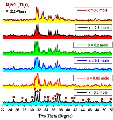
The X-ray diffraction patterns of pure and variant Th-doped samples with the general formula Bi2SrV2-x ThxO9, where x= 0.05, 0.1, 0.2, 0.3, 0.6 mole are shown in Fig. 1.a-f. Analysis of the corresponding 2θ values and the interplanar spacing d (Ao) by using computerized program proved that the compound is mainly belongs to distorted perovskite type with hexagonal crystal form, that expressed by assigned peaks in major. The unit cell dimensions were calculated using parameters of the most intense X-ray reflection peaks and found to be a= b= 5.7984 Å and c= 7.2124 Å for the pure 212Bi-Sr-V-O. Single phase of the layered perovskite structure appeared when M4+ is up to or equal to 0.05.28 The substitution of Th4+ for V5+ in BSV would induce A-site cation vacancies in perovskite layers, which leads to an increase of internal stress for the shrinkage of unite cell volume as reported.29 The increasing number of tetravalent thorium ions in the crystal lattice of BSV will result in strong stress, which will expel other Th-ions from the crystal lattice of BSV(212-Bi-V-O) causing some extent of distortion on the perovskite layers .
Fig (1a-f): XRD patterns recorded for (a) pure Bi2SrV2O9 and
Th-doped samples (b):Bi2SrV1.95Th0.05 O9 , (c):Bi2SrV1.9 Th0.1 O9, (d):
Bi2SrV1.8Th0.2 O9, (e):Bi2SrV1.7Th0.3O9, (f):Bi2SrV1.4Th0.6O9
22 24 26 28 30 32 34 36 38 40 42 44 46 48 50 52
Bi2SrV2-xThxO9
Two Theta (Degree)
x= 0.0 mole x = 0.05 mole x = 0.1 mole x = 0.2 mole x = 0.3 mole
x = 0.6 mole
The layered perovskite structure would be more restrictive since (Bi2O2)2+ interlayeres impose a great constraint for structural relaxation. Such a structural constraint induced from (Bi2O2)2+ interlayeres may well explain the lack of an appreciable decrease in lattice parameters with an increased amount of vanadium dopping30.
Figure 2. Variation of c-axis as a function of Th-content.
From Fig.2 it is clear that c-axis increases as a result of substitution Th-dopant. On the bases of ionic radius it is expected that c-axis increases as Th4+ doping ratio increases. Furthermore, Th4+ is lower in charge than V5+ and as a result of which it is expected to decrease stress inside lattice and consequently the shrinkage factor of lattice will be increased. From Fig.1a-f, it is clear that the Th-substitutions are successful in the most of investigated range even at high concentration x=0.6 mole since there is no evidence noticeable at X-ray diffractogram referring to Th-impurity phase which reflects that all doping ratios are within the internal lattice structure. This confirms that Th-dopant can substitute in the V-sites successfully in the whole investigated range.
Figure 3a, 3c and 3e. ESR spectra at room temperature for pure and some selected Th-doped 212-Bi-Sr-V-O system where (a): Bi2SrV2O9, (c): Bi2SrV1.9Th0.1O9 and (e): Bi2SrV1.7Th0.3O9
Electron paramagnetic resonance measurements
Fig. 3a, 3c and 3e explain the electron spin resonance (ESR) signals recorded for pure Bi-212-vanadates and some selected thorium doped samples with x=0.1 and 0.3 mol.
It was shown that the effective g-values (giso) exhibit an increase from x=0.0 mole to x=0.3 mol due to strong interaction of coupling between Th4+ ion that substitutes V5+ ion successfully at low dopant concentration as shown in Fig. 4.
These results of ESR-spectra proved that the anisotropy occurred as a result of increasing of Th doping is due to the increasing of paramagnetic character of substituted vanadates where geff varies as function of x value.31,32,33
Figure 4. Variation of Giso versus Th-content .
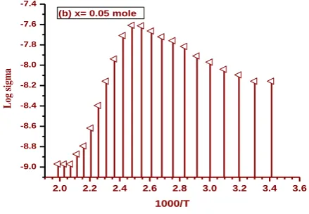
DC-Electrical conductivity measurements
Fig.5a-f displays the variation of DC-electrical conductivity as a function of reciprocal of absolute temperature for various Th4+ dopings. The data from Fig.5a-f exhibit conducting and semi-conducting behavior since the conductivity increases with an increase in temperature in case of conductor and conductivity decrease with an increase in temperature in case of semiconductor.33
Fig. 6a and 6b show the relation between the energy gap (Eg)
,
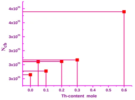
number of e- in conduction band (Ncb) for Th-doped samples, in which both of Eg and Ncb increase as the ratio of Th-doping increases from x = 0.05 to x = 0.6 mole, which may attributable to the numbers of unpaired electrons in the thorium outer shell which is higher than those of existed in the vanadium ions .0,0 0,1 0,2 0,3 0,4 0,5 0,6
7,10 7,12 7,14 7,16 7,18 7,20
c
-a
x
is
A
o
Th-Dopant Ratio mole
0 1000 2000 3000 4000 5000 6000
Field (G) a
In
te
n
s
it
y
(a
.u
)
c e
0.00 0.05 0.10 0.15 0.20 0.25 0.30
2.28 2.29 2.30 2.31 2.32 2.33 2.34
Giso
Th-content mole
0 (3)
g
E
kT
e
3/ 2 2 (4)
g
E
kT cb
N AT e
where A = constant, Eg = energy gap in eV, k = Boltzmann constant and finally Nc = numbers of electrons in the conduction band in electrons unit .
Furthermore, the energy gab in the thorium band structure is lower than that of vanadiun and as result of it a number of electrons evaluated in the conduction band Nc are increasing as thorium dopings increase .
Figure 5a. Variation of DC- electrical conductivity as a function of temperature for pure212-Bi-Sr-V-O system
.
Figure 5b. Variation of DC- electrical conductivity as a function of temperature for (b) Bi2SrV1.95 Th0.05O9
.
Solid infrared absorption spectral measurements
The infrared absorption spectra of pure Bi2SrV2O9 and their thorium doped samples in the range of 500-2500 cm-1 are shown in Fig. 7.
It is well known fact that 212-Bi-Sr-V-O9±δ system is mainly belongs to deficient perovskite structures and an extra oxygen atom)O9 ± δ). Oxygen nine converts it to distorted perovskite structure and consequently the common vibrational modes of IR-spectra of perovskite are clearly appeared.
Figure 5c. Variation of DC- electrical conductivity as a function of temperature for (c) Bi2SrV1.9Th0.1O9
Figure 5d. Variation of DC- electrical conductivity as a function of temperature for (d) Bi2SrV1.8 Th0.2O9
.
Figure 5e. Variation of DC- electrical conductivity as a function of temperature for (e) Bi2SrV1.7Th0.3O9
.
1.8 2.0 2.2 2.4 2.6 2.8 3.0 3.2 3.4 3.6
-9.0 -8.8 -8.6 -8.4 -8.2 -8.0
Log
sigm
a
1000/T (a) x = 0.0 mole
2.0 2.2 2.4 2.6 2.8 3.0 3.2 3.4 3.6
-9.0 -8.8 -8.6 -8.4 -8.2 -8.0 -7.8 -7.6 -7.4
L
og si
gm
a
1000/T
(b) x= 0.05 mole
2.2 2.4 2.6 2.8 3.0 3.2 3.4
-9.0 -8.9 -8.8 -8.7 -8.6 -8.5
Log
sigm
a
1000/T (c) x = 0.1 mole
1.8 2.0 2.2 2.4 2.6 2.8 3.0 3.2 3.4 3.6
-9.0 -8.8 -8.6 -8.4 -8.2 -8.0 -7.8 -7.6
Log s
igm
a
1000/T (d) x = 0.2 mole
1.8 2.0 2.2 2.4 2.6 2.8 3.0 3.2 3.4 3.6 -9.0
-8.8 -8.6 -8.4 -8.2 -8.0 -7.8 -7.6
Log s
igm
a
1000/T
From Fig.7 we can summarize the different vibrational modes and their reasons as follows;
Figure 5f. The variation of DC- electrical conductivity as a function of temperature for (f) Bi2SrV1.6 Th0.4O9
Figure 6a. Variation of Egab versus Th–content.
(a) The range from 390-620 cm-1 includes the most of infrared active phonons involving stretching modes of vibrating Bi-O, Sr-O and V-O/Th-O plus bending modes of Bi-O-V, Bi-O-Sr, respectively.
Figure 6b. Variation of Ncb versus Th –content.
(b) The broad band around 800 cm-1 is mainly due to an increase in the free carrier scattering as reported in many previously published papers as reported in 34-35.
Figure 7. The room temperature solid infrared absorption spectra recorded for ; (a): Pure Bi2SrV2O9, (b): Bi2SrV1.95 Th0.05O9, (c):
Bi2SrV1.9 Th0.1O9, (d): Bi2SrV1.8 Th0.2O9, (e):Bi2SrV1.7 Th0.3O9, (f):
Bi2SrV1.4Th0.6O9
(c) The vibrational modes at ≈ 690-820 cm-1 is due to the effect of charge exchanging of V+5/Th+4 carriers which is enhanced by increasing paramagnetic character caused by Th-dopings.
Conclusions
In summary, 212-Bi-Sr-V-O ceramics with various Th-doping ratios were successfully synthesized by mixed solid state/solution routes. X-ray diffraction proved that the compounds have distorted perovskite structure with hexagonal crystal form and the Th-ions can substitute successfully even at high concentration as x=0.6 mole. The ferroelectric properties of the layered perovskite have been significantly enhanced with Th-doping. The DC-electrical studies show conducting and semi-conducting behavior. IR spectra indicated that the system is mainly belongs to deficient perovskite structure with an extra oxygen atom (O9±δ where δ less than 1).
References
1de Araujo, C. A. P. Cuchiaro, J. D. McMillan, L. D. Scott, M. C.
and Scott, J. F., Nature (London), 1995, 374, 627–29.
2Scott, J. F. and de Araujo, C. A. P., Science, 1989, 246, 1400–
1405.
3Cao, G. Z., In Advances in Materials Science and Applications.
Edited by D.L.Shi. Tsinghua University Press and Springer-Verlag, Beijing, China, 2001, 86–112.
4Scott, J. F., p. in Thin Film Ferroelectric Materials and Devices.
Edited by R. Ramesh. Kluwer, Norwell, MA, 1997, 115.
5Scott, J. F., Ann. Rev. Mater. Sci.,1998, 28, 79–100 .
6Duran-Martin, P., Castro, A., Millan, P., and Jimenez, B., J. Mater.
Res. , 1998, 13, 2565.
1.8 2.0 2.2 2.4 2.6 2.8 3.0 3.2 3.4 3.6
-9.0 -8.8 -8.6 -8.4 -8.2 -8.0 -7.8 -7.6 -7.4
Lo
g s
ig
m
a
1000/T
(f) x = 0.6 mole
0.0 0.1 0.2 0.3 0.4 0.5 0.6
0.00005 0.00010 0.00015 0.00020 0.00025 0.00030 0.00035
Ega
p
Th-content mole
0.0 0.1 0.2 0.3 0.4 0.5 0.6
3x1025 3x1025 3x1025 3x1025 4x1025 4x1025
Ncb
Th-content mole
0 500 1000 1500 2000 2500 3000 3500 4000 4500
Wavenumber Cm-1
(a) x = 0.0 mole
(b) x = 0.05 mole (c) x = 0.1 mole
(d) x = 0.2 mole
(e) x = 0.3 mole
7Torii, Y., Tato, K., Tsuzuki, A., Hwang, H. J., and Dey, S. K. J.
Mater. Sci. Lett., 1998,17, 827.
8Watanabe, H., Mihara, T., Yoshimori, H., and Araujo, C. A. P.,
Jpn. J. Appl. Phys. , 1995, 34, 5240.
9Shimoyama, J., Kasa, J., Morimoto, T., Mizusaki, J., Tagawa, H.,
Physica C, 1981, 185, 931 .
10Diaz-Valdes, E., Pacheco-Malagon, G., Contreras-Puente, G.,
Mejia, G. C., Andrade-Garay, G., Ortiz-Lopez, J., Conde-Gallardo, A., Falcony, C., Mater. Chem. Phys., 1993,36, 64.
11Hewitt, K. C., Chen, X. K., Meng-Burany, X., Curzon, A. E.,
Irwin, J. C., Physica C, 1995,251, 192.
12Aurivillius, B., Ark. Kemi, 1949, 1(58), 499-512 .
13Aurivillius, B., Ark. Kemi, 1949,1(54), 463-80. 14Aurivillius, B., Ark. Kemi, 1950,2(37), 519.
15Rentschler, T., Mater. Res. Bull., 1997,32(3), 351.
16Motohashi, T., Nakayama, Y., Ujita, T., Kitazawa, K.,
Shimoyama, J., Kishio, K., Phys. Rev. B, 1999, 59, 1408.
17Shimoyama, J., Nakayama, Y., Kitazawa, K., Kishio, K., Hirio,
Z., Chong, I., Takano, M., Physica C, 1997, 281, 69 .
18Wu, W. D., Keren, A., Le, L. P., Sternlieb, B. J., Luke, G. M.,
Uemura, Y. J., Phys. Rev., 1993 , B47, 8127 .
19Ma, Q. Z., Ca, G. H., Li, Y., Chen, N., China J. Low. Temp.
Phys. , 1996, 18, 246 .
20Ma, Q. Z., Huang, X. Q., Xiong, X. T., Li, Y., Cao, G. H., Zhang,
T. B., China J. Low Temp. Phys., 1997, 19, 128.
21Shrivastava, V., Jha, A. K., Mmendiratta, R. G., Physica B , 2001,
371, 337.
22Das, R. R., Bhattacharya, P., Perez, W., Katiyar, R. S., Ceram.
Int.2004, 30, 1175.
23de Araujo, C. A. P., McMillan, L. D., Cuchiaro, J. D., Scott, M. C.
and Scott, J. F., Nature(London)1995, 371, 631.
24Scott, J. F. and de Araujo, C. A. P., Science, 1989, 246, 4936. 25Aurivillius, B., Ark. Kemi., 1952, 5, 39–47.
26Subbarao, E. C., Phys. Rev., 1961,122(3), 804–807.
27Coondo, I., Jha, A. K., Solid state Communi., 2007, 142,
561-565 .
28Qiu, J., Liu, G. Z., He, M., Gu, H. S., Zhou, T. S., Physica B ,
2007, 400, 134-136.
29Coondoo, I., Sha, A. K., Aggawal, S. K., Soni, N. C., J.
Electroceram., 2006, 16, 393.
30Wu, Y., Cao, G., J. Mat. Res., 2000, 15, 86 .
31Onyszkieuicz, I., Czarnecki, P., Mienas, R., Robaszkiewiez, S.,
Physica, (B-C),1979, 147(2-3), 166.
32Hidaka, T., Phys. Rev. B, 1979, 20, 2769.
33Simpson A., Robert; E. Introductory Electronics for Scientists &
Engineers, 2nd Edition, Allyn and Bacon, UK, 1987. 34Memon, A., Khan M. and Adallal, S.; Physica C, 1994, 9,
235-240.
35Qurong P., Jie, G. X:, Zengming, Z. and Zejum, D., Physica C
2002, 70, 269-274.