DEVELOPMENT AND INTERGRATION OF HEART RATE
MEASUREMENT INTO THE STM32F4-BASED CM5 SYSTEM
Lili Xu
A thesis submitted to the faculty of the University of North Carolina at Chapel Hill in partial fulfillment of the requirements for the degree of Master of Science in the Department of
Biomedical Engineering.
Chapel Hill 2014
Approved by:
Mark Tommerdahl
Bob Dennis
© 2014 Lili Xu
ABSTRACT
LILI XU: Development and integration of heart rate measurement into the Stm32F4-based CM5 system.
(Under the direction of Dr. Mark Tommerdahl)
In this thesis, I report our research work on development of a new generation of
Cortical Metrics systems (CM), using the STM32F4 embedded system, and the development
and integration of a new heart rate measurement function into the new system. In this thesis, I
introduce the background of this project, the hardware system “STM32F4 Discovery Board”,
the compiling environment settings and the software I used. I report the test of proper
working conditions for the heart rate sensor---the pulse sensor, the signal processing method
for identification of heartbeats from the signal that coming out from the pulse sensor. I
discuss the conflicts of arranging recourses on the STM32F4 Discovery board, and present
our solution of how to integrate the heart rate module into the tactile stimulator system
reasonably, so that different modules of different functions in the tactile system could work
independently and effectively. Worked together with Dr. Holden Jameson, we also made the
communication between the heart rate module and the computer, and used three different
In sum, we successfully built a new heart rate module, and integrated the heart rate
module into the Cortical Metrics system. The new CM system with heart rate measurement
has been successfully tested and used by different users. We are looking forward to its further
application in scientific research of neuronal diseases and looking for its test with more
DEDICATION
To my parents and parents in law, who supported and encouraged me during the time
studying at USA.
And to my husband, Zaozao, who gives endless support to me.
ACKNOWLEDGMENTS
The work presented in this thesis would not have been possible without the supports
from following people. I’d like to express my deepest gratitude and sincere appreciation to
all of them.
I am deeply and sincerely grateful to my advisor Mark Tommerdahl. You gave me a
great chance to work on an exciting new embedded system ---- the CM5 system and adding
the heart rate measurement into the system. Under your supervision, I made a good progress
in the project, and most importantly, the new CM system with heart rate measurement has
been successfully tested and used by different users! I am particularly grateful for your
unwavering supports for the project and my career, and for making possible all of the
incredible collaborations and opportunities I have had throughout my graduate career. It has
been an honor and a privilege studying under you.
Thank you my committee members Dr. Bob Dannis. I am so lucky that I joined the
course of “micro-controller”, which is taught by you. I like this course very much and I am
so glad to be your student. I really appreciate you for introducing me to Mark’s lab so that I
can work on this project I love. I am so honored and so grateful that you are supporting me
and encouraging me all the times. Thank you my committee members Dr. Oleg Favorov for
your enthusiasm, guidance, and support in my research and defense. I feel so fortunate to
I would like to thank my lab-mate Jameson, now Dr. Holden Jameson, who teaches
me and discusses with me all the time. You are so knowledgeable and nice. Much of the
work contained in this thesis would have been impossible without the aid of you.
I am also grateful to all the other members in Dr. Tommerdarhl’ lab in the department
of Biomedical Engineering at UNC-CH, whose support has been particularly meaningful to
my research. Their continued advice and perceptive insight my work happened.
And finally, I want to express my deepest gratitude for the daily and unconditional
support I receive from my husband, Zaozao Chen. We have been together for more than ten
years. Long distance, illness, and other difficulties never departed us but made us even
TABLE OF CONTENTS
List of Figures ...x
List of Tables ... xi
CHAPTER 1: Introduction ... 1
1.1 Cortical Metrics Systems Developed for Neuroscience Research... 1
1.2 Importance of Heart Rate Measurement ... 2
1.3 Structure of the Thesis ... 3
CHAPTER 2: The Hardware and Software Development Environments Of Our Embedded System ... 6
2.1 Definition of Embedded Systems ... 6
2.2 Development of Embedded Systems ... 7
2.2.1 Form of Microcontroller Based Embedded System... 7
2.2.2 Embedded System Chip Selection ... 7
2.3 STM32F4 Discovery Board... 9
2.3.1 Introduction of STM32F4 ... 9
2.3.2 STM32F4 Discovery Board... 10
3.1 Introduction of the Pulse Sensor ... 13
3.2 Working Condition of the Pulse Sensor... 15
3.3 Signal Processing and Analysis ... 17
3.3.1 Introduction of Heartbeat Signal ... 17
3.3.2 Challenges and Solutions for Heartbeat Signal Processing ... 18
3.3.3 Diagram of Signal Processing... 20
CHAPTER 4: The Integration of Pulse Sensor to the CM5 System...23
4.1 Required Settings for Stm32f4 for Pulse Sensor ... 23
4.2 Conflicts on Using Recourses ... 24
4.3 Solution of Settings for the Integration ... 26
CHAPTER 5: Communication and Display of Detected Heart Rate Characteristic ...31
5.1 Data for Communication and Displaying ...31
5.2 USB Communication of Data and Display of Heart Rate Characteristics...32
5.2.1 USB Communication for the New Tactile Stimulator... 32
5.2.2 USB Package of Heart Rate Module ... 33
5.2.3 Controls of USB Communication for the Heart Rate Module ... 34
5.2.4 Display of the Heart Rate Data ... 35
Chapter 6: Conclusions ...39
LIST OF FIGURES
Figure 2.1 Display of The STM32F4 discovery board... 11
Figure 3.1 Appearance of the Pulse Sensor ... 13
Figure 3.2 Signal comes from the Pulse Sensor before (A) and after (B) using the filter chip...14
Figure 3.3 Basic shape of heartbeat wave ... 17
Figure 3.4 Diagram of the signal-processing program ... 21
Figure 4.1 Multi ADC block diagram... 25
Figure 4.2 A schematic figure showing the working pattern for ADC, Timer and DMA ...27
Figure 5.1 A schematic flow chart showing how to obtain the two heart rate characteristics...32
Figure 5.2 The USB communication between tactile stimulator and a computer ... 33
Figure 5.3The USB package structure of the heart rate module for USB communication ... 34
Figure 5.4Display detected heart rate character on the terminal ... 37
LIST OF TABLES
Table 2.1 Comparison between PIC32 system and STM32F4 system... 8
Table 4.1 Three resources used for reading heartbeat signals ... 23
Table 4.2 List of fifteen possible Timer events that could trigger normal
ADC conversions... 28
Table 4.3 List of different DMA2 request mapping ... 29
Table 5.1 The USB package structure of the heart rate module for
USB communication... 33
CHAPTER 1
Introduction
1.1 Cortical Metrics Systems Developed for Neuroscience Research
Cortical Metrics systems (CM), also referred as tactile stimulators, are devices that
were developed by the research group in Dr. Tommerdahl’s lab as diagnostic tools for
neurological disorders. CM systems are capable of delivering sinusoidal displacements to
skins sties through mechanical transducers, and therefore have been used to study the
changes in subjects’ sensory information processing [1].
Four generations of CM system have been developed by the research group in Dr.
Tommerdahl’s lab. The first prototype was developed to study changes in spatial acuity in
2005 [2]. Two years later in 2007, CM-2 was developed and applied as a diagnostic tool for
neurological disorders [3]. The CM-2 is capable of delivering two independent vibrations to
dual skin sites simultaneously and recording the position of its probe tips with perfect
accuracy. In 2011, two other different generations of Cortical Metrics systems, CM-3 and
CM-4, were successfully developed [1]. The two new generations have more precise control
on delivered vibrations, and also have four probe tips on the device so that they can be
perfectly fit for digital fingers. In addition, CM-3 is specially designed for magnet
The above four generations of Cortical Metrics systems have been applied and
reported in a number of studies: the study of changes in spatial acuity with repetitive
stimulation with subjects with or without autism [2, 4]; the study of the metrics of temporal
order judgment (TOJ) and the impact of synchronized conditioning stimuli on TOJ. [5]; the
study of the relationship between spatial acuity and amplitude discrimination [6]; and the
study of relationship between sensory information processing and alcohol consumption [7],
etc.
In order to apply sinusoidal displacement to the skin sites properly, a CM system has
the following four characteristics:
♦ It can deliver sinusoidal displacement in a deliberate manner;
♦ It can make contact with the skin site easily;
♦ It is a portable device that can be relocated easily;
♦ It is an inexpensive device, allowing for use in labs and clinics.
The next challenges involve making the CM system even smaller in size, faster in
response time, and integrating more testing modules. We would especially like to include a
heart rate measurement module in the new CM system, as heart rate has been reported to be
closely linked with neuronal deceases (see next chapter). Therefore, a new generation of CM
system with the heart rate measurement function is required.
1.2 Importance of Heart Rate Measurement
Heart Rate Variability (HRV) is a well-accepted term that describes the phenomenon
between consecutive instantaneous heart rates” [8]. Since then monitoring of HRV has been
widely used in both research and clinical studies. And sophisticated analyses have been
developed for HRV including time, frequency domain and nonlinear analysis [8].
In the last four decades, researchers realized that the autonomic nervous system has a
strong relationship with cardiovascular mortality, and have thus been using Heart Rate
Variability (HRV) as a quantitative marker of autonomic activity [8]. In addition, there is
“increasing interest in HRV assessment as a diagnostic tool in detection of autonomic
impairment, and prediction of prognosis in several neurological disorders” [9].
Therefore, for the new CM system generation under development, we would like to
add a completely new module for measuring real time heart rate characteristics. The aim of
the new module is to detect and record heartbeats in real time during the experiment of tactile
stimulators. If real time heartbeats could be detected correctly and continuously, then real
time heart rate and heart rate variability during the experiment could be calculated for future
research studies.
1.3 Structure of the Thesis
This thesis presents my master project in detail about how to develop a module for
measuring heart rate, and how to integrate the new module to the new generation of CM
system. This thesis contains six chapters in all.
The first chapter introduces the background of this project. It describes the
and the function of the heart rate module. At the end of this chapter is a brief structure of this
thesis.
The second chapter is the introduction of the “STM32F4 Discovery Board”, which is
the micro-controller system and the running environment for the heart rate module, as well as
for the new tactile system. STM32F4 Discovery Board is an embedded system; therefore,
this chapter starts with a brief review of the history of embedded system and then compares
the system we are using with the old systems. I describe the useful resources on the
STM32F4 discovery board and introduce the compiling environmental settings used for this
system.
The third chapter discusses how to measure people’s heart rate in real time by using a
heart rate sensor. This chapter first introduces the heart rate sensor for detecting heart rate
signals and discusses proper working conditions of the heart rate sensor. The latter part of
this chapter focuses on the signal processing methods for identifying heartbeats from the
signal coming out of the Pulse Sensor.
The forth chapter focuses on the task of integrating the heart rate module into the new
tactile stimulator system. This chapter first describes what resources are required for the heart
rate module and how they work. Then, the chapter describes what resources are on the
STM32F4 Discovery Board, what recourses have been used, and then discusses the
arrangement conflicts for the new heart rate module. Finally, a solution is demonstrated for a
reasonable arrangement of the recourses on the STM32F4 Discovery Board so that different
modules of the tactile system can provide different functions independently and effectively.
The fifth chapter focuses on the communication and display of the detected heart rate
communication for the heart rate module, and displaying of the detected heart rate
characteristics. In all, three different display methods are used for this heart rate module.
The sixth chapter is a conclusion of this thesis. It includes the work of this project,
discussions of future application of this new heart rate measurement module, and other
CHAPTER 2
The Hardware and Software Development Environments Of Our Embedded System
2.1Definition of Embedded Systems
Embedded System is a dedicated computer system that is designed for specific
applications and is completely embedded inside of the controlled device. According to the
definition of the British Association of Electrical Engineers (UK Institution of Electrical
Engineer): “embedded system is a system that can be used to control or monitor auxiliary
equipment or machinery in factory operations.”
An embedded system needs to meet the environmental requirements of the target
system, such as the physical environment (size, temperature), electrical ambience (reliability)
and cost requirement (low cost).
Early embedded systems, which were usually simple microcontrollers, were designed
to meet the minimum required function, while whether the system is easy to upgrade or
expandable is not at high priority. Today, the quick development of embedded systems has
completely changed the old design philosophy. The embedded system not only needs to be
priority. The embedded system is used in a large variety of devices, such as household
appliances, instrumentations, industrial units, robotics, mobile phones, and PDAs.
2.2 Development of Embedded Systems
2.2.1 Form of Microcontroller Based Embedded System
Embedded systems originated in the microcomputer era. However, the volume, price,
and reliability of microcomputers were unable to meet the requirements of target systems.
The embedded systems are later called the “Single Chip Microcomputer”. The development
of the Single Chip Microcomputer has experienced three stages: (1) SCM (Single Chip
Microcomputer) stage (e.g. Intel MCS51 series), (2) MCU (Micro Controller Unit) stage, and
(3) SoC (system on a chip) stage, during which stage, all of the components of a computer or
other electronic system were integrated into a single chip. [10,11]
2.2.2 Embedded System Chip Selection
Below are listed some of the microchip producers along with some discussion of their
chips.
♦ Intel: MCS51 series, MCS96 series.
♦ ARM microcontroller series: ARM7, ARM9, ARM11.
♦ Microchip (Microchip) The PIC microcontroller family: 8-bit: PIC10, PIC12,
PIC16, PIC18; 16-bit: PIC24F, PIC24H, dsPIC30, dsPIC33; 32bit: PIC32 (using the
♦ STMicroelectronics: STM32 series (ARM Cortex-M3 series, 32 bit); STM8 series
(independent RISC instruction set, 8 bit).
Early microcontroller forms of embedded systems were mostly based on 8-bit
microcontrollers. These systems have more features in common with an electronic system
than with an embedded system, as they were designed by electronic engineers. The
development of embedded systems allowed for new systems to primarily use 32-bit
embedded processor platforms, with functions of network, wireless computer-device
communication, multimedia, and other applications. Those features were usually not
included in the embedded systems in the past. The developers are now mostly from a
computer background and the boundaries between embedded systems and computers have
become blurred.
To sum up, the following features are standard in current embedded systems: (a)
miniaturized instruments, (b) real-time information collection, storage, processing, and
analysis, (c) easy to add features, (d) the ability to communicate with computers and other
wired / wireless devices, (e) multimedia applications.
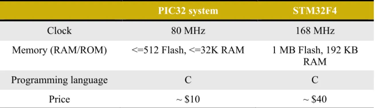
PIC32 system STM32F4
Clock 80 MHz 168 MHz
Memory (RAM/ROM) <=512 Flash, <=32K RAM 1 MB Flash, 192 KB
RAM
Programming language C C
Price ~ $10 ~ $40
Table 2.1 Comparison between PIC32 system and STM32F4 system. The STM32F4 system can support significant higher CPU clock frequency and RAM/ROM.
My early instrument designs have used the MCS51, MCS96, or PIC16/32 chips.
for data collection, storage and printing purposes. However, their disadvantages are: (1) low
CPU frequency, (2) low memory, and (3) incapable of scaling.
The early versions of our tactical stimulators used PIC32 chips, but we now use the
STM32 series chips to upgrade the system (Table 2.1).
2.3 STM32F4 Discovery Board
2.3.1 Introduction of STM32F4
STMicroelectronics (STMicroelectronics) Group was founded in June 1987 as a
merge between the Italian SGS Thomson Microelectronics and French semiconductor
companies. Since 1999, ST has been one of the worlds top ten semiconductor companies.
STM32 is a family of 32-bit microcontroller integrated circuits by STMicroelectronics.
The STM32 family consists of seven series of microcontrollers: F4, F3, F2, F1, F0,
L1, L0, and W. Each STM32 microcontroller series is based upon a Cortex-M4F, Cortex-M3,
M0 +, or M0 ARM processor core. The M4F is conceptually a
Cortex-M3 plus DSP and single-precision floating-point instructions. The STCortex-M32 F4-series is the
first group of STM32 microcontrollers based on the ARM Cortex-M4F core. It was released
in September 2011.
The summary for this series is:
♦ Core: ARM Cortex-M4F core works at a maximum clock rate of 180 MHz.
♦ Memory: Static RAM consists of up to 192 KB.
♦ Oscillators: consists of internal (16 MHz, 32 kHz), external (4 to 26 MHz, 32 to 1000
kHz).
2.3.2 STM32F4 Discovery Board
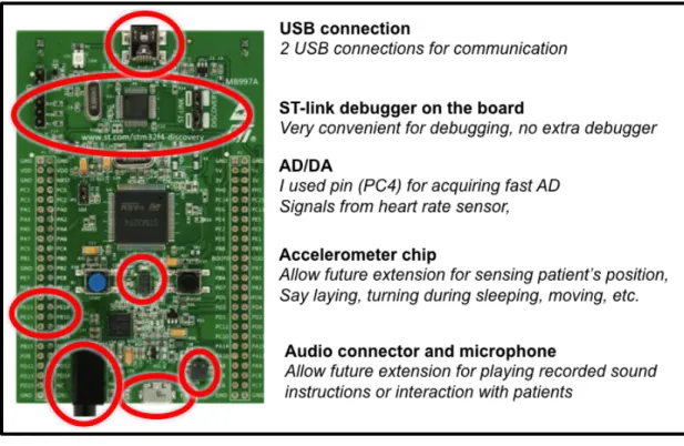
The STM32F4 discovery board has the following features (Figure 2.1):
• STM32F407VGT6 microcontroller featuring 32-bit ARM Cortex-M4F core, 1 MB
Flash, 192 KB RAM in an LQFP100 package;
• On-board LINK/V2 with selection mode switch to use the kit as a standalone
ST-LINK/V2 (with SWD connector for programming and debugging);
• Board power supply: through USB bus or from an external 5 V supply voltage;
• External application power supply: 3 V and 5 V;
• LIS302DL or LIS3DSH ST MEMS 3-axis accelerometer;
• MP45DT02, ST MEMS audio sensor, omni-directional digital microphone;
• CS43L22, audio DAC with integrated class D speaker driver;
• Eight LEDs:
• LD1 (red / green) for USB communication;
• LD2 (red) for 3.3 V power on;
• Four user LEDs, LD3 (orange), LD4 (green), LD5 (red) and LD6 (blue);
• 2 USB OTG LEDs LD7 (green) and LD8 (red);
• Two push buttons (user and reset);
• USB OTG FS with micro-AB connector;
• Extension header for all LQFP100 I / Os for quick connection to the prototyping
Figure 2.1 Display of The STM32F4 discovery board. From upper to lower, the important components/functions of this discovery board are marked with a red circle. It contains two USB connections a ST-link debugger for direct debugging an accelerometer chip for position sensing to allow for recording patients’ movements, and an audio connector and microphone to allow for further application of verbal instructions and sound recording.
2.3.3 Software Development Environments
We used the GCC + Eclipse as the software development environment.
Eclipse is an integrated development environment (IDE). It contains a base
workspace and an extensible plug-in system for customizing the environment. Eclipse is a
free and open source software that can be used to develop applications in different
programming languages. Eclipse CDT for C / C + + was used for our purposes.
The GNU Compiler Collection (GCC) (originally GNU C Compiler) was used. This
languages. It is also a free and open source software, it supplies useful tool kits for
developers, and it supplies free examples.
We selected Eclipse and GCC because they are open source and free software. Here I
listed some other alternative development workbench / compilers that can be selected from.
• TrueSTUDIO (~$4000 or a 32Kb limited Flash version for free),
• Cross Works (~$150),
• RKit (~$120 or Limit to 32kb for debugging),
• IAR (Complete tool kit with many integrated samples and solutions; costs thousands
of dollars, but there are two free versions: a 30 day trial version or a 32kb limited
flash version),
• MDK-ARM tool kit (Complete tool kit with many integrated samples and solutions;
costs thousands of dollars but there is a free 32kb light version),
CHAPTER 3
Heart Rate Detection
3.1 Introduction of the Pulse Sensor
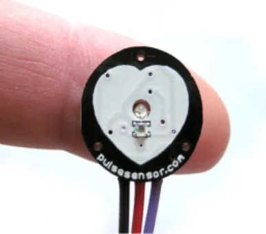
Considering the aspects of both the price and the size of different heart rate sensors,
our team decided to use the Pulse Sensor created by Joel Murphy and Yury Gitmanvanme as
the heart rate sensor for our new tactile system.
Figure 3.1 Appearance of the Pulse Sensor. Figure comes from the official website of the pulse sensor : http://pulsesensor.com/.
This sensor is approximately 1.58 cm in diameter, 0.32 cm thick, and costs around
$25 (Figure 3.1). The small, round shape of the Pulse Sensor makes it convenient for
obtaining the heart rate signal from subjects’ fingers, This fits well with our tactile system
since the system has been ergonomic designed for testing fingers. This Pulse Sensor is
relatively energy efficient, using 3V to 5V with a consumption of around 4mA at 5V, which
The Pulse Sensor uses photoplethysomgraph (PPG) technology to output the
heartbeat signal. With every heartbeat, there is a blood volume change inside all of the
arteries and capillaries. This change in volume influences the pressure of the blood vessel
wall, causing a change in the size of the blood vessel diameter. This change in the
morphology of the blood vessels affects light reflection, refraction and absorption. By
illuminating the skin with light and measuring the light reflected or transmitted, the repeated
blood volume change caused by the heartbeat can be detected. [12]
This Pulse Sensor uses a green LED (Kingbright; AM2520ZGC09) to illuminate the
subject’s fingertip, and a light sensor (Avago; APDS-9008) measures the amount of light that
bounces back from the fingertips. By checking the datasheet of AM2520ZGC09 and
APDS-9008, since the green LED produces light around 500 nm and the light sensor is extremely
sensitive to detecting light of the same wavelength, the light producer and sensor are
perfectly matched, allowing them to work together to effectively measure heartbeat
waveforms.
This Pulse Sensor also includes a filter chip (MCP6001) and an amplifier signal. The
filter chip helps to reduce the signal to noise ratio, allowing for easier and more accurate
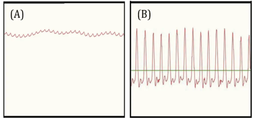
analysis (Figure 3.2).
3.2 Working Condition of the Pulse Sensor
We first used an oscilloscope to test the basic working conditions of the Pulse Sensor
in order to fully understand these conditions and to allow us to use it more efficiently. Based
on tests from the same subject, the Pulse Sensor produces a base signal comes 2.2 V.
Heartbeats produce 0.1 V variations on this base signal, appearing as small peaks. However,
during different tests on the same subject, we found that it is not easy to get clean signal as
shown in figure 3.2(B). Sometimes, the output signal includes fluctuations of unknown
origin, and the heartbeats’ wave intensity is too small to be detected. With practice, we
found that the signal’s stability could be significantly affected by three factors.
First, how tight the finger is bound to the Pulse Sensor greatly affects the intensity of
the heartbeat wave. If it is too tight or too loose, it will create an undetectable heart pulse,
while a proper tightness will help to optimize heartbeat signal intensity to 0.1V. We
hypothesize that the artery morphology and blood flow can be affected by how tight the
finger is bound, causing a change in the reflection light intensity. Adjusting the tightness of
the Pulse Sensor before each experiment is essential since an improper setup may result in
the heartbeat being too small to record, inducing an error in the calculation of the heart beat
The second factor is the movement of the finger attached to the Pulse Sensor. Even
small movements of the finger can induce extremely large fluctuation in the signal. The
movement of the finger may change the sensors relative position to the blood vessels and/or
induce change in ambient light, such as light leakage. Signal fluctuations caused by finger
movements would likely be interpreted by software as heartbeats, thus inducing error in the
recording and calculation of heartbeat intervals.
The third factor is the ambient illumination. The ambient lights have a very broad
wavelength (including wavelengths at 500-600nm) and are strong in light intensity. Leakage
of ambient light or a large change in the ambient illumination conditions can impede the
Pulse Sensor’s ability to detect small changes in light induced by pulse since the PPG signal
from the pulse is much smaller than that from the ambient light. Therefore, it is important to
decrease the receivable ambient light to a minimum by, for example, using a black band to
cover the sensor in order to increase the accuracy of heartbeat detection.
In order to get relatively stable signal from the pulse sensor, the following working
requirements must be satisfied when testing:
(1) Keep the finger touching the sensor, but not too tightly.
(2) Do not make any abrupt movements with the testing finger.
(3) Use black tape or similar material to cover the Pulse Sensor in order to reduce
3.3 Signal Processing and Analysis
3.3.1 Introduction of Heartbeat Signal
The goal of our signal processing and analysis is to document instantaneous
heartbeats and to calculate the time interval between two adjacent heartbeats.
As discussed above, under ideal conditions with tests from one subject, the signal
come out from the pulse sensor, has a base signal around 2.2 V, and small waves around
0.1V are induced by heartbeats.
The wave signal induced by heartbeats has a basic shape shown in Figure 3.3.
According to every heartbeat, the signal rises rapidly and then falls back to baseline. As is
shown in figure 3.3, heartbeat signal is repeating and predictable. There is one dominating
wave peak as well as some additional small peaks for each heartbeat.
3.3.2 Challenges and Solutions for Heartbeat Signal Processing
One direct way to process the signal is to find signal peaks, and then calculate time
intervals between adjacent peaks. The advantage of this method is that it is easy to use
software to recognize signal peaks by comparing signal values. If the signal value of one
point is larger than adjacent signal points both before and after, then it could be treated as a
peak. However, this method could cause misreading of heartbeats because of the complexity
of the signal. As shown in Figure 3.3, each heartbeat wave consists of a large and a small
peak. In addition, background noise could produce peaks as well.
Another idea of signal processing is using threshold to recognize heartbeats. When
the signal’s value is larger than a given threshold, a heartbeat wave begins and continues
until the signal’s value goes back below the threshold. The advantage of setting a threshold is
that it could prevent mislabeling of fluctuations that are of smaller amplitude compared to the
amplitude of a true heartbeat wave. These fluctuations with smaller amplitudes are normally
either background noise or local peaks of the complicated heartbeat waves.
Setting a proper threshold is of utmost importance in order to accurately recognize
heartbeat waves. However, the proper threshold should not be a constant value. This heart
rate module has been build up for testing different people, and different individuals may have
different finger conditions and even different blood volume change with each heartbeat.
Therefore, the signal intensity produced by heartbeats may be different for different people.
Second, as discussed above, a proper binding tightness can help optimize the signal intensity.
The tightness of finger binding to the Pulse Sensor is strongly related to the amplitude of
Sensor with exactly the same level of tightness in different experiments. Therefore, the signal
intensity produced by heartbeats may be different for different experiments and the threshold
for identifying heartbeats from the signal with different amplitudes should be different. A
proper threshold should be a dynamic value, which will change according to the amplitude of
heartbeat waves.
A proper threshold should also be sensitive to the amplitude of a heartbeat wave. As
discussed above, heartbeat waves are small fluctuations on the base signal. The amplitude of
heartbeat waves is much smaller than the base signal. In order to recognize the small
heartbeat waves, setting the threshold at a value that lies between the bottom and the peak of
the heart beat wave is ideal. Considering that the amplitude of a heartbeat wave may change
in different tests because of the tightness of binding or using a different test subject, a value
that could track the heartbeat wave amplitude would be a solution for a setting threshold [13].
In our experiment, a dynamic threshold that could track the heartbeat wave amplitude
is calculated through the function (1). This solution is suggested by the Pulse Sensor
inventors on their website
(http://pulsesensor.myshopify.com/pages/pulse-sensor-amped-arduino-v1dot1) and reviewed in [13]. The threshold for detecting the next heartbeat wave is
determined by the amplitude of previous heartbeat waves. The value is set by the following
function:
Dynamic Threshold = Minim + ½ * (Maximum – Minim) (1)
Where Minim is the bottom value of the previous heartbeat wave, and Maximum is
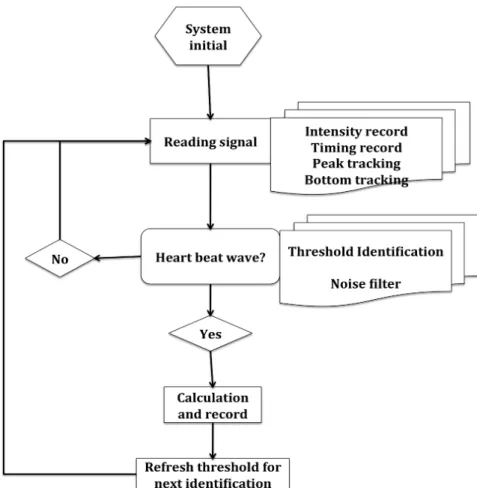
3.3.3 Diagram of Signal Processing
A diagram of our signal processing system is shown in Figure 3.4. This is based on
the signal processing method suggested by the Pulse Sensor inventors and [13].
Before any signal can be processed, analog signal must be converted to digital signal
for software analysis. The Stm32F4 Discovery Board completes this task by using an analog
to digital convertor (ADC). Detailed settings of the ADC will be discussed in Chapter Four.
An ADC sampling rate of 200 Hz was selected for our heart rate module, meaning that every
second, 200 data points are read into the system. Given that a normal, resting heart rate is
around 1 beat per second, frequency provides a good balance of data set size and accuracy of
the signal.
As is shown in the diagram, the first step is system initialization. All system settings
and thresholds for signal processing are set at default values at this point.
The second step is to read signal values. 200 points per second are read into system
for analysis. For each signal point, both intensity and timing values are saved in the signal
Figure 3.4 Diagram of the signal-processing program.
The next step is to identify whether or not a heartbeat is coming by comparing the
intensity of each signal point with a threshold. A dynamic threshold is used here as discussed
previously. If the intensity of a signal point is larger than the dynamic threshold, we believe a
heartbeat is coming, or the heartbeat is “on.” If the intensity is lower than the dynamic
threshold, we conclude that the heartbeat is “off.”
In addition to the dynamic threshold, other constant thresholds are used to filter out
signal noises. One smaller threshold is set to filter out small signal fluctuation caused by the
background noise, which has smaller amplitude than a normal heartbeat wave. One time
movement. These thresholds are also suggested by the Pulse Sensor inventors on the website:
http://pulsesensor.myshopify.com/pages/pulse-sensor-amped-arduino-v1dot1 .
If the software finds that the heartbeat is off, it goes back to the second step to read
values of signal points.
If the heartbeat is on, the software will save both the timing value when the heartbeat
starts and the time value when it ends. Also, the software will calculate the time interval
between the current heartbeat and previous heartbeat, as well as the current heart rate. In
addition, the software will refresh the dynamic threshold based on the amplitude of the
current heartbeat in order to identify the next heartbeat. At the end, the software will return to
CHAPTER 4
The Integration of Pulse Sensor to the CM5 System
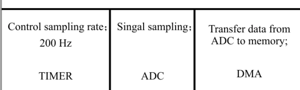
4.1 Required Settings for Stm32f4 for Pulse Sensor
As discussed in Chapter Two, the new generation of the tactile stimulator makes use
of an Stm32F4 Discovery Board. This chapter will discuss how to set up Stm32F4 Discovery
Board properly so that it can automatically collect heartbeat data from a Pulse Sensor.
In order to properly read a heartbeat signal from a Pulse Sensor and transfer the data
to the software for signal processing, special settings are required for three resources on the
Stm32F4 Discovery Board. The three resources are Timer, ADC and DMA (Table 4.1).
Table 4.1 Three resources used for reading heartbeat signal.
As discussed in Chapter Three, a frequency of 200Hz is adopted for sampling the
signal, but this frequency is quite low compared to the system clock of STM32F4 Discovery
micro-controller reads heartbeat signals from the Pulse Sensor
Control sampling rate;
200 Hz
TIMER
Singal sampling;
ADC
Transfer data from ADC to memory;
Board, which is set at 168MHz. Therefore, a Timer is required to output a 200Hz clock that
will trigger the ADC working at sampling rate of 200Hz.
In order to transfer the data converted by an ADC to the place where it will be
analyzed for heart rate information, Direct Memory Access (DMA) request is used to
complete this task efficiently. DMA can access memory to transfer data without affecting
the process of the microcontroller. A designer will sometimes encounter the problem that
several DMA requests will interfere with each other. Thus, we needed to confirm that the
DMA request for the heart rate module is not conflicting with other DMA requests. We also
set an interrupt handler for this DMA request. Therefore, after each DMA transfer of data,
the interrupt handler will activate a software program to analyze the data.
In summary, the setting on an STM32F4 Discovery Board for a Pulse Sensor includes
three requirements: a Timer, an unused ADC, and a separate DMA request.
4.2 Conflicts on Using Recourses
There are three A/D convertors included in the stm32f4 system (Figure 4.1). ADC1 is
a master, while ADC2 and ADC3 are slaves. They can either work independently in
“Independent Mode,” in which ADC2 and ADC3 will automatically have the same sampling
rate and DMA transfer request as ADC1 automatically, or they can work dependently in
“Multi-ADC Mode,” in which all three ADCs will have separate sampling rates and separate
DMA transfer requests (data sheet).
ADC1 and ADC2 have already been used for the other functional modules in our
(20KHz) and they share the same DMA transfer request. Specifically, ADC1 works as the
master and ADC2 works as the slave. ADC2 will begin sampling data automatically with
ADC1’s action of sampling, and the data sampled by both ADC1 and ADC2 will be mixed
together by using the same DMA transfer request.
Figure 4.1 Multi ADC block diagram. Figure comes from the Data sheet of STM32F4 Discovery Board.
ADC3 is the only unused ADC in the CM system; therefore it is the only choice for
the heart rate module. However, setting the ADC3 parameters is a challenging task. If we do
not change any other modules, ADC3 will work dependently with ADC1 and ADC2 with the
would also share the same DMA request with ADC1 and ADC2, meaning that all the data for
the heart rate module would mix with the data from the other modules. There are two
challenges faced if using this method: (1) how to find the right data for the heart rate among
the mixed data, and (2) How to deal with the much bigger space requirement of the data.
Another choice is to change the mode of ADC1 and ADC2 and let all three ADCs
work independently. This solves the problem of setting the ADC3 for in the heart rate
module. The challenge here is how to make sure that ADC1 and ADC2 continue to work in
the same way as before with (1) ADC1 and ADC2 working simultaneously at the same
sampling rate of 20KHz, and (2) the DMA request to transfer data to the same place is
unaffected for ADC1 and ADC2.
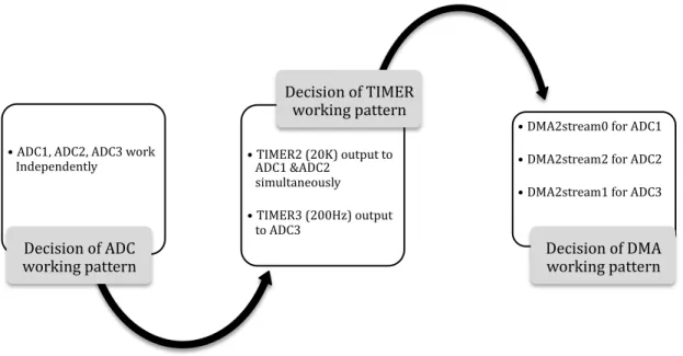
4.3 Solution of Settings for the Integration
As discussed above, having the three ADCs working dependently and independently
would both cause challenges. If all three ADCs worked dependently, the complexity of the
software would necessarily increase in order to find the right data of each module from all
the data mixed together. Therefore, the solution of making all ADCs work independently is
choosing in our system.
The final solution for the ADC settings, Timer setting, and DMA settings is shown in
Figure 4.2 A schematic figure showing the working pattern for ADC, Timer and DMA.
Here, ADC1, ADC2 and ADC3 all work independently. Setting the ADCs include the
following steps:
• Step one: Set ADCs to work at independent mode.
• Step two: Enable external event triggering so ADC sampling can be triggered by the
Timers output; Disable continuous sampling module and scan sampling mode.
• Step three: Enable DMA request for each ADC, so that data from ADCs can be
transferred.
• Step four: Set the resolution for sampling. Resolution for ADCs is set at 12bits in our
system.
Two Timers are chosen in this solution for our system. One Timer outputs a clock of
20KHz to ADC1 and ADC2 for other modules. The other Timer outputs a clock of 200Hz to
ADC3 for the heart rate module. There are fourteen Timers built in the system including
advance-control Timers, general-purpose Timers and basic Timers, and there are different
channels for each timer (check the data sheet of the microcontroller). Two general-purpose
• ADC1, ADC2, ADC3 work Independently
Decision of ADC working pattern
• TIMER2 (20K) output to ADC1 &ADC2
simultaneously • TIMER3 (200Hz) output
to ADC3
Decision of TIMER working pattern
• DMA2stream0 for ADC1
• DMA2stream2 for ADC2
• DMA2stream1 for ADC3
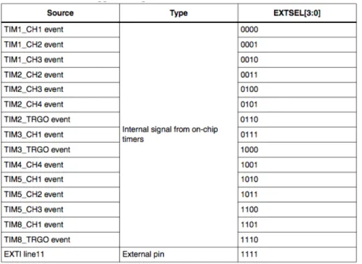
Timers are sufficient for the purpose of outputting two different clocks. There are thirty
Timer events that can trigger ADC conversions. Table 4.2 shows fifteen possible Timer
events that can trigger normal ADC conversions. TIM2-CH2, Channel2 of general-purpose
Timer2, is selected for triggering both ADC1 and ADC2and TIM3-CH1, Channel 1 of
general-purpose Timer3, is selected for triggering ADC3.
Table 4.2 List of fifteen possible Timer events that could trigger normal ADC conversions. This table comes from the Data sheet of STM32F4 Discovery Board.
Basic settings for Timer2 and Timer3 are as follows:
• Step one: Set Timers working mode. Both Timer2 and Timer3 work at output Pulse
Width Modulation mode (PWM mode). This mode allows the timer to generate a
signal with a frequency determined by a value stored in registers.
• Step two: Set a prescaler. The prescaler is used to obtain a timer clock by dividing the
system clock by any factor between 1 and 65536. The prescaler is set at 83 for
function (2), we get a 2MHz timer clock for Timer 2 and a 20KHz timer clock for
Timer3.
Timer clock = System clock / (Prescaler + 1) (2)
• Step three: Set a counter period. Based on the counter period value, the Timer
generates a counter overflow event. Counter period for both Timer2 and Timer3 is set
at 99. Based on function (3), we get a 20KHz PWM from Timer2 and a 200Hz PWM
from Timer3.
PWM frequency = Timer clock/(Counter period +1) (3)
Table 4.3 List of different DMA2 request mapping. This table comes from the Data sheet of Stm32F4 Discovery Board.
Three different DMA request streams are used in this solution. In all, there are two
DMA controllers (DMA1 and DMA2) built in the micro controller. Each DMA controller has
eight streams, and each stream has up to 8 channels (check the data sheet of the
Finally, channel 0 of stream 0 is chosen for ADC1, channel 1 of stream 2 is chosen for
ADC2, and channel 2 of stream 1 is chosen for ADC3. .
Basic settings for DMA transfer are as following:
• Step one: Set data transport parameters: transport direction, data address and data
size.
• Step two: Set the priority for the three DMA requests. The four priority levels are
very high, high, medium, low. All three DMA requests are set at high priority in our
system.
• Step three: Set DMA interrupt handlers for each ADC. In our system, when a DMA
transfer of ADC data completes, a DMA interrupt handler will be executed. In DMA
interrupt handlers, messages are set in order to make the corresponding software
program in queue for the next execution. For example, after the DMA transfer of data
from ADC3 is completed, a DMA interrupt handler will put a signal-processing
program in queue for execution. This signal-processing program is used to analyze
CHAPTER 5
Communication and Display of Detected Heart Rate Characteristics
5.1 Data for Communication and Displaying
As discussed in chapters 3 and 4, the stm32f4 discovery board is set to sample signal
from the Pulse Sensor, and a signal-processing program is used to identify heartbeats from
the sampled signal. After reading and analyzing heart rate signals, the next step of the heart
rate module is to transfer the heart rate characteristics to a computer for storage and display.
The heart rate module prepares two heart rate characteristics for communication and
display on computers, as shown on the right side of figure 5.1. These characteristics are heart
beat interval and current heart rate, both of which are half-word variables (16 bits). The
former is saved circularly, and our system is designed to save up to 250 in total.
Figure 5.1 briefly describes how to obtain the two heart rate characteristics. Each
second, 200 signal data points are read into system for processing. Each data point has a one
half-word intensity value and a one half-word timing value, and each heartbeat contains one
half-word start value and one half-word end time value. The signal-processing program
identifies the heartbeats, and timing values of each heartbeat are recorded. Heart beat
intervals of adjacent beats are calculated by subtracting the start time of adjacent beats, with
Where n is a positive integer and units are in beats/min. In our system, n is set at 5 for
calculating heart rate based on 5 continuous heartbeats.
Figure 5.1 A schematic flow chart showing how to obtain the two heart rate characteristics.
As the signal-processing program continues to identify new heartbeats, corresponding
new heart beat intervals and current heart rate will be calculated and saved. After reaching
the maximum of 250 saved heart beat intervals, the oldest intervals will be replaced in the
memory sequentially with the new intervals.
5.2 USB Communication of Data and Display of Heart Rate Characteristics
5.2.1 USB Communication for the New Tactile Stimulator
USB communication has already been developed and used for other modules of the
tactile stimulator by our team in Dr. Mark Tommerdahl’s lab. As shown in figure 5.2, the
computer has a special database for saving collected research data. And a specific web
protocols designed by researcher. USB communication of data between the CM system and
the computer is controlled by the web application software.
Figure 5.2 The USB communication between tactile stimulator and a computer.
5.2.2 USB package of heart rate module
In order to communicate data for the heart rate module, a heart rate package is
designed, as shown in Table 5.1.
64 Bytes/Heart rate Package
Command: 1 Byte Subcommand: 1 Byte Current Heart Rate: 1 Half-‐word Extra data: 8 Bytes Index of Heart Beat Intervals: 1 Byte Length of Heart Beat Intervals: 1 Byte
The package has a total size of 64 bytes, including 1 byte command, 1 byte
subcommand, 1 half-word current heart rate value, 8 bytes extra data, 1 byte address index of
heart beat intervals, 1 byte length heart beat intervals, and 25 half-words heart beat intervals.
5.2.3 Controls of USB communication for the heart rate module
The tactile stimulator and the computer use one byte command to identify heart rate
packages and use one byte subcommand to make different controls on the communication of
heart rate packages.
Figure 5.3 Control of heart rate module by the subcommand of USB communication.
Four controls of communication are programmed for the heart rate packages, as is
shown in Figure 5.3. When subcommand equals 1, USB communication works at the mode
1, in which current heart rate and the latest 25 heart beat intervals will be transferred to the
computer. If the subcommand is 2, USB communication will work in mode 2, and the current
heart rate and 25 heart beat intervals will be transferred from any address designated by the
computer. When the tactile system receives a subcommand equaling to 3, the heart rate
module will restart and the system will clear old saved data, start detecting heartbeats, subcommand
= 1 Transfer data at mode 1
Subcommand =
2 Transfer data at mode 2
Subcommand =
3 Restart heart rate module
Subcommand =
calculating heart rate characteristics, and save the data in the memory. When the tactile
system receives a subcommand equaling to 4, the heart rate module will stop saving the new
calculated heart beat intervals to the memory, while the current heart rate will still be
updated.
By setting the subcommand at four different values, researchers on the computer side
are now able to control the transferring of detected heart rate characteristics.
5.2.4 Display of the Heart Rate Data
These transferred heart rate data will finally be added to the database on the computer
for further study. However displaying these data will greatly help the heart rate testing
experiment. Displaying transferred heart rate data could help to check if the heart rate
module has been built correctly.
During the development of this heart rate module, three different methods have been
used to display the heart rate data, as shown in Table 5.2.
Display of heart rate characters
Display heartbeats using LED
GPIO writing based on timing values of each
Heartbeat
Display on Terminal by USB communication
Current Heart rate &
Heart Beat Intervals
Display on web application by USB
communication
The first way is using LED to display detected heartbeats. As discussed above, a
signal-processing program is used to identify heartbeats from sampled signal, and both the
starting time point and ending time point of each heartbeat will be identified. When the start
time of a heartbeat is identified, the system turns on the LED by outputting a high voltage to
it. When the ending time of the heartbeat is identified, the system turns off the LED by
outputting a low voltage to it. In this way, the LED flashes according to the subject’s
heartbeat.
The second way is to display heart rate characteristics on the terminal of a computer.
After building up the USB communication for the heart rate module, it is able to display the
transferred data on the terminal. Figure 5.4 shows an example of terminal display of
transferred heart rate data.
The top graph of figure 5.4 shows data transferred at mode 1. The bottom graph
shows that the heart rate module is stopped from saving new heart beat intervals, and data is
transferred at mode 2. Rectangles in different colors mark the current heart rate, transferred
heart rate intervals, and the number of heart beat intervals that have been saved by the
Figure 5.4 Display detected heart rate character on the terminal. Rectangles in different color mark out the Current Heart Rate, transferred Heart Beat Intervals, and the number of Hear Beat Intervals, respectively.
The third way is to display the current heart rate on a web application. While running
experiments, a web application with a user-friendly interface is running on the computer.
Displaying the current heart rate value on the user interface is a convenient way to provide
real time heart rate information to both researchers and test subjects.
Displaying real time heart rate on the user interface could be realized by setting a
regular program to (a) read the current heart rate value periodically from the heart rate
module, and (b) update the heart rate value being displayed on the user interface. Figure 5.5
Figure 5.5 Display of real time heart rate on the web application.
During the process of building the heart rate module, displaying heart rate
characteristics has become a convenient and practical way to check the accuracy of signal
processing. By testing different subjects, the signal-processing program built in the heart rate
CHAPTER 6
Conclusion
We report that our team has successfully developed a new generation of Cortical
Metrics systems (CM), using the STM32F4 Discovery Board with an added heart rate
measurement function into the system. In this thesis, I introduced the background of this
project, the hardware system “STM32F4 Discovery Board”, and the compiling
environmental settings I used for this system. I tested and discussed the proper working
conditions of the heart rate sensor and used signal-processing methods to identify heartbeats
from the signal coming out from the Pulse Sensor. I demonstrated how to reasonably arrange
the resources on the system board so that different modules of the tactile system can provide
different functions independently and effectively. We successfully integrated the heart rate
module into the new tactile stimulator system. We also worked on the communication and
display of detected heart rate and used three different displaying methods for the heart rate
module (one on board, and two on computer).
The new CM system with heart rate measurement capability has already been
successfully tested and used by multiple users, from Kids to Navy soldiers. The system is
patients and autism patients. The heart rate variation may supply us with new information
during the test.
We are also considering adding other modules into the new CM system, because of
its scalable abilities, such as: voice instruction function and blue tooth function.
In summary, we developed the new generation of Cortical Metrics systems (CM) with
heart rate measurement function, the actual tests showing this system is very stable and
reliable. We are looking for more researchers who can use and apply this system to their
REFERENCE
[1] J. K. Holden, R. H. Nguyen, E. M. Francisco, Z. Zhang, R. G. Dennis, and M. Tommerdahl, “A novel device for the study of somatosensory information processing,”
J. Neurosci. Methods, vol. 204, no. 2, pp. 215–220, Mar. 2012.
[2] V. Tannan, R. Dennis, and M. Tommerdahl, “A novel device for delivering two-site vibrotactile stimuli to the skin,” J. Neurosci. Methods, vol. 147, no. 2, pp. 75–81, Sep. 2005.
[3] V. Tannan, R. G. Dennis, Z. Zhang, and M. Tommerdahl, “A portable tactile sensory diagnostic device,” J. Neurosci. Methods, vol. 164, no. 1, pp. 131–138, Aug. 2007.
[4] M. Tommerdahl, V. Tannan, C. J. Cascio, G. T. Baranek, and B. L. Whitsel, “Vibrotactile adaptation fails to enhance spatial localization in adults with autism,”
Brain Res., vol. 1154, pp. 116–123, Jun. 2007.
[5] M. Tommerdahl, V. Tannan, J. K. Holden, and G. T. Baranek, “Absence of stimulus-driven synchronization effects on sensory perception in autism: Evidence for local underconnectivity?,” Behav. Brain Funct., vol. 4, no. 1, p. 19, Apr. 2008.
[6] Z. Zhang, V. Tannan, J. K. Holden, R. G. Dennis, and M. Tommerdahl, “A quantitative method for determining spatial discriminative capacity,” Biomed. Eng. OnLine, vol. 7, no. 1, p. 12, Mar. 2008.
[7] R. H. Nguyen, C. Gillen, J. C. Garbutt, A. Kampov-Polevoi, J. K. Holden, E. M. Francisco, and M. Tommerdahl, “Centrally-mediated sensory information processing is impacted with increased alcohol consumption in college-aged individuals,” Brain Res., vol. 1492, pp. 53–62, Jan. 2013.
[8] M. Malik, J. T. Bigger, A. J. Camm, R. E. Kleiger, A. Malliani, A. J. Moss, and P. J. Schwartz, “Heart rate variability Standards of measurement, physiological interpretation, and clinical use,” Eur. Heart J., vol. 17, no. 3, pp. 354–381, Mar. 1996.
[9] I. Cygankiewicz and W. Zareba, “Chapter 31 - Heart rate variability,” in Handbook of Clinical Neurology, vol. Volume 117, Ruud M. Buijs and Dick F. Swaab, Ed. Elsevier, 2013, pp. 379–393.
[10] P. Marwedel, Embedded System Design: Embedded Systems Foundations of
Cyber-Physical Systems, 2nd ed. 2011 edition. Dordrecht: Springer, 2010.
[12] J. Allen, “Photoplethysmography and its application in clinical physiological measurement,” Physiol. Meas., vol. 28, no. 3, pp. R1–R39, Mar. 2007.