Cadence SiP Technology
Manufacturers of high-performance consumer electronics are turning to SiP design because it offers a number of significant advantages such as increased functional density, integration of disparate chip technol-ogies, low power, improved signal performance/integrity, and ease of integration into a PCB system. However, SiP design also requires expert engineering talent in widely divergent fields, which historically has limited mainstream adoption. By streamlining the integration of multiple high-pin-count chips onto a single substrate through a connec-tivity-driven methodology (Figure 1), Cadence SiP co-design technology allows companies to adopt what were once expert engineering SiP design capabilities for mainstream product development. Cadence SiP solutions seamlessly integrate with Cadence Innovus™ technology for chip/package interconnect refinement and Cadence Virtuoso® technology for
schematic-driven analog/mixed-signal module design.
Connectivity-Driven SiP
The Cadence connectivity-driven SiP flow is tuned for integrating multiple large high-pin-count chips onto a single substrate. This flow targets the major challenges of SiP-level connec-tivity definition and management— physical concept prototyping of the SiP floorplan, including multi-chip die stacks, interposers, substrate cavities, and die bump matrix refinement— to optimize and minimize substrateconnectivity routing and signal integrity challenges. The SiP flow is built around a unique System Connectivity Manager that forms part of the SiP Digital Architect product. Cadence technology for complete SiP implementation, including IC padring/ bump array refinement and detailed package-level signal integrity analysis
System-in-package (SiP) implementation presents new hurdles for system architects and designers.
Conventional EDA solutions have failed to automate the design processes required for efficient
SiP development. By enabling and integrating design concept exploration, capture, construction,
optimization, and validation of complex multi-chip and discrete substrate assemblies on PCBs,
Cadence
®SiP design technology streamlines the integration of multiple high-pin-count chips onto
a single substrate.
Connectivity-driven implementation and optimization of single-
or multi-chip SiPs
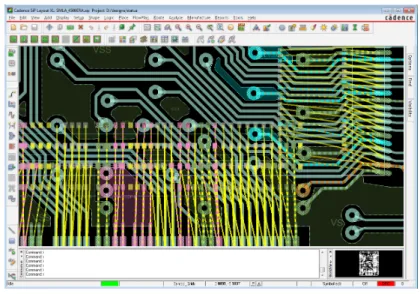
Figure 1: Complex multi-chip SiP designs, including wirebond and flipchip attach die, are easily and quickly constructed in this powerful rules- and constraint-driven environment
www.cadence.com 2 and extraction and 3D modeling, is
achieved through the use of the following four key product technologies:
• Cadence SiP Layout: Detailed constraint- and rules-driven physical substrate construction and manufacturing preparation. Includes die abstract refinement so the die bump-array is optimized to the BGA ballout. Changes to the die bump-array can be communicated through a distributed ECO process with Innovus and Virtuoso technologies.
• Cadence SiP Digital Architect: Front-end design definition of the logical connec-tivity across the multiple substrates that make up the SiP
• Cadence Virtuoso SiP Architect: Provides an analog/mixed-signal schematic and circuit simulation-driven SiP module design flow
• Cadence Allegro® Sigrity™ Package
Assessment and Extraction Option: Detailed interconnect extraction, 3D package modeling, and power-aware signal integrity analysis
SiP Layout
Cadence SiP Layout provides a constraint- and rules-driven layout environment for SiP design. This includes substrate place and route, final connectivity optimization at the IC, substrate, and system levels, manufacturing preparation, full design validation, and tapeout. The environment features integrated IC/package I/O padring/bump array refinement and 3D die stack creation and editing capabil-ities. In addition, full online design-rule checking (DRC) supports the complex and unique requirements of all combina-tions of laminate, ceramic, and deposited substrate technologies. Multi-layer flip-chip along with radial any-angle routing provide rapid constraint-driven interconnect creation.
IC padring/bump array refinement
SiP Layout enables the package designer to refine/optimize the IC bump array in the context of the IC package BGA ball map and its associated breakout and routing through the use of a DIE Abstract, an open ASCII XML file that contains the IC’s
I/O padring, RDL, and bump array. The DIE Abstract can be created by the IC design tools (Innovus and Virtuoso solutions) or from Cadence OrbitIO™ Interconnect
Designer (Figure 2). Refinements made to the DIE Abstract during package design can be communicated back to the IC designer as an updated DIE Abstract and read directly by the Innovus and Virtuoso solutions.
Auto/interactive wirebonding
A highly productive environment provides fast, powerful, and flexible bondshell creation and editing. Constraint- and rules-driven automatic bondfinger array placement can be used with staggered die pads, multiple bond levels, multiple
bond rings, and both symmetrical and non-symmetrical designs. For fast initial what-if prototyping of single or multiple die stacks, the “autobond” feature instantly creates a symmetrical bondshell pattern, including power and ground rings. Unique push and shove bondfinger editing enables extremely complex bondshells to be developed in minutes, delivering unparalleled capability and productivity. True wireprofile support enables DFM-driven design using manufacturing-verified wire loop data (Figure 3). An included Kulicke and Soffa loop-profile library (Figure 4) ensures that any wirebond patterns designed meet K&S manufacturing signoff.
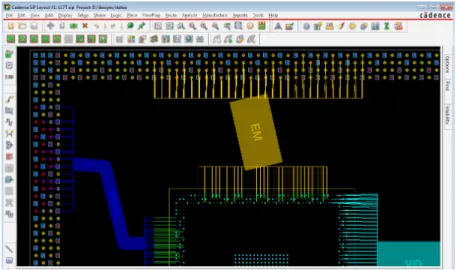
Wirebond-Figure 2: The IC Package designer imports the interconnect architecture from the OrbitIO Interconnect Designer as a series of pathways including breakouts.
attached die flags and power/ground rings can be quickly created, edited, and optimized for multiple voltage supplies.
3D Die Stack Editor
The Die Stack Editor (Figure 5) provides a 3D construction environment (Figure 6) for assembling complex die stacks that can include spacers, interposers, and die-attach methods such as wirebond and flip-chip.
3D Design Viewer
The Cadence 3D Design Viewer is a full solid-model 3D viewer and 3D wirebond DRC solution for complex IC package designs. It allows users to visualize and investigate an entire design, or a selected design subset such as a die stack or complex via array. It also provides a common reference point for cross-team design reviews.
ARC
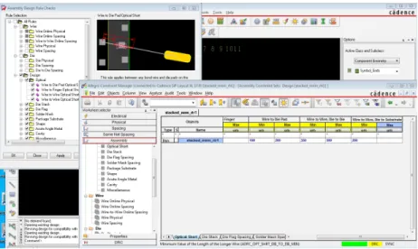
A comprehensive assembly (and manufac-turing) rule checker (ARC) provides more than 50 SiP-specific checks (Figure 7). Checks can be executed as a check-group, individually, or as a custom selection. Check results appear in the Constraint Manager DRC tab and as graphical markers in the design.
Benefits
• Provides 3D die stack creation/editing capabilities for rapid stack assembly and optimization
• Enables IC bump array refinement and connectivity optimization at IC, substrate, and system levels using IP-secure Die Abstracts
• Allows connectivity assignment and optimization between ICs and substrate for minimal layer usage based on signal integrity and routability
• Reduces tedious, time-consuming, and manual breakout editing via flip-chip die auto-route breakout
• Speeds implementation and reduces potential errors using constraint-driven HDI design with automation-assisted interactive routing
• Includes comprehensive substrate DFM capabilities for rapid manufacturing preparation
• Provides 3D design viewer and DRC for accurate full 3D wire bondshell verifi-cation, design review debug, and design documentation for assembly and test • Reduces design cycle time and optimizes
designer resources with team-based design partitioning
Embedded custom (user-defined) DRC checking
Integrated into SiP is an advanced-language rule-checking engine that can eliminate tedious traditional post-design manufacturing mask checking. This engine can substantially reduce time to manufac-turing readiness, streamlining the process and empowering the package designer.
Benefits
• Custom DRC rules can be written and encrypted using the optional rules developer toolkit
• Custom DRC errors are displayed graphically and shown in Constraint Manager
Figure 4: Includes a library of K&S-certified wire profiles optimized for their wirebonders.
Figure 6: 3D design viewer and 3D DRC
Figure 5: Complex stack-die construction including spacers and interposers is managed by
the Die Stack Editor
www.cadence.com 4
SiP Digital Architect
Cadence SiP Digital Architect provides an environment for early connectivity and constraint authoring and driven co-design methodology across die abstract(s), die stack, interposer, and package substrate. Its System Connectivity Manager (SCM) (Figure 8) manages any changes in logical connectivity or pin/ball signal assignments and provides the master logical definition for LVS.
Benefits
• Enables rapid system-level connectivity capture with the ability to bind into alternative physical implementation scenarios to evaluate performance and tradeoffs
Virtuoso SiP Architect
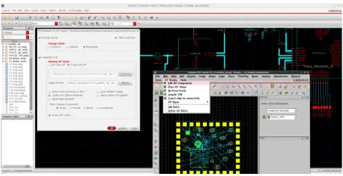
While SiP design makes it possible to combine mixed-signal and analog chips of disparate technology on the same substrate, it presents a number of challenges. These challenges include designing and integrating mixed-signal and analog chips with package substrate-level interconnect, as well as enabling top-level pre- and post-layout and signal integrity extraction technologies. Cadence Virtuoso SiP Architect provides a full-featured mixed-signal design flow and design exploration environment for multiple chip and discrete component integration (Figure 9). Working directly with the Virtuoso RF/analog chip design environment, Virtuoso SiP Architect provides full circuit simulation of multi-technology chips and the IC package substrate. It builds the package-level design as a simulation-capable schematic for hand-off to Cadence SiP Layout, and receives in return the substrate-level inter-connect models for post-route circuit simulation.Benefits
• Provides single schematic and circuit simulation representation of the IC(s) and the SiP package
• Integrates with Virtuoso Analog Design Environment
• Supports bi-directional ECO and LVS flow for full co-design implementation • Implements design from Virtuoso
output to package-level SiP schematic
• Automates circuit simulation testbench management
• Optimizes I/Os at the die bump level with a DIE abstract-based package-driven flow
Figure 8: The SCM enables the designer to rapidly construct SIP connectivity while managing cross-fabric signal name mapping and transitions.
Figure 9: The Virtuoso SiP Architect delivers a single circuit-simulation schematic-driven approach that encompasses multiple chips and the IC package.
Cadence Design Systems enables global electronic design innovation and plays an essential role in the creation of today’s electronics. Customers use Cadence software, hardware, IP, and expertise to design and verify today’s mobile, cloud, and connectivity applications. www.cadence.com
Allegro Sigrity Package
Assessment and Extraction
Option
The Cadence Allegro Sigrity Package Assessment and Extraction Option enables a package analysis and modeling solution that begins with early performance assessment, DC and AC PDN analysis, and moves to full-package extraction with hybrid solvers or detailed extraction of package segments with 3D full-wave solvers (Figure 10). The following Sigrity technologies are included with the Allegro Sigrity Package Assessment and Extraction Option to enable a complete solution for the assessment, analysis, and modeling of IC packages:
• A package assessment engine that allows quick detection of problematic package design practices, including detection of excessive inductive package pins, uncontrolled impedances, and high coupling
• A power-aware hybrid solver extraction engine, enabling RLGC and S-parameter model extraction of the complete coupled signal and PDN
• A full-wave 3D solver for high-frequency interconnect extraction of detailed structures within IC packages • IR-drop analysis, including
electrical-thermal co-simulation that considers both component and Joule heating, space dependent temperature distri-bution, and current density computation for planes, vias, and interconnect
Design flow
IC package performance assessment can begin at early stages of physical design, long before final package layout. Feasibility studies can be performed with initial connectivity to help determine which package type provides the best electrical performance for the lowest cost. For example, DC IR-drop and current constraint-driven stack-up options, as well as signaling topology tradeoffs, may be
explored and decided. As the package design continues, signal and PDN models can be extracted for comparison against RLC parasitic constraints and signals characterized for key attributes such as impedance and crosstalk or insertion and return losses. Thermal considerations may also be explored through the available coupled electro-thermal analysis capability. As the design reaches its final stages, full-package assessment (including IR-drop) and model extraction can be performed and an HTML signoff report generated to ensure that any significant problems are caught and the design fully documented. For packages expected to operate at high frequency, 3D full-wave extraction can be performed on critical package regions to ensure package performance specifica-tions are met.
Benefits
• Uses embedded hybrid solver for efficient RLGC or S-parameter extraction of full IC packages
• Implements 3D full-wave solver for detailed extraction of high-frequency structures
• Optimizes IR-drop signoff checking against power specifications
Cadence Services and Support
• Cadence application engineers cananswer your technical questions by telephone, email, or Internet—they can also provide technical assistance and custom training
• Cadence-certified instructors teach more than 70 courses and bring their real-world experience into the classroom
• More than 25 Internet Learning Series (iLS) online courses allow you the flexibility of training at your own computer via the Internet
• Cadence Online Support gives you 24x7 online access to a knowledgebase of the latest solutions, technical documen-tation, software downloads, and more.
Figure 10: Sigrity extraction and 3D modeling technology is directly integrated, enabling comprehensive rapid analysis and simulation model creation