28
Libra: Software-Controlled Cell Bit-Density to Balance Wear
in NAND Flash
XAVIER JIMENEZ, DAVID NOVO, and PAOLO IENNE, Ecole Polytechnique F´ed´erale de Lausanne (EPFL), School of Computer and Communication Sciences, CH–1015 Lausanne, Switzerland
Hybrid flash storages combine a smallSingle-Level Cell(SLC) partition with a largeMultilevel Cell(MLC) partition. Compared to MLC-only solutions, the SLC partition exploits fast and short local write updates, while the MLC part brings large capacity. On the whole, hybrid storage achieves a tangible performance improvement for a moderate extra cost. Yet, device lifetime is an important aspect often overlooked: in a hybrid system, a large ratio of writes may be directed to the small SLC partition, thus generating a local stress that could exhaust the SLC lifetime significantly sooner than the MLC partition’s. To address this issue, we proposeLibra, which builds on flash storage made solely of MLC flash and uses the memory devices in SLC mode when appropriate; that is, we exploit the fact that writing a single bit per cell in an MLC provides characteristics close to those of an ordinary SLC. In our scheme, the cell bit-density of a block can be decided dynamically by the flash controller, and the physical location of the SLC partition can now be moved around the whole device, balancing wear across it. This article provides a thorough analysis and characterization of the SLC mode for MLCs and gives evidence that the inherent flexibility provided byLibra simplifies considerably the stress balance on the device. Overall, our technique improves lifetime by up to one order of magnitude at no cost when compared to any hybrid storage that relies on a static SLC-MLC partitioning.
Categories and Subject Descriptors: B.3.2 [Design Styles]: Mass Storage; D.4.2 [Storage Management]: Allocation/Deallocation Strategies
General Terms: Design, Experimentation, Measurement, Performance, Reliability
Additional Key Words and Phrases: NAND flash memory, lifetime, endurance, SLC, MLC, wear leveling, wear balancing
ACM Reference Format:
Xavier Jimenez, David Novo, and Paolo Ienne. 2015. Libra: Software-controlled cell bit-density to balance wear in NAND flash. ACM Trans. Embedd. Comput. Syst. 14, 2, Article 28 (February 2015), 22 pages. DOI: http://dx.doi.org/10.1145/2638552
1. INTRODUCTION
NAND flash memory is the leading data storage technology for mobile devices, such as MP3 players, smartphones, tablets, and netbooks. It features low power consumption, high responsiveness, and mobility. However, flash technology also comes with its share of inconveniences. The device has a very specific physical organization, which results in a coarse granularity of data accesses. As with any EEPROM, memory cells need to be erased before being written again. Moreover, a flash memory cell can only be written a limited number of times before wearing out. The severity of these limitations Authors’ addresses: X. Jimenez, D. Novo, and P. Ienne, EPFL-IC-ISIM-LAP, Station 14, INF 137, 1015 Lausanne, Switzerland; emails: {xavier.jimenez, david.novo, paolo.ienne}@epfl.ch.
Permission to make digital or hard copies of part or all of this work for personal or classroom use is granted without fee provided that copies are not made or distributed for profit or commercial advantage and that copies show this notice on the first page or initial screen of a display along with the full citation. Copyrights for components of this work owned by others than ACM must be honored. Abstracting with credit is permitted. To copy otherwise, to republish, to post on servers, to redistribute to lists, or to use any component of this work in other works requires prior specific permission and/or a fee. Permissions may be requested from Publications Dept., ACM, Inc., 2 Penn Plaza, Suite 701, New York, NY 10121-0701 USA, fax+1 (212) 869-0481, or permissions@acm.org.
c
2015 ACM 1539-9087/2015/02-ART28 $15.00 DOI: http://dx.doi.org/10.1145/2638552
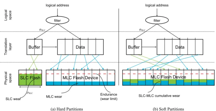
Fig. 1. Hard versus soft partitioning. A hybrid FTL redirects small writes to a page-level mapped buffer and directs large sequential writes directly to the data partition. The buffer is mapped to an SLC to benefit from low write latency and low energy, while the data uses an MLC for density. When writes are unbalanced across buffer and data, a hard partition will wear out faster than the other, while soft partitioning (the contribution of the present article) allows for balancing the wear on the global device.
is somehow mitigated by a software abstraction layer, calledFlash Translation Layer
(FTL), which interfaces between common file systems and the flash device.
The basic functionality of an FTL is the translation of logical addresses to physical addresses. Such translation can be done following various policies, which directly affect performance, lifetime, and device cost. Furthermore, the address translation table is typically stored in expensive RAM cells, generally SRAM or DRAM, which makes the table size a critical design parameter of any FTL. In particular, a small translation table is cheap but implies coarse-grained data manipulation (block level) that results in poor performance and lifetime. Instead, a large table enables fine-grained data manipulation (page level) and thus higher performance and lifetime, but at a significant increase in device cost.
Hybrid FTLs [Chiao and Chang 2011; Cho et al. 2009; Kim et al. 2002; Lee et al. 2007, 2008] try to simultaneously achieve the benefits of coarse- and fine-grained mappings by dividing the flash memory into two regions: (1) a large data partition, which is addressed at the block level, and (2) a small log buffer partition (typically less than 10% of the storage capacity), which is addressed at the page level. The purpose is to direct small random writes to the log buffer so that they can be written back to the data partition in order as big chunks. Such an FLT requires a filter, illustrated in Figure 1(a), to decide whether a data write should be directed to the buffer or data partition. This type of filter is typically based on a request size threshold: large write requests are less likely to be updated in the near future compared to small random writes.
Considering that a significant amount of write accesses go to the small buffer par-tition, previous work [Chang 2010; Im and Shin 2010; Park et al. 2011; Murugan and Du 2012] proposed to build the smallbuffer partition from Single-Level Cell (SLC) flash, which provides high performance and low energy consumption but poor density, and the larger data partition on Multilevel Cells (MLCs) of lower performance but higher density. As a result, the flash device has the potential to exhibit performances
Libra: Software-Controlled Cell Bit-Density to Balance Wear in NAND Flash 28:3
comparable to SLCs (particularly for frequent local updates) while keeping the area efficiency of MLCs to a great extent. However, this previous work largely disregarded the effect of such SLC-MLC partitioning on the device lifetime. Managing the SLC and MLC partitions as distinct physical parts of the flash device, as suggested by all the previous pieces of work, can lead to a serious reduction in lifetime. We show that such a configuration can reduce the lifetime by more than half compared to a regular MLC device, assuming typical buffer sizes and utilizations. Importantly, MLC endurance is already one order of magnitude shorter than the SLC endurance [Grupp et al. 2012]. Consequently, any further reduction of lifetime may jeopardize the use of SLC-MLC partitions in a practical system, despite their significant advantages in performance and density. Figure 1(a) suggests how the extensive use of the buffer partition, due to a particular application write pattern, results in an unbalanced stress, causing the device to fail well before most of its cells deteriorate above their maximum wear level (the large data partition is still healthy).
Accordingly, this article presentsLibra, a soft SLC-MLC partitioning architecture that maximizes the device lifetime by dynamically changing the physical allocation of the buffer in order to balance the cumulated stress of each individual flash block. Such technique relies on the fact that an MLC can be managed as an SLC while largely keeping the performance benefits of a physical SLC. Figure 1(b) illustrates a device implementingLibra, where the buffer uses SLC mode and each cell has a cumulated wear from MLC and SLC mode that can be globally balanced. The proposed soft par-titioning is built from a single flash technology instead of two for the hard partitions, which simplifies many aspects of the storage. Furthermore, it can be adapted to existing hybrid FTLs with minimal effort to significantly increase the device lifetime (between 1.5 and 10×for typical scenarios), while displaying the same benefits in performance, energy, and density as a hard partitioning.Librais practical and attractive, enhancing an MLC device with performances close to SLCs at a modest penalty in density while still being able to guarantee lifetimes slightly superior to MLCs at virtually no extra cost.
The rest of the article is organized as follows. A background on NAND flash memory is provided in Section 2. In Section 3, we introduce combined SLC-MLC architectures and analyze their lifetime limitations. We introduceLibrain Section 4. We characterize the effects of SLC mode in Section 5. Lifetime and performance evaluation forLibraand hard partitions are presented in Section 6. The related work is discussed in Section 7, and Section 8 concludes our article.
2. BACKGROUND ON NAND FLASH
NAND flash memories are typically organized in blocks of hundreds of pages (typically 128–512) of several kilobytes (typically 4–32kB). As illustrated in Figure 2(a), the NAND flash cells are arranged in strings, one per bit line. Multiple flash pages can share the same word line, particularly for MLC, which stores two bits per cell and where the Least Significant Bit and Most Significant Bit (LSB and MSB) of a cell are mapped to different pages. There are multiple ways to map cells to pages. We illustrate the mapping corresponding to two standard architectures in Figure 2(b) and Figure 2(c), namely,All-Bit-Line(ABL) andinterleaved, also namedHalf-Bit-Line
(HBL). Specifically, compared to HBL, ABL uses every bit line in parallel, which roughly doubles bandwidth for a larger control logic and an increase in latency.
Flash memory cells are built from floating gates, which store information by using electron tunneling to place and remove charges from it. The action of adding charge to a cell is called programming, whereas the removal of this charge is called eras-ing. While reading and programming cells are performed on the page level, erasing must be performed on an entire block. A programmed page must be erased before it
Fig. 2. Flash cells’ organization. (a) shows the organization of cells inside a block. A block is made of cell strings for each bit line (BL). A cell on a BL can be selected independently through specific voltage setup on the word lines (WLs). (b) and (c) show two examples of cell-to-page mappings in 2-bit MLC flash memories. Each bit of an MLC is mapped to a different page. For instance, in (b), the LSB and MSB of WL1are mapped to pages 1 and 4, respectively. The page numbering also gives the programming order; therefore, prior to programming the MSB of a WL, the LSB of the next WL is programmed. This cell programming cross-sequencenarrows the disturbance that occurs during programming. (c) presents another MLC architecture, where the even and odd pages form two interleaved groups of LSB and MSB pages, making a total of four pages per word line. We evaluated one chip for each of these mappings in our experiments.
can be programmed again, which is somewhat inconvenient. Furthermore, pages in a block must be programmed sequentially, starting from page 0. This sequentiality is de-signed to minimize the programming disturbance on neighboring pages, which receive undesired voltage shifts despite not being selected. Figure 2(b) and Figure 2(c) show that the LSBs of WLi+1are programmed before the MSBs of WLi. This programming
sequence makes it possible to correct the WLi+1 LSB disturbance during the
subse-quent WLi MSB programming because the amount of charge in the WLi is always
increased with its MSB programming.
When the cell-to-page mapping is known, it is possible to use a block in SLC mode by programming exclusively the LSB of its cells and bypassing every MSB [Frankie 2007]. This is done without breaking the sequentiality constraint or compromising the stored data.
Finally, the flash cells also have limited endurance: cells deteriorate when they go through Program/Erase (P/E) cycles and can only experience a finite amount of such cycles before they become unreliable. Interestingly, the SLC mode reduces this deterioration and will help to enhance the device lifetime. Further analysis will be provided in Section 5.
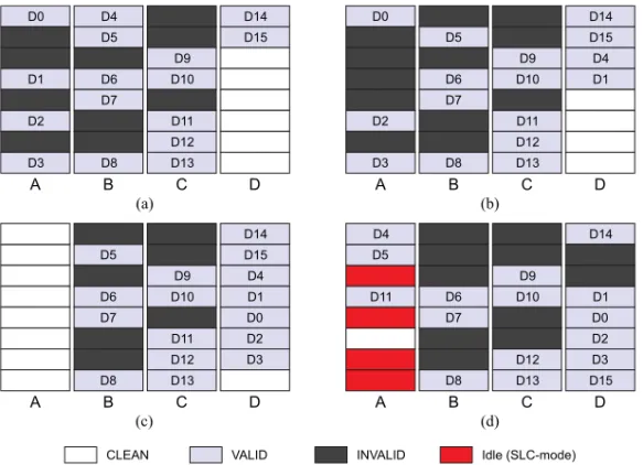
Flash Translation Layers(FTLs) map logical addresses to physical flash locations. To do this, the FTL maintains the state of every page—typical states areclean,valid, orinvalid, as illustrated in Figure 3(a). Valid pages cannot be reprogrammed without being erased, which means the FTL must always have clean pages available and will direct incoming writes to them. Whenever data is written, the selected clean page becomes valid and the old copy becomes invalid. This is illustrated in Figure 3(b), where D1 and D4 have been reallocated.
When a block is used in SLC mode, all of its MSB pages must be bypassed and are considered idle. This is illustrated in Figure 3(d), where block A has been set to SLC mode. Importantly, it is not necessary to allocate memory in the translation table to
Libra: Software-Controlled Cell Bit-Density to Balance Wear in NAND Flash 28:5
Fig. 3. Pages state transitions. (a) shows the various page states found in typical flash storage:cleanwhen it has been freshly erased,validwhen it holds valid data, andinvalidwhen its data has been updated elsewhere. In (b), data D1 and D4 are updated and their previous values are invalidated from blocks A and B. In (c), block A is reclaimed by the garbage collector. The remaining valid data were first copied to block D, before block A was erased. (d) illustrates block A set as SLC mode: half of its pages become implicitly idle.
save explicitly all MSB pages’ states; indeed, when a block is used in SLC mode, every MSB page is implicitly considered idle.
The number of invalid pages grows as the device is written. At some point, the FTL must trigger the recycling of invalid pages into clean pages. This recycling process is known as garbage collection, which selects a victim block according to a certain policy, copies any remaining valid page to available clean pages, and then erases the victim block. In the case of hybrid FTLs, this is generally triggered when the buffer becomes full. An example of garbage collection is illustrated in Figure 3(c), where block A is selected as the victim.
After a specified amount of P/E cycles, flash blocks become unreliable and their data integrity becomes compromised. FTLs implement several techniques that maximize the use of this limited endurance to guarantee a sufficient device lifetime. The typical wear-leveling algorithms implemented in FTLs target the even distribution of P/E counts over the various blocks [Wu and Zwaenepoel 1994; Chang et al. 2007]. However, despite a uniform wear, a few flash blocks normally die before the specified device endurance. Indeed, blocks do not present the same level of tolerance toward P/E cycles due to process variation, and some blocks might become unreliable significantly sooner than others. Accordingly, FTL reserves some spare blocks to replace early-failing blocks during the device lifetime [Micron 2010].
All of the blocks degrade while accumulating P/E cycles [Micheloni et al. 2010]. A block becomes progressively less efficient in the retention of charges, more sensitive to neighboring disturbances, and therefore more prone to errors. As a result, all blocks experience a gradual /Bit Error Rate/ (BER) increase with the number of P/E cycles during their life cycle. Error-Correcting Codes(ECCs) are typically used to correct a limited number of those errors within a page.
3. SLC-MLC HYBRID STORAGE
There are two main commercially successful NAND flash memory types: SLC and MLC. The devices of the latter type store multiple bits per memory cell, providing a larger bit density and hence a smaller cost per bit. Several bits can be stored in a single cell by using multiple voltage thresholds. Conventionally, the MLC refers to three voltage thresholds and stores 2 bits per cell, theTriple-Level Cell(TLC) orX3stores 3 bits per cell, andX4stores 4 bits per cell.
Manipulating MLCs is trickier than SLCs: a higher precision is required to differ-entiate the multiple voltage levels, which translates into about three to four times slower page programs and consumes more energy [Grupp et al. 2009]. Furthermore, because of reduced margins between the voltage thresholds, the MLC is more sensitive than the SLC to charge losses and neighboring cell interferences that typically affect flash reliability, which translates into about an order of magnitude shorter endurance [Grupp et al. 2012]. Therefore, the MLC offers a higher bit density than the SLC at the expense of lower performance, higher energy consumption, and reduced lifetime.
Hybrid flash devices combine one or more SLC devices to act as a buffer with one or more MLC devices to implement the data partition; their purpose is to improve the device performance: the more hot data (frequently updated data) directed to the log buffer, the closer the hybrid device performance is to that of an SLC-only device. Log buffers need to be carefully dimensioned, and the smaller the buffer partition can be made, the higher the bit density of the flash device. This is a well-understood tradeoff between cost and performance [Park et al. 2011]. Yet, the impact of such partitioning on the device lifetime is critical and must be carefully considered.
Depending on the application write pattern, an unbalanced wear can occur between the buffer and data partitions, as illustrated in Figure 1. Each partition lifetime is proportional to its technology endurance and capacity, and inversely proportional to the ratio of writes directed to it. For example, let us consider a budget of 100 cells; we allocate 5% for an SLC buffer and the rest to the MLC data partition. Considering that the endurance of an SLC is about 10 times larger than that of an MLC [Grupp et al. 2012] and, for this particular example, that each partition receives 50% of the writes, in this scenario and compared to an MLC-only device receiving 100% of the writes, the normalized MLC-data partition lifetime is
LD= CapacityDATA CapacityTOTAL WritesDATA WritesTOTAL =0.95 0.5 =1.9. (1)
On the other hand, the SLC partition allocates only 5% of the cells, and each cell has 10 times the endurance of an MLC but can store only half of the bits of an MLC, which translates to 2.5% of the capacity of an MLC-only device; accordingly, the normalized lifetime of the SLC partition corresponds to
LB= CapacityBUFFER CapacityTOTAL · EnduranceSLC EnduranceMLC WritesBUFFER WritesTOTAL = 0.025·10 0.5 =0.5. (2)
This indicates that a device with such a hybrid configuration will last half of the time of an MLC-only device, which is already significantly shorter than the lifetime of an SLC-only device.
In order to model analytically the lifetime of a hybrid flash device, we defineφSLCand
φMLCas the proportion of write directed to the buffer and data partitions, respectively,
withφSLC+φMLC=1. LetρSLCandρMLC, respectively, be the ratios of the device’s cells
allocated to the buffer and data. We defineLBand LDas the buffer and data partition
Libra: Software-Controlled Cell Bit-Density to Balance Wear in NAND Flash 28:7
Fig. 4. Hard partitions lifetime model for different buffer sizes as a function of the write ratio to the buffer. The model is normalized to a 2-bit MLC-only flash device lifetime. We illustrate the 5% buffer size lifetime construct by plotting both the buffer and data partition lifetime components. For large sequential writes, where an FTL will more likely bypass the buffer, the device lifetime is bounded to the data partition on the left. Small and frequently updated writes will wear out the buffer first, limiting the device lifetime to the buffer partition. For reasonably sized SLC buffers, lifetime is reduced by up to one order of magnitude compared to an MLC-only device.
it. The partition lifetimes are normalized to an MLC-only device’s lifetime that would receive 100% of the writes. We will use this MLC-only baseline as a lifetime reference throughout this article. Considering ann-bit per cell technology and an SLC endurance comparativelyγ times larger, the lifetime of the bufferLBis
LB=γ·ρSLC
n·φSLC
. (3)
The data partition lifetime is expressed as follows:
LD= ρMLC
φMLC.
(4) A device on hard partitions will die whenever the first of its partition wears out. Accordingly, a hard partition lifetime corresponds to the minimum out of its partition lifetime:
LH=min(LB,LD). (5)
Assuming MLC (n=2 andγ =10), Figure 4 plots Equation (5) and represents the device lifetime, normalized to an MLC-only device, for different buffer sizesρSLCand
function ofφSLC, the ratio of writes directed to the log buffer. We observe that for
rea-sonable buffer sizes (i.e.,ρSLC<10%), the lifetime of hybrid devices drops significantly
when more than 25% of writes are directed to the buffer. Around one-fifth of the cells should be allocated to the buffer to ensure a lifetime close to the MLC-only’s lifetime. Because the buffer does not account for capacity, this would result in a significant density cost.
The main issue of hard partitioning is the inability to share the wear between its partitions. This, as shown in Figure 4, can seriously compromise the viability of hybrid devices. In the following section, we introduceLibra, which builds on soft partitions to share and balance the stress on the whole device and maximize its lifetime.
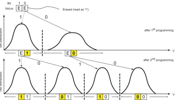
Fig. 5. Programming of a 2-bit MLC. Each bit of a cell is programmed separately. Programming the first bit, or LSB, requires one to target a single level (staying at the erased level is free) and does not need to be very precise. Programming the MSB requires one to read the current state of the cell and targets potentially three different levels, which requires more precision and time. Using cells in SLC mode consists of programming only the first bit of each cell.
4. LIBRA: SOFT PARTITIONS TO BALANCE WEAR
Librarelies on soft partitions to break the rigidity of hard partitioning by changing the physical placement of the SLC-mode log buffer depending on the device wear [Jimenez et al. 2012]. This is made possible by the fact that an MLC can be managed in software as an SLC achieving better performance. We have actually used real chips and validated experimentally that the performance of an MLC managed as an SLC is very similar to that exhibited by an SLC device. We propose the FTL to keep track of the cumulative wear (SLC and MLC mode) to decide dynamically the best physical allocation.
4.1. Faster MLC: Managing MLC as SLC
MLC can be used to store a single bit instead of two and recover the performance and energy consumption benefits of the SLC [Frankie 2007; Grupp et al. 2009]. Figure 5 illustrates the programming sequence of a 2-bit MLC. Each cell represents 2 bits, namely, the LSB and the MSB, which are allocated to different pages and are programmed separately. Before starting the actual programming, the cell needs first to be erased. Then, the LSB is programmed targeting a single voltage level, which is performed quickly, because this step does not need to be very precise. In a final step, the MSB is programmed, which requires one to first read the current state (i.e., the LSB value) and to then push the cell voltage to either of the three different levels (see solid arrows in the figure). This second programming requires higher precision and it is typically about four to five times longer than the LSB programming [Grupp et al. 2009].
Interestingly, programming only the LSB of an MLC shows performances very simi-lar to an SLC, which motivated previous researchers [Im and Shin 2010] to propose the use of an MLC as an SLC for a statically allocated log buffer partition, as illustrated in Figure 1(a). Thereby, performance is obtained at the expense of density in an MLC device. Such a way of manipulating an MLC is referred to asSLC modein this article. In this work, we propose to go one step further and dynamically change the physical allocation of the buffer to globally balance the wear. Accordingly, when a block allocated
Libra: Software-Controlled Cell Bit-Density to Balance Wear in NAND Flash 28:9
Fig. 6. Hard and soft partitioning architecture examples. Hard partitioning relies on a mix of SLC and MLC devices, while soft partitioning is built on a homogeneous MLC fabric. In both examples, the storage controller is connected to three channels with four flash chips each. On hard partitions, only one chip is an SLC, which is the only one allocated to the buffer. On the soft partitioning, the buffer can be distributed on every chip. This enables multiple advantageous features that are not covered in this article, such as cheap on-chip buffer-to-data migrations, large write bandwidth to the buffer, or a resizable buffer.
to the buffer has accumulated significantly more wear than a data block, both blocks will be swapped.
4.2. Software-Controlled Log Buffer
Whereas hard partitioning is typically built on heterogeneous SLC and MLC hardware, the soft-partition scheme applies to a completely homogeneous hardware architecture made only of one or more MLC chips. Figure 6 illustrates soft and hard partitioning ex-amples for a possible architecture made of a microcontroller connected to three channels of several flash chips. In Figure 6(a), the device built on hard partitions has multiple MLC chips and a single SLC chip, whereas in Figure 6(b), the device is composed exclu-sively of MLC chips and uses soft partitions. Architecturally, a soft partitioning offers many benefits. For example, as opposed to hard partitions, the bandwidth to the buffer is not limited to one channel. Instead, multiple channels can be accessed in parallel to write the buffer, as well as multiple chips in an interleaved fashion. Furthermore, the evictions from the buffer do not necessarily require an expensive off-chip migration but can potentially be performed on-chip. Finally, a soft partitioning does not restrict the buffer size to a physical constraint; hence, in order to improve performance, the buffer size could be expanded when the device capacity is not completely used or by using MLC mode for some of the buffer blocks, dynamically trading off write latency for buffer capacity. Yet, in this work, we decided to not cover those advantages and focus on the raw benefits of the soft partitioning, that is, to be able to write selectively regions of the flash chip(s) to SLC mode or MLC mode at will, with the intention to evenly distribute the wear throughout the whole device. While small buffers are likely to die first for hard partitions, a soft partitioning can spread the localized stress over the complete device.
Classical wear-leveling algorithms periodically switch cold and hot blocks in order to even their P/E cycle counts and balance the wear on the whole device. Typically, when a hot block is evicted from the log buffer and erased, the wear-leveling logic compares P/E counts of this block with the coldest block (i.e., with the smallest P/E count) and decides whether to swap them, for example, when the P/E count difference reaches some threshold. Upon a swap, every page of the cold block is copied into the evicted hot block, and the cold block is then erased and allocated to the buffer. Figure 7 illustrates the evolution of a device mixing SLC and MLC mode on soft partitions and shows how a careful wear balancing can avoid the premature death that is likely to happen
Fig. 7. Software-controlled log buffer. A practical scenario of a hybrid FTL, where blocks regularly alternate between SLC and MLC mode in order to balance the overall wear.
in the hard-partitioned architectures proposed in all previous work. Focusing on the leftmost physical block, one can see how this is initially allocated to the buffer, and thus managed as an SLC, and then is invalidated and freed from both partitions to be later allocated to the data partition, managed as an MLC. Such transitions are naturally triggered by the wear-leveling algorithm. Notice that the wear of the block increases through time and is a result of both the periods when the block is programmed as an SLC and as an MLC.
4.3. Libra Implementation
ImplementingLibra in hybrid FTLs is very simple, because hybrid FTLs already in-corporate the data structures and mechanisms required for it. Regarding the mode identification (i.e., SLC or MLC), hybrid FTLs use 1 bit in the spare bytes of the first page of a block to differentiate a log buffer block from a data block. Because every log buffer block is used in SLC mode withLibra, the SLC-MLC classification is implicit to this differentiation. The only difference with a hybrid FTL using exclusively MLC mode is that only half of the raw log buffer capacity will be used. Accordingly, whenever we access a log buffer block, only LSB pages will be referenced.
Although implementingLibraon hybrid FTLs is straightforward, it does not mean thatLibrais bounded to this class of FTLs. In fact, it can perfectly be implemented by any type of FTL, such as page-level mapped FTLs. The only requirement is to be able to differentiate blocks allocated in SLC and MLC mode and have a level of decision in choosing whether data should be written in either of these modes. Generally, page-level mapped FTLs implement a hot/cold filter, much like hybrid FTLs, to regroup data likely to be updated soon together in the same blocks, resulting in hot blocks made of many invalidated pages, which reduces garbage collection overhead. Accordingly, for those FTLs, data categorized as hot could be written in SLC mode. However, as opposed to classical hybrid FTLs and hard partitions, the number of hot blocks would not be bounded to a fixed number. Such flexibility can be exploited by the garbage collection process to reduce overheads. However, this work will only evaluate the use ofLibrain hybrid FTL architectures, as their performance is not improved by the flexibility of the SLC mode. Thereby, we can concentrate on the lifetime improvements of our approach.
Libra: Software-Controlled Cell Bit-Density to Balance Wear in NAND Flash 28:11
Finally, the FTL needs to consider a global wear metric that includes the effects of both the MLC mode and SLC mode to be able to implement a regular wear-leveling algorithm. Such metric is the foundation of our proposedLibraand will be detailed in the following subsection.
4.4. Libra Lifetime Model
We evaluate the lifetime of a flash device by the total amount of data written before wearing out. This lifetime is inversely proportional to the average wear experienced when writing a bit in a cell. Intuitively, this wear is correlated to the amount of charges being stored in a cell. Hence, a partial programming (i.e., SLC mode) should generate less wear than a full programming (i.e., MLC). This is verified experimentally on real chips in Section 5. LetωSLCbe the relative wear generated when writing a bit in SLC
mode with respect to the wear per written bit in MLC.Libra uses blocks alternately in SLC or MLC mode, while still being able to evaluate the cumulative wear of each individual block. Hence, the lifetime of a device implementing Libra is a function of the write ratio directed to the buffer, φSLC. In the one extreme, when the MLC
mode is exclusively used (φSLC =0), the device lifetime is trivially equal to an
MLC-only device. In the other extreme, when the SLC mode is exclusively used (φSLC =
1), the device lifetime is defined by the wear of the SLC writes and corresponds to
1
ωSLC. Note that despite the larger read margin of the SLC mode (larger than MLC, as discussed in Section 4.1), this lifetime is different than a regular SLC device, because every block can potentially later be allocated to an MLC and is thereby restrained to the MLC endurance. The device lifetime is inversely proportional to the average wear experienced. Given the write ratio directed to the buffer,φSLC, the average wear
normalized to the MLC wear is
1−φSLC+ωSLC·φSLC=1−φSLC·(1−ωSLC). (6)
Trivially, the lifetime of Libra, L, normalized to MLC only is the inverse of Equation (6), which is
L(φSLC)=
1
1−φSLC·(1−ωSLC)
. (7)
When ωSLC ≤ 1, Libra ensures a lifetime larger than or equal to MLC only.
How-ever,ωSLC is a parameter that cannot be found in typical specifications of MLC flash
chips, as manufacturers generally do not publish the SLC-mode characteristics in their documentation. In the next section, we will describe how to extract this parameter ex-perimentally from actual flash chips.
5. SLC-MODE CHARACTERIZATION
In order to evaluate the relative wear of SLC modeωSLC with respect to an MLC, we
built an FPGA-based platform to interface ONFI [ONFI workgroup 2013]-compliant NAND flash chips and we extracted experimentally this parameter for two 30nm class NAND flash chips from different manufacturers, whose characteristics are listed in Table I.
The experiment consists of programming continuously a set of 50 flash blocks either in SLC or MLC mode while periodically measuring the BER. Specifically, we write random data in every block, read them back to identify and count fault bits, erase the blocks, and start over. We characterize several rates of SLC mode by setting for each block a fixed predefined SLC-mode frequency ranging from 0% to 99%. We report the results in Figure 8 for five different SLC-mode frequencies and for the two chips. The graphs show how the BER evolves with respect to the P/E cycles for the different sets of blocks. The BERs are averaged over periods of 100 P/E cycles and, in order to
Table I. MLC NAND Flash Chip Characteristics
Features C1 C2
Total size 32GB 32GB
Pages per block 128 256
Page size 8kB 8kB Spare bytes 448 448 Read latency 130μs 40–60μs LSB write lat. 330μs 360μs MSB write lat. 1,750μs 1,800μs Erase latency 4ms 3ms Architecture ABL HBL
Fig. 8. Comparison of SLC- and MLC-mode cell degradation speed. P/E cycles are applied on five sets of blocks, each with a different SLC-mode cycle frequency. The BER is evaluated exclusively during MLC cycles. C2 degrades significantly faster than C1. For each chip, we report the fitted constant parameters and the variable parameter A, which varies with the SLC-mode ratio. As anticipated, SLC-mode cycles generate clearly less stress to the cells than MLC cycles.
measure the relative wear of the cells with the same reference for every block, only MLC cycles are considered. Indeed, the SLC-mode superior reliability systematically generates fewer bit errors than the MLC. From the figure, we distinctly see an effect from the SLC-mode frequency on the degradation speed: the more frequently the SLC mode is used, the slower the degradation becomes.
In order to quantify the effects of the SLC mode on the device wear, we fit our results on flash degradation models. In previous work related to flash memory characterization [Mohan et al. 2010], the growing BER in function of P/E cycles is generally modeled by the power function
BER(x)=αxβ+C. (8)
While this function fits the BER of individual pages relatively well, in our case, it did not when averaging the BER of a set of pages. For the studied flash chips, we found that adding a term of degree 1 to the power function fits accurately the average BER and becomes
BER(x)=αxβ+γx+C. (9)
We observed that the effects of SLC mode will stretch linearly the reference curve on the P/E cycle axis. Accordingly, we adapt Equation (9) to propose the equivalent form
Libra: Software-Controlled Cell Bit-Density to Balance Wear in NAND Flash 28:13
Fig. 9. Considering recovery effects. We evaluate the combined effects of recovery and SLC-mode cycling on cells. We accelerate the recovery by baking periodically the chips. The baking events are marked by the vertical bars. The recovery effect is significant for C2, whereas for C1 it becomes observable only after 15,000 cycles. The reference curve corresponds to normal cycling without baking episodes. For visibility, the full data from baked C2 blocks is only reported for the 0% SLC-mode set. Only the data points measured right after the baking are considered to evaluate the blocks’ degradation speed. The relative wear of SLC mode remains stable with the recovery process, and it even gets slightly lower for C2, which means that SLC mode is even less harmful when considering recovery time.
whereβ,γ, andCare constant for a chip. The Acoefficient represents the degradation speed and varies in function of the SLC-mode frequency. This is the effect that we want to evaluate here. Fitting every set of data to Equation (10) and fixing the constant factors to the most satisfying values results in a marginal sum of squared residuals. The fitted curves and their corresponding parameters are provided in Figure 8. Our experiment confirms that SLC-mode cycles generate less stress than regular MLC cycles and allows us to quantify it.Librawill use this information to evaluate blocks’ wear based on their SLC and MLC cycle counts. However, this experiment aggressively wears out the blocks by continuously writing them, which is not representative of a realistic usage of the device. Therefore, we propose in the next subsection another experiment that validates our measurements for a realistic usage.
5.1. Considering the Recovery Factor
Although applying P/E cycles continuously on flash cells allows us to reduce the ex-periment time, it does not represent a realistic scenario. In a real system, the cells are written at a much lower frequency, which gives time for trapped charges to leave the oxide after a while, healing the cells. This phenomenon is known as therecovery process[Mielke et al. 2006; Mohan et al. 2010].
In order to take into account the recovery effect when evaluating the SLC-mode wear, we conducted a second experiment, similar to the first one except that it includes periodic baking times. Every few thousands of P/E cycles, we paused the experiment, removed the daughter board with the flash chips from the FPGA board, and baked them at 125◦C for 5 hours. Baking the chips allows us to significantly accelerate the recovery process [Mielke et al. 2006]. From now on, we will refer to the previous experiment as thefastexperiment and the presently described experiment as thebakedone.
We report our measurements in Figure 9. The recovery effect is significant for chip C2, whereas for C1, the effect is noticeable only after 15,000 P/E cycles. The reference curve is taken from thefastexperiment, without SLC-mode cycles or baking periods. For C2, the BER drops correspond to the baking events (marked by vertical bars), while the rapid BER growth corresponds to the aggressive P/E cycling. For visibility convenience,
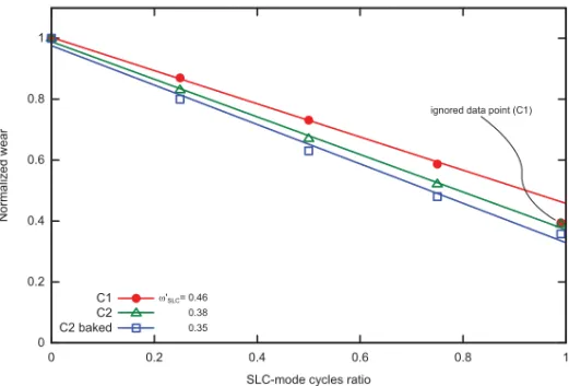
Fig. 10. Evaluation of SLC-mode wear. We plot the average wear in function of the SLC-mode P/E cycles ratio as measured on our two chips and provide the corresponding SLC-mode P/E cycle wear coefficient (ωSLC) for each dataset. For the C1 chip, thefastandbakedexperiments gave identical results. Thereby, thebaked experiment data is only shown for C2. We observe for C1 an irregularity when measuring the endurance at 99% SLC-mode cycle ratio. Specifically, for this chip, the SLC-mode wear is reduced when approaching extreme SLC-mode ratios, while the wear factor stays constant on lower ratios. This effect is not observed on C2, where the SLC-mode wear coefficient stays constant. Hence, in order to stick with our simple model, we ignore this irregular (yet favorable) data point and evaluate for C1 a pessimistic SLC-mode wear that is accurate for the majority of SLC-mode ratios.
the full C2 baked data is only provided for the set without SLC-mode cycles (0%). We only consider the BER when cells are freshly baked to fit the data on the model of Equation (10). Similarly to thefastexperiment, we can observe that SLC-mode cycles infer less stress than regular MLC-mode cycles. Based on those measurements, we will precisely quantify and discuss the resulting SLC-mode wear in the next subsection. 5.2. SLC-Mode Wear
From our two experiments, we observed that the ratio of SLC-mode cycles has an effect on the degradation speed, which we quantified with the fitted parameterA. This parameter is directly proportional to the average wear of a P/E cycle. Hence, the smaller
Ais, the less the damage on a cell there is and the larger the endurance. For example, looking at the fitted parameters of C2, a 75% SLC-mode ratio (A75=1.15·10−6) almost
halves the wear compared to a 0% SLC-mode ratio (A0=2.21·10−6). Accordingly, blocks
with a 75% SLC-mode ratio will require about two times the P/E cycles to reach the same BER than a block with a 0% SLC-mode ratio. In order to evaluate ωSLC, the relative wear of an SLC-mode P/E cycle compared to the MLC, we express the average wear in function ofφSLC , the ratio of SLC-mode cycle, as
AvgWear(φSLC)=1−φSLC +φSLC ·ωSLC, (11) with 1−φSLC corresponding to the MLC wear contribution and φSLC·ωSLC to the SLC-mode contribution. For each chip, we fit Equation (11) on the extracted A pa-rameters with a linear regression to extractωSLC. Accordingly, we plot the fitted A
parameters and their corresponding fitted curve in Figure 10 and also report the cor-respondingωSLC. The data is normalized to the corresponding 0% SLC-mode ratio. The standard deviation associated to every data point is very small (less than 2%). The
Libra: Software-Controlled Cell Bit-Density to Balance Wear in NAND Flash 28:15
Fig. 11. Libraversus hard partition lifetime. We provide the expectedLibralifetime corresponding to our chips’ characterization and compare them to hard partitioning. The lifetime is normalized to an MLC-only device. As opposed to hard partitions, theLibralifetime is not a function of the buffer size but solely of the ratio of writes to the SLC buffer. We provide for eachLibralifetime curve the corresponding SLC-mode wear coefficientωSLC. The lifetime evaluation corresponding to thebakedexperiment of C2 is dashed and indicates that the recovery effect observed in typical flash usage increases the lifetime extension provided byLibra. Accordingly, the lifetime evaluated from afastexperiment can be considered as a conservative estimation.
difference between thebakedandfastresults for C1 is not observable; hence, the C1
bakedresults have been omitted.
We observe a slightly smaller SLC-mode wear when we let C2 recover, while for C1 the difference is negligible. In the case of C1, we also notice that the SLC-mode wear is not constant: the data point out that 99% of the SLC-mode cycle ratio is not aligned with the previous ones. Specifically, the SLC-mode wear coefficient decreases when approaching extreme SLC-mode ratios. Conservatively, although this fact would benefit the lifetime ofLibra, we prefer to ignore this particular data point when evaluatingωSLCin order to provide a more accurate SLC-mode wear information on the lowest SLC-mode ratios.
AfterωSLCis measured, an FTL is then able to convert a mixed SLC- and MLC-mode wear into a global wear expressed in MLC P/E cycles. While typical FTLs keep a single P/E counter for each block in order to balance the wear,Libra needs two counters in order to differentiate SLC- and MLC-mode P/E counts, which represents a negligible overhead of about 16 bits per block. Accordingly,Libraexpresses the global wear of a blockBwith
Wear(B)=CountMLC(B)+ωSLC·CountSLC(B). (12)
Thereby, when typical FTLs perform their wear leveling based on the MLC P/E count of every block,Librauses the result of Equation (12) instead.
Regarding the lifetime that can be expected byLibrafor each chip, we rely on the lifetime model of Equation (7). First, we need to convertωSLC(SLC-mode wear per P/E cycle, normalized to MLC) intoωSLC (SLC-mode wear per written bit, normalized to
MLC). Trivially, knowing that MLC writes 2 bits per cycle, we use
ωSLC=2·ωSLC. (13)
Correspondingly, we report theωSLCcoefficients in Figure 11 and compare their
Table II. Benchmark Characteristics
Data Written Footprint Footprint Average Request Request Size
Benchmark [MB] [MB] Ratio Size [kB] Variance [kB]
homesrv 5,566 1,115 0.20 18.6 −13.7/+105.2 copy 3,606 3,598 1.00 395.6 −339.7/+115.3 fin1 14,918 527 0.04 3.7 −1.6/+6.1 fin2 1,860 369 0.20 2.9 −2.0/+10.1 hm_0 20,968 1,670 0.08 8.3 −5.1/+28.4 mds_0 7,542 339 0.04 7.2 −3.8/+10.1 prn_0 47,068 12,683 0.27 9.7 −7.4/+35.2 proj_0 147,729 1,693 0.01 40.9 −31.7/+22.4 prxy_0 55,088 723 0.01 4.6 −3.3/+24.8 prxy_1 742,211 13,078 0.02 13.1 −6.8/+41.3 rsrch_0 11,077 296 0.03 8.7 −4.2/+19.5 src1_2 45,206 669 0.01 32.5 −24.7/+29.4 src2_0 9,563 504 0.05 7.1 −3.6/+9.3 stg_0 15,452 401 0.03 9.2 −5.2/+24.5 stg_1 6,129 405 0.07 7.9 −3.9/+14.9 ts_0 11,611 549 0.05 8.0 −3.6/+21.1 usr_0 13,390 661 0.05 10.3 −5.8/+18.8 wdev_0 7,317 351 0.05 8.2 −4.2/+15.2 web_0 11,952 711 0.06 8.6 −4.2/+20.6
lifetime and as described by Equation (7), theLibralifetime does not directly depend on the buffer size. Instead, for the same application, a different buffer size would translate into a new SLC-mode cycles ratio, which directly impacts our lifetime extension. Both C1 and C2 curves behave almost linearly, and C2 provides more than 10% extra lifetime for 50% of SLC-mode cycles compared to MLC only. C1 shows a smaller efficiency and is slower to provide extra lifetime. Nonetheless, both have theirωSLCcoefficients smaller
than one and thus show a lifetime that is systematically larger than the MLC-only ref-erence. Importantly, evaluating the lifetime from afastexperiment can be considered a worst-case scenario, where blocks are written at unrealistic frequencies, and provides a conservative lifetime. Accordingly, when we consider significant write ratios to the buffer and for reasonably sized buffers,Libraprovides up to one order of magnitude more lifetime than hard partitions. In the next section, we stress a simulated flash device from a set of realistic traces in order to evaluate more precisely the lifetime extension provided byLibra.
6. RESULTS
In this section, the proposed soft partitioning techniqueLibrais combined with three published FTLs and the results of running 19 different data traces from three different suites are compared to the hard partitioning architecture.
6.1. Experimental Setup
We developed a trace-driven flash simulator in order to measure the execution time and erase counts of several FTLs executing realistic traces, whose characteristics are listed in Table II. We generated the “homesrv” and “copy” traces from a tiny server running on a Linux distribution having its root on a flash storage of 16GB and hosting various standard services (e.g., file server, mail, web). The “homesrv” trace contains 1 week of this server’s system storage activity. The second trace, “copy,” was obtained from writing several gigabytes of MP3 files. The next two traces, “fin1” and “fin2,” were obtained from the UMass Trace Repository [Bates and McNutt 2007] and produced from OLTP applications running at a large financial institution. The last 15 traces were taken
Libra: Software-Controlled Cell Bit-Density to Balance Wear in NAND Flash 28:17
from the MSR Cambridge traces set [Narayanan et al. 2008], which contains 1 week of their data center activity.
Some of the characteristics of the selected benchmarks are included in Table II. The ratio between memory footprint and total data written gives an indication of the write updates’ locality. A value close to zero corresponds to a high locality, and a value close to one corresponds to no locality. The average and the standard deviation of the request size indicate how different are the sizes of the different requests. Looking at the traces’ characteristics, we can conclude that “copy” includes large sequential memory requests and no update locality, “fin2” and “prn_0” have a mild update locality, and the rest of the traces have a high locality with memory requests of various sizes. Except for our own traces, most of the traces were gathered from magnetic disks and their file systems were generally not optimized for flash. For example, traces based on disks using a sector size of 4kB would have a misaligned address space (i.e., sector addresses are not divisible by 4kB). Accordingly, we realigned the disks’ address space in order to avoid having 4kB write accesses systematically overlapping over two flash pages.
We implemented three different hybrid FTLs, namely, FAST [Lee et al. 2007], ROSE [Chiao and Chang 2011], and ComboFTL [Im and Shin 2010]. FAST is a reference hybrid FTL, which maps its data partition to the block level. It is light, is simple to implement, and suits low-cost storage solutions. ROSE is one of the latest improve-ments of FAST known to these authors. It decreases the garbage collection overhead by using a more advanced and efficient metric to select victim blocks from the buffer. Although both those FTLs originally used a regular MLC buffer, we allocate the buffer to an SLC, which, as motivated by Section 4.1, increases performance and reduces power consumption. The only side effect is that twice as many blocks must be allocated to the buffer, effectively reducing the device capacity, which we assume to pay off for reasonable buffer sizes. Lastly, ComboFTL includes an SLC buffer that gives multiple chances to victim data upon eviction. If the victim data is considered as being likely to be updated, it can be fed back into the buffer, avoiding an expensive migration to the MLC partition. ComboFTL has a parameter to control the write bandwidth directed to the buffer and data partitions. Considering hard partitions, while directing writes to the buffer more often might increase performance, it is also likely to reduce the device lifetime, and reversely. Thus, as opposed to the other two FTLs, ComboFTL can trade off performance for lifetime. Finally, the ComboFTL address mapping is built on a hierarchy of mappings that provides a thinner granularity than the block level: the data partition is divided into sets of several blocks and each set has its own page-level mapping table. This mapping reduces the garbage collection overhead compared to FAST and ROSE but requires more RAM to store the translation table.
The simulated flash characteristics match the C2 chip and the simulated device has a capacity of 16GB. Except for our own traces, most of the considered traces come from disks much larger than 16GB (up to 1TB). Still, every trace’s footprint is smaller than 16GB. Hence, when we partition the original disks’ storage in blocks of the same size as the considered flash (i.e., 2MB blocks in our case) and consider only the referenced blocks, every trace fits in the simulated device. We perform this compression on the block level rather than the sector level in order to not alter data locality, which would have changed the traces’ behavior. Thereby, the only difference coming from our relatively small simulated device is that the absolute buffer capacity for a 16GB disk would be smaller than the original disks’ buffer. A smaller buffer will incur a higher garbage collection overhead: for the same trace, the victim blocks selected by the garbage collector will more likely contain valid pages to merge into the data partition. Consequently, the data partition will be written more often and the write ratio to the buffer will decrease, which penalizes the soft-partition relative lifetime. Note that in Figure 11, the lifetime extension ofLibramonotonically increases with the ratio of
writes directed to the buffer. Furthermore, as seen in the hard-partition lifetime model, a write ratio to the buffer that is too high reduces its lifetime dramatically compared to MLC only. Accordingly, the chosen simulated disk capacity will be advantageous to the hard partitions, underestimating the lifetime extensions that can be achieved with our proposed approach.
6.2. Soft- Versus Hard-Partitioned Hybrid FTLs
The traces are executed by each FTL for several buffer sizes ranging from 1% to 20% of the device’s cells. The traces are executed twice: the first run serves as a warmup and we collect the result with the second run. We assume that the data partition is originally fully allocated with valid data. This assumption is conservative compared to a typical use case and provides a conservative lifetime forLibra. Indeed, a fully allocated device increases the garbage collection overhead and provides a smaller write ratio to the buffer. We visit a large spectrum of parameters specific to each FTL and keep only the most effective combination for each trace. For FAST and ROSE, reducing execution time will systematically maximize lifetime, whereas for ComboFTL, originally built on hard partitions, it provides parameters to limit excessive writes to the SLC partition to try to balance the wear between the two partitions, trading off performance in the process. Accordingly, we present in our results two parameter sets for ComboFTL: ComboLmaximizes lifetime, while ComboP maximizes performance.
We implemented a classical wear-leveling strategy, where we limit the P/E count’s difference between the blocks to 100 cycles [Wu and Zwaenepoel 1994]. Whenever the P/E count difference between a block freshly erased and the block currently having the lowest P/E count exceeds this limit, the former block replaces the latter, which is in turn erased and ready to be allocated. On hard partitions, such a wear-leveling approach must be separately performed on each partition; instead, for Libra, it is performed globally, similarly to a regular MLC-only device. This difference has a very small impact on the lifetime and performance difference betweenLibraand the hard partitioning. We measured a difference that is systematically below 1% of the execution time and lifetime. Thus, the execution time of both theLibraand the hard partitioning scheme is assumed to be the same in our experiments.
Figure 12 shows a normalized lifetime (top) and normalized execution time (bottom) of the selected FTLs executing the traces of Table II for a buffer size of 5% of the device’s cells. For every combination of FTL and trace, we report the lifetime corresponding to
Libra() and hard partitions (H). The lifetime results are normalized to ComboP on
hard partitions and the execution time is normalized to ComboP. In this figure, we
report the results ofLibrafor C2 only.
We observe that the proposed soft partitioning is able to considerably increase the device lifetime with respect to hard partitioning for the vast majority of the traces and FTLs. When a lot of stress is put on the buffer, ComboL is able to extend hard
partitions’ lifetime compared to ComboP, sacrificing significantly the performance. On
average, on hard partitions, ComboLalmost doubles the lifetime compared to ComboP
while increasing the execution time by 25%, whereas ComboP on Libra quadruples
the lifetime on average compared to hard partitions and with similar performance. Interestingly, maximizing the lifetime for hard partitions does not improve the lifetime forLibra. Indeed, ComboLlimits the write bandwidth to the buffer, whileLibrabenefits
from the fact that SLC-erase cycles wear less the cells while improving performance. When hard partitioning requires trading- off lifetime for performance,Librais able to obtain the best of both; therefore, the results for ComboLonLibraare omitted from the
lifetime results.
The “copy” trace being mostly made of very large sequential accesses, it bypasses completely the buffer and directs most of the accesses to the data partition. Having the
Libra: Software-Controlled Cell Bit-Density to Balance Wear in NAND Flash 28:19
Fig. 12. Lifetime and performance. The results contrast our technique (“” versions) versus hard partition-ing (“H” versions) for three FTLs implemented with a 5% buffer size and normalized to ComboP on hard
partitions. Among a large spectrum of parameters specific to each FTL, only the best results are shown. ComboP and ComboLmaximize performance and lifetime, respectively. In the case of performance, we
as-sume the difference between hard and soft partitioning to be negligible. The soft partition results correspond to theωSLCmeasured from C2. Overall, our soft partitioning significantly increases lifetime for practically every considered FTL and benchmark.
majority of writes directed to the MLC partition annihilates most of the benefit of an SLC-MLC combined architecture, and it is not surprising to observe a similar lifetime between hard and soft partitioning.
6.3. Generalization of Experimental Results
Figure 13 plots over Figure 4 the lifetime results for the different configurations dis-cussed in the previous subsection. New configurations corresponding to additional log buffer sizes are also added to the figure.
For applications with high update locality, we observe that increasing the buffer size reduces the pressure on the data partition and results in higher ratios of writes to the buffer. This is represented by the data points shifting to the right (i.e., larger write buffer ratio) when going to larger buffer sizes. In that spectrum of the plot, hard partitioning is only able to outperform soft partitioning for very large buffer sizes. Such region is shaded in the figure and annotated ashigh cost. It should be noted that the majority of the points outperforming soft partitioning are from FAST and ROSE, which are, in absolute, less efficient (i.e., worse performance and lifetime) than ComboFTL. When hard partitioning fails to maximize the device lifetime for sensible buffer sizes,
Libracan extend it by up to 10×. Such region is shaded in the figure and annotated astypical. The latter corresponds to scenarios that are likely to target a hybrid device to increase the flash performance and that, importantly, will largely extend the device lifetime when adopting the proposed soft partitioning.
Fig. 13. Lifetime models populated by benchmark results. This graph shows the result of every best com-bination of FTLs, traces, and buffer sizes normalized to MLC only. In typical applications including random access patterns, soft partitions do systematically better. Only configurations characterized by a considerably higher cost can reach higher lifetimes.
For sequential access patterns, all the buffer sizes present a very low ratio of buffer writes, which results in marginal differences between the different cases, except for large buffer sizes. Such region, shaded in the figure and annotated assequential, does not benefit from the hybrid device schemes targeted in this article.
7. RELATED WORK
The idea of an SLC-MLC combined architecture has been investigated in previous work. Grupp et al. [2009] experimentally characterize a set of flash chips reporting performance and energy figures and notice the variable performance in MLC flash between LSB and MSB page programmings. Based on those observations, they propose Mango, an FTL that opportunistically skips MSB pages to enhance the responsiveness and reduce the total energy consumed. As opposed to the SLC mode presented in our work, Mango can bypass an MSB page of a block independently of the other MSB pages. In other words, in Mango, blocks can have valid and bypassed MSB pages at the same time. Consequently, the SLC-mode reduced wear that we characterized in our study cannot be considered by Mango to balance the blocks’ wear, which results in a lifetime reduction of about 35% with respect to MLC only.
Chang [2010] proposes a hybrid SSD combining SLC and MLC chips, which is a clear example of the hard partitioning discussed in this article. In order to extend the lifetime, they adapt the ratio of writes directed to the log buffer to balance the wear on each partition. Thereby, in most cases, performance is reduced. Instead, our proposed scheme respects the ratio of writes to the log buffer, which should have been optimized for performance by the FTL, and changes the physical allocation of the log buffer to balance the device wear, obtaining high performance without compromising device lifetime.
Murugan and Du [2012] understand the shortcomings of hard partitions in hybrid devices and developed Hybrot accordingly. It uses an integral controller that limits the flow to the SLC partition depending on the workload behavior and the hard partitions’ dimensions. Still, it uses hard partitions, and with this limited SLC-write flow, the
Libra: Software-Controlled Cell Bit-Density to Balance Wear in NAND Flash 28:21
potential benefits from an SLC cannot be fully exploited as opposed to the use of soft partitions.
Park et al. [2011] propose HFTL, an FTL based on an SSD architecture very similar to Chang’s. In particular, they propose techniques to exploit multibank parallelism and maximize bandwidth. As we do too, they realize that the device lifetime is limited by the partition with the shortest lifetime; however, they mitigate the problem by sizing the SLC partition to guarantee a lifetime larger than the MLC partition. This oversizing, with 10% to 30% of the cells allocated to the log buffer, significantly increases the cost of the system, not only for the increase in flash cells but also for the large address translation table associated, which might be prohibitive for some storage classes.
Similarly, Im and Shin [2010] propose ComboFTL, which can be tuned to optimize either lifetime at the expense of reducing performance or performance at the expense of reducing lifetime. Figure 12 shows that the combination of ComboFTL optimized for performance with our soft partitions can simultaneously achieve the longest lifetime and the best performance.
Instead of relying on an FTL to interface between a common file system and the flash memory, it is also possible to use specialized file systems that are able to directly interface the NAND flash interface and capable of supervising the wear leveling and garbage collection. The JFFS2 [Woodhouse 2001] is an example of such a flash file system and was extended by Lee et al. [2009] as FlexFS, a flash file system that enhances the storage responsiveness by selectively choosing to write data into SLC mode or MLC mode depending on the device’s capacity available. Unlike the hybrid devices previously mentioned, both cold and hot data are stored in SLC mode, which increases significantly the garbage collection overhead and consequently sacrifices the device’s lifetime. Furthermore, the wear of SLC-mode cycles is assumed equal to regular MLC-mode cycles, which prevents exploiting the flash endurance to its fullest. With a little effort, FlexFS could be adapted to implement the mechanisms ofLibrato balance the mixed wear and make better use the device’s endurance.
To the best of our knowledge, this is the first work that introduces a soft SLC/MLC partitioning of the log buffer present in hybrid FTLs; withLibra, the log buffer is con-tinuously reallocated to distribute the device wear, thus extending the device lifetime at virtually no cost.
8. CONCLUSIONS
Flash architectures combining SLC and MLC technologies are targeting new cost-sensitive applications with large data update locality. Frequent updates benefit from the superior SLC performance while devices are primarily in MLC mode to take ad-vantage of the lower cost of MLC devices. However, unbalanced pressure on the SLC partition may lead to a premature death of the device. In this article, we have pre-sentedLibra, an approach that is robust to unbalanced stress. Using data extracted from measurements on actual flash chips and making conservative estimations, Li-brashows a lifetime at least as long as that of an MLC-only device and shows up to 10 times longer lifetime compared to known SLC-MLC approaches. Furthermore, this advantage comes at practically no extra cost and without any performance loss, which is particularly interesting for high-volume consumer products.
REFERENCES
Ken Bates and Bruce McNutt. 2007. OLTP Application I/O. Retrieved from http://traces.cs.umass.edu/ index.php/Storage/Storage.
Li-Pin Chang. 2010. A hybrid approach to NAND-flash-based solid-state disks.IEEE Trans. Comput.59, 10 (Oct. 2010), 1337–1349.
Yuan-Hao Chang, Jen-Wei Hsieh, and Tei-Wei Kuo. 2007. Endurance enhancement of flash-memory storage, systems: An efficient static wear leveling design. InDesign Automation Conf.San Diego, CA, 212–217. Mong-Ling Chiao and Da-Wei Chang. 2011. ROSE: A novel flash translation layer for NAND flash memory
based on hybrid address translation.IEEE Trans. Comput.60, 6 (June 2011), 753–766.
Hyunjin Cho, Dongkun Shin, and Young Ik Eom. 2009. KAST: K-associative sector translation for NAND flash memory in real-time systems. InDesign Automation and Test in Europe. 507–512.
Roohparvar Frankie. 2007. Single level cell programming in a multiple level cell non-volatile memory device. US Patent 11/298,013. (June 14, 2007).
Laura M. Grupp, Adrian M. Caulfield, Joel Coburn, Steven Swanson, Eitan Yaakobi, Paul H. Siegel, and Jack K. Wolf. 2009. Characterizing flash memory: Anomalies, observations, and applications. InACM/IEEE Int. Symp. Microarchitecture. New York, NY, 24–33.
Laura M. Grupp, John D. Davis, and Steven Swanson. 2012. The bleak future of NAND flash memory. In USENIX Conf. on File and Storage Technologies. San Jose, CA.
Soojun Im and Dongkun Shin. 2010. ComboFTL: Improving performance and lifespan of MLC flash memory using SLC flash buffer.J. Syst. Archit.56, 12 (Dec. 2010), 641–653.
Xavier Jimenez, David Novo, and Paolo Ienne. 2012. Software controlled cell bit-density to improve NAND flash lifetime. InDesign Automation Conf.San Francisco, CA, 229–234.
Jesung Kim, Jong Min Kim, Sam H. Noh, Sang Lyul Min, and Yookun Cho. 2002. A space-efficient flash translation layer for CompactFlash systems.IEEE Trans. Consum. Electron.48, 2 (May 2002), 366–375. Sungjin Lee, Keonsoo Ha, Kangwon Zhang, Jihong Kim, and Junghwan Kim. 2009. FlexFS: A flexible flash
file system for MLC NAND flash memory. InUSENIX Annual Technical Conf.San Diego, CA.
Sungjin Lee, Dongkun Shin, Young-Jin Kim, and Jihong Kim. 2008. LAST: Locality-aware sector translation for NAND flash memory-based storage systems.ACM SIGOPS Operating Syst. Rev.42, 6 (Oct. 2008), 36–42.
Sang-Won Lee, Dong-Joo Park, Tae-Sun Chung, Dong-Ho Lee, Sangwon Park, and Ha-Joo Song. 2007. A log buffer-based flash translation layer using fully-associative sector translation.ACM Trans. Embedded Comput. Syst.6, 3 (July 2007), Article No. 18, 18:1–29.
Rino Micheloni, Luca Crippa, and Alessia Marelli. 2010.Inside NAND Flash Memories. Springer.
Micron. 2010. Bad Block Management in NAND Flash Memory. Retrieved from http://www.micron.com/ products/support/technical-notes/.
Neal Mielke, Hanmant P. Belgal, Albert Fazio, Qingru Meng, and Nick Righos. 2006. Recovery effects in the distributed cycling of flash memories. InIEEE Int. Reliability Physics Symp. Proc.San Jose, CA, 29–35. Vidyabhushan Mohan, Taniya Siddiqua, Sudhanva Gurumurthi, and Mircea R. Stan. 2010. How I learned to stop worrying and love flash endurance. InProc. USENIX Conf. Hot Topics in Storage and File Systems. Boston, MA.
Muthukumar Murugan and David H. C. Du. 2012. Hybrot: Towards improved performance in hybrid SLC-MLC devices. InIEEE Int. Symp. Modeling, Analysis Simulation of Computer and Telecommunication Systems. Arlington, Virginia, USA, 481–484.
Dushyanth Narayanan, Austin Donnelly, and Antony Rowstron. 2008. Write off-loading: Practical power management for enterprise storage. InProc. USENIX Conf. File and Storage Technologies. San Jose, CA, 253–267.
ONFI Workgroup. 2013. Open NAND Flash Interface 3.2. Retrieved from http://onfi.org/specifications/. Jung-Wook Park, Seung-Ho Park, Charles C. Weems, and Shin-Dug Kim. 2011. A hybrid flash translation
layer design for SLC-MLC flash memory based multibank solid state disk.Microproc. Microsyst.35, 1 (Feb. 2011), 48–59.
David Woodhouse. 2001. JFFS: The journalling flash file system. InProc. Linux Symp.Ottawa, Ontario, Canada.
Michael Wu and Willy Zwaenepoel. 1994. eNVy: A non-volatile, main memory storage system. In6th Int. Conf. on Architectural Support for Programming Languages and Operating Systems. San Jose, CA, 86–97.