Australian Journal of Basic and Applied Sciences, 7(6): 678-687, 2013 ISSN 1991-8178
Corresponding Author: A.J. Salim, Faculty of Electronics and Computer Engineering,Universiti Teknikal Malaysia Melaka, Hang Tuah Jaya, 76100, Melaka, Malaysia
678
Instruction Set Extension Through Partial Customization Of Low-End Risc Processor
A.J. Salim, S.I.M. Salim. N. R. Samsudin, Y. Soo
Faculty of Electronics and Computer Engineering,Universiti Teknikal Malaysia Melaka,
Hang Tuah Jaya, 76100, Melaka, Malaysia
Abstract:This paper covers the design technique of an enhanced Reduce Instruction Set Computer (RISC)-based processor core using application-specific instruction-set processor (ASIP) methodology. The processor core, called UTeMRISC03, is essentially a synthesizable processor written in Verilog HDL with a 16-bit data path and a 22-bit wide instruction. Using ASIP methodology, the processor architecture is modified and expanded with the aim to perform multiply-accumulate (MAC) function. To embed the MAC function to the processor core, arithmetic logic unit (ALU) modules are modified and a new customized instruction set is generated for programmers to assess the MAC functions. The modified processor architecture is verified through simulation using CPUSim and implemented on Xilinx’s Spartan-3AN FPGA board. An assembly test program is developed to assess the MAC calculation accuracy and the outputs are observed through the simulator and the integrated logic analyzer using ChipScope Pro. The enhanced RISC processor has successfully executed the MAC operation in one clock cycle with only 30% more resource utilization compare to its predecessor. This all-inclusive design methodology covers hardware/software partitioning that would reflect the advantages in implementing soft-core processor in FPGA for fundamental DSP applications.
Key words: instruction set, RISC, ASIP
INTRODUCTION
The demand for the low-end processor such as an 8-bit processor is still going strong amid the mass production of higher-end processors by integrated circuit (IC) manufactures. An 8-bit RISC processor is generally excellent in I/O control, handling interrupts and digital/analog peripherals with moderate performance, low power consumption and more importantly at the lowest cost. Therefore, the enhancement from a basic 8-bit processor would increase its usability on other advanced computation while at the same time maintaining the simple and low power architecture.
In a processor design, an application specific instruction set processor (ASIP) is a widely adopted method to enhance speed and flexibility. Although application specific integrated circuit (ASIC) is generally the best option when designing for speed, ASIP offers significant speed performance at a lower cost. Furthermore, ASIP also has the functionality of a general-purpose processor by integration of customized instruction sets and on-field programming fabric through it design (Ball, 2007; Galuzzi and Bertels, 2011). The processor’s application-specific tasks could easily be implemented through customized core architecture and instruction set extension.
One of the crucial steps in the ASIP methodology is in the instruction set generation. Also known as instruction set extensions, it can be categorized into two approaches, which is complete customization and partial customization (Galuzzi and Bertels, 2011). Complete customization requires a complete development of instruction sets from scratch while partial customization only involves extension of existing instruction set architecture (Barthe et al., 2011). The customization process would avoid any unused instruction sets and maintaining code efficiency when executing the specific application.
This paper introduces a workflow to develop a soft-core 16-bit RISC processor with MAC capability through ASIP design methodology. The processor is originated from a baseline 8-bit RISC processor that consists of fundamental processor’s modules and 33 instruction sets(Salim et al., 2012). Modification of the internal registers and architectures of the base 8-bit processor is done with the objective to make it compatible with performing 16-bit multiply-accumulate operation. A few modified instruction sets is setup to enable MAC operation through assembly programming codes.
controller through the employment of dual-MAC architecture compared to the conventional single MAC module (Mooney et al., 2012).
Heuristic algorithm has been adopted during the instruction set extension process. The algorithm do improve on the reduction code size on more complex DSP architecture (Biswas and Dutt, 2005) and optimized design-space exploration (Zuluaga and Topham, 2009) through customization of instruction set. Manual instruction set extension is also a viable option especially when configuring a low-end RISC processor.
Other advanced signal processing techniques also adopting ASIP design methods with custom instruction sets. Special instruction generation is utilized in motion estimation processing (Peters et al., 2005; Shengqi et al., 2005) and image processing (Sahoolizadeh and Keshavarz, 2010). An 8-bit processor with Advanced Encryption Standard (AES) capability has also been proposed that enhance the features of a low-end processor (Good and Benaissa, 2006).
MATERIALS AND METHODS
Application Analysis:
The implementation of digital signal processing requires a lot of resources due to its computational complexity and calculation robustness. Bringing the DSP module to mobile platform is a challenge for system designer whereby several design parameters such as high performance and low power consumption need to be achieved. In order to perform DSP operation on mobile platform, resources must be reduced to a sufficient level that is adequate for the processor to execute any DSP calculation reliably.
The performance of a DSP system is frequently benchmarked upon the MAC operation. Therefore, in this ASIP design, the MAC operation is added to the processor core to enable the DSP applications to be implemented within a unified architecture. New instruction set, code synthesis and hardware synthesis are developed in accordance to the MAC architecture.
Basically, the MAC operation involves a 16-bit signed multiplication and subsequently an accumulate operation between the previous accumulator value and the multiplication result. The accumulator registers store all the 32-bit multiplication results and constantly updated its values during each of the MAC operation. With signed number multiplication, overflow flag bit is introduced to indicate that the signed two's-complement result would not fit in the 32-bits accumulator register.
RISC Architectural Design:
There are various processor architecture designs that could efficiently operate the DSP operations. However as the goal of this paper is to perform acceptable signal processing process on low-end microcontroller, the 8-bit microcontroller architecture is chosen as the base building blocks. The specification of an 8-bit controller does not permitted any complex calculation as there are a lot of constraints such as limited data bus, small internal memory capacity and strict instruction set execution. In performance wise, implementation of the simplest DSP algorithm in a standard 8-bit controller will required a lot of cycle overhead and thus affecting the clock cycles and overall maximum operating frequency.
However, having a soft-core 8-bit processor opens up the possibilities to customize the specification of the processor to suit any specific application while maintaining a simple and minimal architecture. In this case, the basic processor core is expanded from an 8-bit to a 16-bit data. The memory expansion can also be performed to meet the system requirement. Any inadequacies that originate from the conventional 8-bit processor such as limited arithmetic calculation could be overcome by using instruction set extension. The base 8-bit processor is described in Verilog hardware description language that makes it synthesizable in a FPGA platform. All registers, busses, RAM, ROM and I/O ports are accessible for modification by reprogramming the Verilog codes.
In the base 8-bit RISC processor core, the memory module is synthesized with a banking scheme, similar to RISC architecture adopted by Microchip PIC microcontroller. There are 128 addresses in the memory that is segregated in four banks. Special Function Registers (SFR) occupied the top half of the memory while user-accessible General Purpose Register (GPR) occupied the other half. The final memory address is determined by both bank’s bits and the actual address location.
The conversion from an 8-bit to a 16-bit processor is done through several modifications on the CPU modules. Obviously, the data bus is expanded to 16 bits together with all the relevant registers. In the memory organization, direct addressing is applied to replace the bank switching technique hence eliminate the need for the users to constantly be aware of the correct bank location every time they want to assess the memory. The address register now would utilize all 7 bits as the address location instead of 5 bits (with 2- bits for bank indicator) in the base RISC processor.
Aust. J. Basic & Appl. Sci., 7(6): 678-687, 2013
680
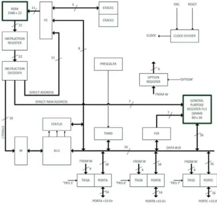
more room to maneuver during program execution. In a low-end microcontroller, the status register does not consist any overflow (OV) flag because of the overall specification of the processor does not require any operation that involves overflow of data. On the other hand, OV flag is vital in any DSP calculation thus the bit is added in the status register. OV flag will function when overflow occurred especially during accumulate operation in multiply-accumulate instruction.Figure 1 shows the completed modification of the 8-bit processor to 16-bit processor configuration.
Fig. 1: Block Diagram of UTeMRISC03
In RISC architecture, multiplication and division operation are executed by combining several basic instruction such as add and shift in order to produce the results. Consequently, this method leads to higher clock cycle to complete the operations. Therefore, a new instruction set is created to perform MAC operation in a single clock cycle. The MAC instruction set is defined by altering the operation sequences inside the RISC processor architecture.
The multiply-accumulate (MAC) unit is a common digital block used extensively in microprocessors and digital signal processors for data-intensive applications. Many filters, orthogonal frequency division multiplexing algorithms and channel estimators require FIR or FFT/IFFT computations that MAC units can accelerate efficiently. A basic MAC architecture consists of a multiplier and an accumulate adder. Inputs are fed to the multiplier and successive products are summed by the accumulate adder.
Instruction Set Generation:
The basic 8-bit processor architecture utilized a 12-bit instruction code that consists of opcode and its respective operands. The opcode occupied 6 bits at the MSB side of the ISA. Each opcode is uniquely assigned to each instruction set. The operand is made up of literal value, memory/register address or register bit which is determined by the instruction set configuration.
To form a 16-bit processor, the data bus has to be expanded to a 16-bit width. In turn, the ISA also has to be modified in accordance to the changes. For the new instructions, the ISA is expanded to a width of 22-bit in total; with the opcodes fixed to 6-bit. The clear segregation of the opcode and the operand bits is proposed to simplify the instruction decoding process. Accordingly, there are a total of 64 unique instructions that could be declared in the modified RISC architecture, although not all will be utilized at this moment.
However, memory ad
Fig. 2: Mo
The in byte-opera register loc result coul 12 bits is u instruction the 4-bit ‘b the 16-bit instruction Instruction
A CP architectur users to de the architec multiply-ac In CP constants e width are s the program
All IS to identify CPUSim’s ISA are ap the register code is 22 Each i series of op function. T assist in de pre-defined CPUS input text f array. From the correct program in instruction After s The listing have been operands i implement Assembly F
To co suitable du
if more memo ddresses. The n
odified Instruct nstruction sets and operation, b
cation and the d be either wo used to point to n set in this form
b’ is able to as available in t n address for th
n Set Simulatio PU simulation re together wit
efine CPU's ar cture. An assem ccumulate ope PUSim, all the
equivalent are setup to enable m.
A format is de the type of ins Machine Inst pplied referring
r addressing bi bits.
instruction nee perations calle The microinstr efining the ins d microinstruct Sim also provid file. All instruc m there, the pr t operations and
n order to com n sets.
successfully co g file includes i
re-programme in the hexade tation phase.
File Converter ompile all the ue to the opco
ory is required new ISA is as s
tion Set Archite are divided int bit-operand op
one output di rking register ( o the file regist mat is focusing ssign all the 16 the ISA forma he program cou
on:
tool called C th the assembl rchitecture at th
mbly program ration between e hardware m initiated as the e users to freel eclared as the i struction, the m
ruction modul g to its respecti
its could have eds to be conf d microinstruc ructions are div struction set op
tion as a refere des the capabil ctions in the as rogram is debu
d data transfers mprehend and ompleted the si instruction cod ed with the new ecimal format.
r:
programming ode incompatib
d, the ISA cou shown in Figur
ecture (ISA) to three forma eration and lite irection bit wh
(denote as 0) o ter or the mem g on single bit 6 bits of a regi at (labeled as unter use in GO
CPUSim (Skri ly program. Es he microcode
is created, whi n two sets of da odules such a e basis of the R ly configure th instruction regi memory addres es are utilized ive instruction a mixture betw figured individ ctions are assig vided into few peration. Users ence point and lity to assembl ssembly file ar ugged and all r
s. It is importan d understand t
imulation, a lis de and its memo w ISA format, t
The listing f
g codes, off-th bility with the
uld be extend re 2.
ats in order to e eral/control op hich is assigned
or back to the f mory address. In
changes, point ister file. Final ‘k’) to indica OTO and CALL
ien, 2001) is ssentially, the level and to s ich incorporate ata.
as special fun RISC architect he instructions ister (IR) and w ss or literal valu d to define the n set categories ween 12- or 16-dually before t gned for each in w categories su
s are also able subsequently r le, load and de re decoded to i elated registers nt at this stage the operationa sting file is gen
ory address loc the listing file file will then
he-shelf assem e new instructi
ed further to
easily identify eration. Byte-o d as ‘d’. Bit ‘d file register itse n bit-operand o ted by bit ‘b’. lly, literal/cont ate a literal h L instruction.
utilized to si CPUSim is a imulate the as es the new instr
ction registers ture. Program space and also would be the f ue and also the general instruc s. While the op
-bit wide with the debugging nstruction in or uch as arithmet to create cust realizing the ne ebug an assem its hexadecima s and memory to successfully al flow especia nerated based o cation. As all in
reflects the new act as the in
mblers or any ion sets. Thus
accommodate
its main opera operand operat d’ indicates tha elf (denote as 1 operation, the As the data bu trol operation m
exadecimal va
imulate the un a Java applicat
sembly-langua ruction sets, to s, memory arr Counter (PC) o memory add first point of re e directional or ction set forma pcodes are mai
the total numb process can b rder to execute tic, logic, test tom microinstr ew custom inst mbly program d al form and sto array are obse y simulate and ally for the n on the assembl nstruction sets w opcodes and nput file durin
third-party co , a customizab
all the possib
ations. There a tion involves fi at thedestinatio 1). The availab
execution of th us is 16-bit wid
makes use of a alue or the ne
nderlying RIS tion that enabl age programs o o perform a bas
rays, stacks an and address bu dress available
eference in ord r the affected b at. Variations intained as 6-b ber of instructio be performed. e the command and transfers ruction using th
truction set. designated at th ored to the RA
erved to valida d validate the te new or modifie
led test program s in the simulat d their respectiv ng the hardwa
Aust. J. Basic & Appl. Sci., 7(6): 678-687, 2013
682
developed to compile all the instruction set including the new instruction commands. The assembler is responsible to decode all the instruction in the assembly language file (*.asm) to the machine language which is in the hexadecimal format. Based on the ISA established in the previous section, all the decoding and conversion processes are done line-by-line and the decoded instructions are stored as a separate hexadecimal file.
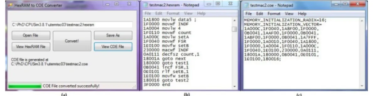
A file converter program is developed to convert the listing file generated from CPUSim to the coefficient file (*.COE). During the implementation of the RISC processor in the FPGA, all the program codes are resided in a ROM module. The ROM instantiation process requires the listing file generated by the assembler as the initialization file. However, modification and reformatting need to be done to the listing file to match the initialization file format. This process is automatically executed by the file converter module once the listing file is generated. The listing file is then renamed as the coefficient file. The coefficient file format together with the file converter interface is shown in Figure 3.
Fig. 3: (a) Graphic Interface of UTeMRISC03 Assembler (b) Sample of Test Program (c) The Coefficient File’s Format
FPGA Implementation:
The FPGA implementation is done by using Spartan-3AN FPGA board. Spartan-3AN contains 700,000 system gates, which is equivalent to 13,248 logic cells that are considered more than adequate to house the processor core design together with its memory modules and other external peripheral core such as the integrated logic analyzer (ILA). Once the COE file is initiated during the ROM module instantiation through CoreGen, the ROM module is attached to the CPU module of the UTeMRISC03 processor. All the instructions will be fetched from the ROM module and decoded in the Instruction Decoder module before being executed by the CPU. Meanwhile, the RAM module is also initiated for the purpose of storing data for the special function registers and also for the general purpose registers.
The standard processes to generate the bit stream are as shown in Figure 4. The processes include synthesis, translate, mapping, placement and route. In the placement process, the processor’s I/O pins are assigned to their respective pin in the Virtex-6 FPGA layout in a file called User Constraint File (*.ucf).
Architectural Design Simulation:
The evaluation of the output of the processor core is executed in two stages of debugging process. The first stage involved behavioral simulation on the processor architecture. Behavioral simulation provides a high level abstraction of the processor core using a pre-synthesis HDL description of the design. At this stage, the syntaxand functionality of the modules could be verified without the timing information. Therefore, errors identified during the behavioral simulation are easily rectified at an early design cycle. Subsequently, the second stage would implement the processor core on the FPGA chip and all the signals are evaluated through the Chipscope Pro program.
The ChipScope Pro ILA is an internal core embedded to the processor design that simplifies the observation of any internal signals of the design. The ILA core also includes many advanced features of modern logic analyzers, including Boolean trigger equations, trigger sequences, and storage qualification.
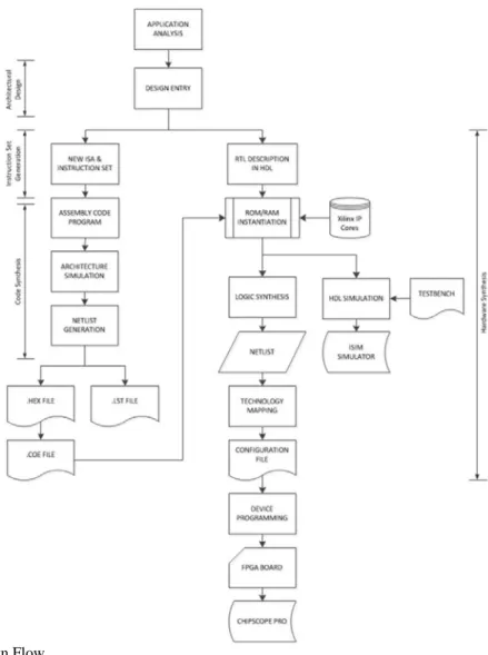
Fig. 4: ASIP Design Flow
RESULTS AND DISCUSSION
Instruction Set Generation:
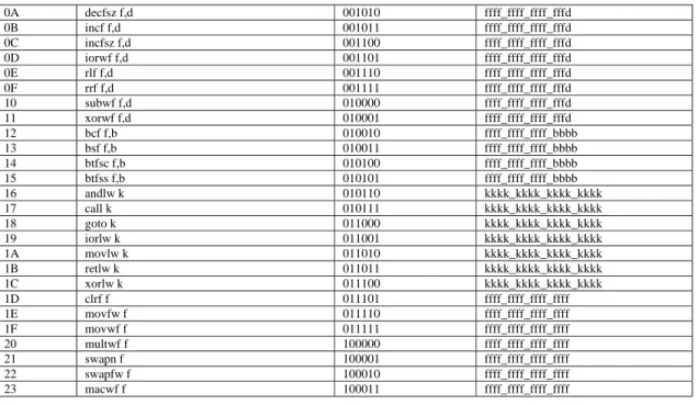
The basic 8-bit RISC processor has a total of 33 instruction sets that catered for the basic operation of the processor. However, to extend the processor’s capability in executing multiply-accumulate operations, at least two additional instruction sets are needed to perform the MAC command. Therefore, multwf and macwf instruction sets are generated and their operation is defined clearly in the ALU module.
Adopting the new 22-bit ISA format, all the original instruction sets are given new and specific instruction opcodes and operands including the newly generated instruction sets. Modifications are also being done towards the existing instruction sets so as to improve efficiency. The list of instruction sets on the UTeMRISC03 processor is as shown in Table 1.
Table 1: Complete Instruction Sets for UTeMRISC03
Opcode Instruction 22-bit opcode
6-bit 16-bit
00 nop 000000 0000_0000_0000_0000
01 clrwdt 000001 0000_0000_0000_0000
02 clrw 000010 0000_0000_0000_0000
03 option 000011 0000_0000_0000_0000
04 sleep 000100 0000_0000_0000_0000
05 tris f 000101 0000_0000_0000_0000
06 addwf f,d 000110 ffff_ffff_ffff_fffd
07 andwf f,d 000111 ffff_ffff_ffff_fffd
08 comf f,d 001000 ffff_ffff_ffff_fffd
Aust. J. Basic & Appl. Sci., 7(6): 678-687, 2013
684
0A decfsz f,d 001010 ffff_ffff_ffff_fffd
0B incf f,d 001011 ffff_ffff_ffff_fffd
0C incfsz f,d 001100 ffff_ffff_ffff_fffd
0D iorwf f,d 001101 ffff_ffff_ffff_fffd
0E rlf f,d 001110 ffff_ffff_ffff_fffd
0F rrf f,d 001111 ffff_ffff_ffff_fffd
10 subwf f,d 010000 ffff_ffff_ffff_fffd
11 xorwf f,d 010001 ffff_ffff_ffff_fffd
12 bcf f,b 010010 ffff_ffff_ffff_bbbb
13 bsf f,b 010011 ffff_ffff_ffff_bbbb
14 btfsc f,b 010100 ffff_ffff_ffff_bbbb
15 btfss f,b 010101 ffff_ffff_ffff_bbbb
16 andlw k 010110 kkkk_kkkk_kkkk_kkkk
17 call k 010111 kkkk_kkkk_kkkk_kkkk
18 goto k 011000 kkkk_kkkk_kkkk_kkkk
19 iorlw k 011001 kkkk_kkkk_kkkk_kkkk
1A movlw k 011010 kkkk_kkkk_kkkk_kkkk
1B retlw k 011011 kkkk_kkkk_kkkk_kkkk
1C xorlw k 011100 kkkk_kkkk_kkkk_kkkk
1D clrf f 011101 ffff_ffff_ffff_ffff
1E movfw f 011110 ffff_ffff_ffff_ffff
1F movwf f 011111 ffff_ffff_ffff_ffff
20 multwf f 100000 ffff_ffff_ffff_ffff
21 swapn f 100001 ffff_ffff_ffff_ffff
22 swapfw f 100010 ffff_ffff_ffff_ffff
23 macwf f 100011 ffff_ffff_ffff_ffff
Code Synthesis:
A test program is developed in assembly language that would assess the new MAC instruction set operation. Initially, two sets of input data are stored in the RAM array at different location. The test program would take the first data from each of the sets and perform multiply-accumulate operations on those data. The MAC result is stored in a special register called ‘accu_old’. This loop is repeated for the subsequent data from each of the sets. The ‘accu_old’ register is constantly being updated with new value when MAC instruction set is executed. A loop counter is utilized to limit the number of iteration according to the available data in the data sets. Figure 5 shows the debugging mode in CPUSim where the test program is executed and debugged.
Fig. 5: CPUSim Simulation
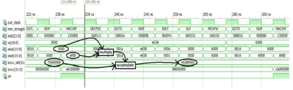
data (with four 16-bit data in each set) is stored in two separate locations, which starts at address 12 for set A and address 16 for set B. During the MAC instruction execution, the data from set A (AF0016) is fetched indirectly using the File Select Register (FSR) while data from set B (300016) is loaded to the working register. After signed-number multiply calculation is completed, the 32-bit result (F0D0_000016) is stored first in a register called ‘accnew’. Afterward, accumulate calculation is performed between the ‘accnew’ and the ‘accold’ register, which contained the MAC results from the previous MAC iteration (F568_000016). The accumulate result (E638_00016) is stored back to the ‘accold’ register to be used for the next MAC iteration. The number of iterations is controlled by setting a loop counter that depends on the number of data available in each data set. Hardware Synthesis:
After the successful verification of the new instruction set generation in the CPUSim, the core processor architecture is adopted using HDL in the Xilinx ISE Design Suite. Figure 6 shows the behavioral simulation conducted on the UTeMRISC03 processor. In Figure 6, the ‘alua’ and ‘alub’ register indicate the multiplier and multiplicand of ALU module before the MAC operation. The simulation result clearly validates the outcome from the CPUSim simulation whereby the ‘accu_old’ register are constantly updated when the MAC instruction set is executed.
Fig. 6: ISim Simulation Results
To observe the hardware execution of the processor design, the ILA core is setup to monitor 8 internal signals, matching the signals made during behavioral simulation process. Once the bitstream file is generated, the processor core is programmed to the FPGA. Figure 7 shows the results taken from Chipscope Pro Analyzer windows.
Fig. 7:ChipScope Logic Analyzer Results
The ILA results shown in Figure 7 indicated that the MAC instruction set is executed accordingly. In this instance, MAC instruction execution involved data 600016 and BF0016 as multiplier and multiplicand respectively. Once multiplication process is done (E7A0_000016), the multiplication result is accumulated with the previous accumulator value (A55B_C00016), the result (8CFB_C00016) is stored back to the ‘accu_old’ register. All MAC instruction set is executed in one clock cycle.
Aust. J. Basic & Appl. Sci., 7(6): 678-687, 2013
686
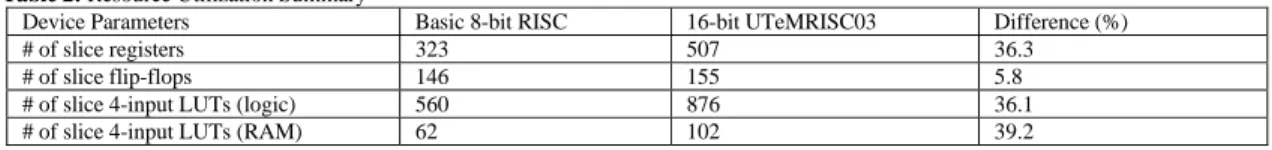
Table 2: Resource Utilization Summary
Device Parameters Basic 8-bit RISC 16-bit UTeMRISC03 Difference (%)
# of slice registers 323 507 36.3
# of slice flip-flops 146 155 5.8
# of slice 4-input LUTs (logic) 560 876 36.1
# of slice 4-input LUTs (RAM) 62 102 39.2
The expansion of data bus from an 8-bit to a 16-bit has contributed to the increased on the resource utilization as it also affected all the data registers and the memory width. However, the execution of the test program is significantly faster using UTeMRISC03 due to its less overhead and the capability in handling 16-bit multiplication compared to the 8-bit data bus limitation on its predecessor.
Conclusion:
The successful execution of multiply-accumulate operation on 16-bit RISC processor such as UTeMRISC03 processor has provided the base platform in implementing DSP operations on low-end RISC processor. Based on ASIP methodologies, new instruction sets are generated through partial customization technique and ISA modification. Having a soft-core RISC processor also aided during the design process whereby the core architecture is customized through HDL programming and validated directly via simulation and FPGA implementation. Further extensive test on the processor architecture on advanced DSP operation will be conducted in the near future to identify the processor’s limitation in handling complex arithmetic calculation.
ACKNOWLEDGMENT
The authors would like to thank Universiti Teknikal Malaysia Melaka (UTeM) and Ministry of Higher Education Malaysia for the financial support given through the research grant number FRGS/2012/FKEKK/TK02/02/1/F00126.
REFERENCES
Ball, J., 2007. Designing Soft-Core Processors for FPGAs Processor Design, In Processor Design: System-on-Chip Computing for ASICs and FPGAs, 1st ed., Nurmi, J. Springer Netherlands, pp: 229-256.
Barthe, L., L.V. Cargnini, P. Benoit, L. Torres, 2011. The SecretBlaze: A Configurable and Cost-Effective Open-Source Soft-Core Processor. In the Proceedings of the IEEE International Symposium on Parallel and Distributed Processing Workshops and Phd Forum (IPDPSW), pp: 310-313
Biswas, P., N.D.
Dutt, 2005. Code size reduction in heterogeneous-connectivity-based DSPs using instruction set extensions. IEEE Transactions on Computers, 54(10): 1216-1226.
Galuzzi, C., K. Bertels, 2011. The Instruction-Set Extension Problem: A Survey. ACM Trans Reconfigurable Technol. Syst., 4(2): 1-28.
Good, T., M. Benaissa, 2006. Very small FPGA application-specific instruction processor for AES. IEEE Transactions on Circuits and Systems I: Regular Papers, 53(7): 1477-1486.
Guan, X., 2011. Application-specific Instruction Set Processor Design for Data-intensive Applications, Ph.D. thesis, University of Connecticut, Connecticut, USA
Guan, X., Y. Fei, H. Lin, 2012. Hierarchical Design of an Application-Specific Instruction Set Processor for High-Throughput and Scalable FFT Processing. IEEE Transactions on Very Large Scale Integration (VLSI) Systems, 20(3): 551-563.
Hoffmann, A., T. Kogel, A. Nohl, G.
Braun, O. Schliebusch, O. Wahlen, A. Wieferink, H. Meyr, 2001. A novel methodology for the design of application-specific instruction-set processors (ASIPs) using a machine description language. IEEE Transactions on Computer-Aided Design of Integrated Circuits and Systems, 20(11): 1338-1354.
Hong, P.J., N. Sulaiman, 2010. Genetic Algorithm optimization for coefficient of FFT processor. Australian Journal of Basic and Applied Sciences, 4(9): 4184-4192.
Jin-Hyuk, Y., K. Byoung-Woon, N. Sang-Joon, K. Young-Su, L. Dae-Hyun, L. Jong-Yeol, H. Chan-Soo, L. Yong-Hoon, H. Seung-Ho, P. In-Cheol, K. Chong-Min, 2000. MetaCore: an application-specific programmable DSP development system. IEEE Transactions on Very Large Scale Integration (VLSI) Systems, 8(2): 173-183.
Lin, H., 2011. Multi-objective Application-specific Instruction set Processor Design: Towards High Performance, Energy-efficient, and Secure Embedded Systems, Ph.D. thesis, University of Connecticut, Connecticut, USA
Mooney, J., A.E. Mahdi, M. Halton, 2012. Application-Specific Instruction-Set Processor for Control of Multi-Rail DC-DC Converter Systems. IEEE Transactions on Circuits and Systems I: Regular Papers, (99): 1-1.
motion estimation in video applications. IEEE Transactions on Circuits and Systems for Video Technology, 15(4): 508-527.
Sahoolizadeh, H., A. Keshavarz, 2010. A FPGA implementation of neural/wavelet face detection system. Australian Journal of Basic and Applied Sciences, 4(3): 379-388.
Salim, A.J., S.I.M. Salim, N.R. Samsudin, S. Yewguan, 2012. Customized instruction set simulation for soft-core RISC processor. In the Proceedings of the IEEE Control and System Graduate Research Colloquium (ICSGRC), pp: 38-42.
Shengqi, Y., W. Wolf, N. Vijaykrishnan, 2005. Power and Performance Analysis of Motion Estimation Based on Hardware and Software Realizations. IEEE Transactions on Computers, 54(6): 714-726.
Skrien, D., 2001. CPU Sim 3.1: A Tool for Simulating Computer Architectures for Computer Organization Classes. Journal on Educational Resources in Computing (JERIC), 1(4): 46-59.
Zhaohui, L., K. Dickson, J.V. McCanny, 2005. Application-specific instruction set processor for SoC implementation of modern signal processing algorithms. IEEE Transactions on Circuits and Systems I: Regular Papers, 52(4): 755-765.