Technology (IJRASET)
©IJRASET: All Rights are Reserved
420
Bare PCB Inspection and Sorting System
Divya C Thomas1, Jeetendra R Bhandankar2, Devendra Sutar3
1
,3Electronics and Telecommunication Department, Goa College of Engineering, Ponda, Goa, India
2
Micro- Interconnecxion Pvt Ltd, Corlim, Goa, India
Abstract: This paper proposes a bare PCB inspection system using image analysis wherein the inspection algorithm mainly focuses on the defect detection and finding the exact location of the defect using the real PCB images. In this project, we have built a MATLAB program to detect bare PCB faults and the results are properly shown on a MATLAB GUI. This paper proposes a system that reduces the flaws in defect detection using JIG tool and by human visual inspection. MATLAB image processing algorithms combined with Arduino based hardware provides a low cost and efficient solution for segregating between good and defective bare PCBs.
Keywords: Arduino controller, Image Subtraction, MATLAB, PCB (Printed Circuit Board), Defect detection
I. INTRODUCTION
Printed circuit board mechanically supports as well as electrically connects electronic components through its conductive and non- conductive layers in the design. PCB defect detection has great importance in the PCB manufacturing process. Human visual inspection is the traditional way to inspect any defect in PCB but it is time consuming, tedious to workers as well as highly prone to errors due to human factors.
In the current process found, the bare PCB testing is carried out using jig tool wherein connection between specific points are tested for short and open circuit. The output of the test indicates whether the PCB is faulty or not and test points between tracks where it is shorted or open. If found faulty then the bare PCB is visually inspected to find the type of fault. This process does not help us to exactly locate where the fault is present.
This paper proposes a system which can classify between defective or non- defective PCB and show the exact location of the fault. PCB inspection using image analysis can overcome the disadvantages of human inspection in case of weariness, slowness and high cost. The advent of new electronic component fabrication technologies have made PCB design complex and compact which causes difficulties to human inspection process thus increasing inspection duration. Therefore, an automated PCB inspection system can be implemented that provides real time analysis of the bare PCB panels. In this paper we discuss a non-contact reference based image processing approach for defect detection and classification. A template of a defect free reference PCB image and a test PCB image are compared with each other using image subtraction and other procedures.
II. BAREPCBDEFECTS
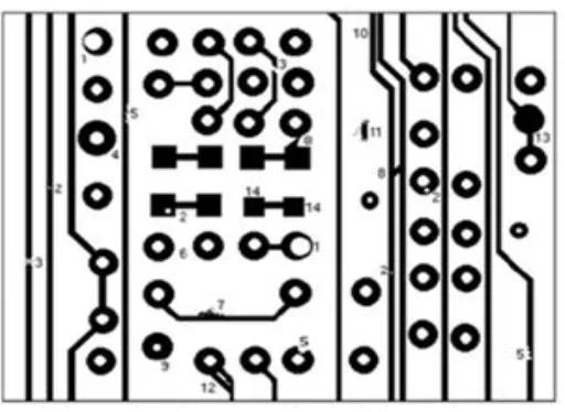
[image:2.612.198.454.544.731.2][2]There are 14 known types of defects for single layer, bare PCBs
Technology (IJRASET)
TABLEI
LIST OF BARE PCB DEFECTS
Sr.No. Defects
1 Breakout
2 Pin Hole
3 Open Circuit
4 Under Etch
5 Mouse Bite
6 Missing Conductor
7 Spur
8 Short
9 Wrong Size Hole
10 Conductor too close
11 Spurious Copper
12 Excessive Short
13 Missing Hole
14 Over Etch
III. METHODOLOGY
This paper shows the method to automate the visual inspection and sorting of bare PCB into defective and non- defective by image analysis using image processing tools. [4]This system is based on referential approach that has to be implemented on defected PCB and template images in order to detect number of defects present on bare PCB. The project aims to find out the exact location of the defect on the PCB image by color differentiation to differentiate between short and open circuit.
A. Overview
Two images are needed for the inspection, the reference image and the test image. These images are captured from the reference and test PCB laminate using a high-resolution camera. Hardware based on Arduino controller is designed to tackle problems such as misalignment of PCB, height at which the images are captured and images with bad illumination conditions and it sorts between good and bad PCBs.
Pre-processing of the image is done for obtaining accurate images which includes processes such as Image enhancement and Thresholding. Thresholding converts a gray scale image into a binary image for separation of objects of interest from the background so that further processing becomes easy. Image subtraction operation is performed between the reference image and the test image in order to point out differences between them. The resultant image shows all the defects differentiated by pseudo-coloring and displayed on the GUI.
[image:3.612.235.379.106.334.2]B. Defect Detection Algorithm
Technology (IJRASET)
©IJRASET: All Rights are Reserved
422
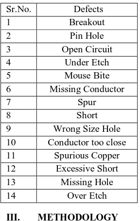
[image:4.612.189.443.99.268.2]1) Hardware for PCB Sorting System:
Fig. 3 Hardware Sorting Setup
Fig. 4 Block diagram of Hardware Sorting Setup
The proposed system requires the image capturing process to be very accurate without any problems such as misalignment, bad illumination or different heights at which the test and reference PCB images are captured. To tackle these issues, a hardware setup is made which is programmed using Arduino controller. Arduino controller is connected to the following components:
a) Power Supply: A 12V adapter is used to provide power supply to the Arduinoas well as other peripherals.
b) MATLAB PC: PC with MATLAB Program is used to analyze and find defects in PCB under Test and coordinate the result as
good or bad PCB to Arduino via Serial Communication. Program uploaded in Arduino will then drop the PCB at different depending upon the command send by MATLAB.
c) Motor Driver Circuit: L293D IC is used to drive 2 motors, one servo motor and a dc motor. The servomotor is used to rotate
the tray holding the PCB so that it can held at different positions for capturing image and after processing good and bad PCBs are dropped at 2 different positions. The dc motor is used to move the tray in and out in order to grab the PCB from the stack, to hold the PCB in the camera chamber for image capturing under good light conditions and to push the good and bad PCBs out at different positions.
[image:4.612.179.413.311.507.2]Technology (IJRASET)
coils. Hooks are used to grab the PCB from the stack and push the good and bad PCBs to different boxes.
2) Image Acquisition: [2] The process of selecting or capturing the image and giving it to system as an input is called image acquisition. Quality of the acquired image is one of key feature that depends on camera. When the camera devices are determined, it is crucial to provide proper illumination conditions to ensure image quality. Other factors such as orientation of the PCB and the height at which image is captured are considered for obtaining proper test and reference images by designing a proper hardware as discussed above. Images captured by camera are in RGB format which has to be converted to gray scale for image enhancement and further processing.
3) Image Preprocessing: Pre-processing of image is the most important step to increase accuracy of total processing procedure.
The next step in image pre-processing is image enhancement using Histogram Equalization to sharpen the edges followed by thresholding.
[2] Thresholding is a method to convert a gray scale image into a binary image so that objects of interest are separated from the back ground. [2] Thresholding algorithm involves simply setting all pixel values to a value of 0 or 1 depending on whether the gray level at each pixel is greater than or less than a threshold. Filtering of the test and binary images are done to avoid unwanted noise. Binary test image is ready for image subtraction algorithm. Binary template image is dilated according to the required tolerance so that some amount of extra copper is tolerable.
4)Image Subtraction: Image subtraction operation is performed in order to get the differences between two images that are the reference image and the inspected image. [2]The method compares both images pixel-by-pixel using XOR logic operator wherein 1 represents white pixel and 0 represents black pixel in a binary image thus the resulting image obtained contains defects. [2]The subtraction operation will produce negative and positive image. Positive image is obtained by subtracting the test image from the reference image and negative image is the result of subtracting the reference image from the test image.
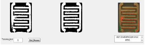
5)Fault Detection: Open circuits or cuts in the PCB shown by positive image and short circuits or extra copper in the PCB shown by negative image are superimposed on the original reference image by pseudo-coloring in order to differentiate the faults and find the exact location of fault. This image is then displayed on the GUI created and an error message will indicate the type of fault.
IV. RESULTS
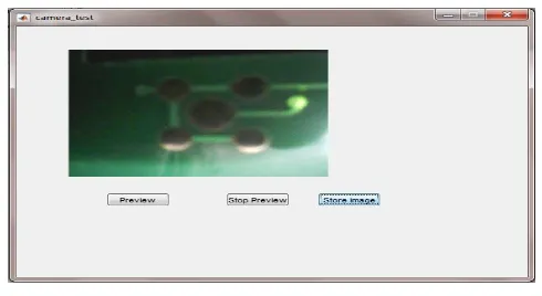
A. Capturing the PCB Image
[image:5.612.199.444.505.639.2]GUI is created to capture the image and store in the database. Here the camera connected to the PC will start the preview after clicking ’Preview’ button and stop the preview once the desired image is obtained by clicking ’stop preview’ button. By selecting on ’store image’ pushbutton the image will be stored in the Matlab database.
Fig. 5 GUI for capturing image
B. Fault Detection
Technology (IJRASET)
©IJRASET: All Rights are Reserved
424
obtain positive and negative images. These images are then superimposed on the original rgb reference image to obtain the exact location of fault. An error message is displayed on textbox on the GUI specifying whether there is short or open circuit error or there is no fault. [image:6.612.197.443.120.197.2]
Fig. 6 GUI for fault detection
V. CONCLUSIONS
This paper shows an automated bare PCB inspection system for detecting defects by image analysis. While implementing the system, we need to consider many issues that can arise and make careful plans for each step such as image acquisition, image preprocessing, image subtraction and defect recognition. Hardware setup can solve the common problems that arise as discussed. At present, the finished PCB inspection system can detect common PCB defects such as: short circuit, open circuit in real time images. After images have been acquired, thresholding, noise filtering and image subtraction operations are used to get noise-free positive and negative images which are then superimposed on the original reference image by pseudo-coloring to obtain the exact location of the defect. In this system, the results are displayed on Matlab GUI thus the user can load the image and start the processing on it by selecting given graphical elements such as pushbuttons for it. Also GUI is very simple to use as it does not need more experience or training to use. Human visual inspection of the resultant image with defects superimposed on GUI can determine whether the PCBs can be rectified or they have to be thrown out as scrap.
VI. ACKNOWLEDGMENT
I am deeply indebted to my guide, Prof. Devendra Sutar, Professor, Department of Electronics and Telecommunication Engineering, GEC and Mr. Jeetendra R Bhandankar, Senior Manager, Micro– Interconnecxion Pvt Ltd., Corlim, Goa for allowing me to carry out this project under her supervision. He has given me confidence to take up this project and guided me at times of difficulty.
I thank my teachers, who have taught enthusiastically at the Goa College of Engineering. I also thank Dr. Hassanali Virani, (Head of the Department), Department of Electronics and Telecommunication Engineering and Dr. Vinayak N. Shet (Principal) Goa College of Engineering for allowing me to do this project and providing the necessary infrastructure.
I thank my parents, family members and well-wishers, without whom this project would not have taken shape.
REFERENCES
[1] International Journal of Engineering and Innovative Technology (IJEIT) Volume 4, Issue 11, May 2015 188
[2] ‘A Review of PCB Defect Detection Using Image Processing’, International Journal of Science, Engineering and Technology Research (IJSETR) Volume 4,
Issue 4, April 2015 ,1. Anoop K.P, 2. Sarath N.S, 3. Sasi Kumar V. V.
[3] ‘PCB INSPECTION SYSTEM USING IMAGE PROCESSING’, International Conference on Computing,Communication and Automation (ICCCA2015)
2015 IEEE 11, 1. Namita Kalyan Shinde, 2. Prof.S.S.Morade
[4] ’A Novel Approach of Standard Data Base Generation for Defect Detection in Bare PCB’, International Journal of Innovative Research in Science,
Engineering and Technology Vol. 5, Issue 6, June 2016 1. Mukesh Kumar, 2. Niraj Kumar Singh, 3. Manjesh kumar,4. Ajay kumar Vishwakarma
[5] ‘PCB Fault Detection by Image Processing Tools: A Review’, International Journal of Emerging Research in Management &Technology (Volume-3, Issue-8)
1. Akash Kasturkar, 2. Dr.S. D. Lokhande
[6] Detection and Classification of Printed Circuit Board Defects Using Image Subtraction Method 1. Beant Kaur, 2. Gurmeet Kaur, 3. Amandeep Kaur