ISSN Online: 2162-5328 ISSN Print: 2162-531X
Power Law Nature in Electron Solid Interaction
Moirangthem Shubhakanta Singh
1, R. K. Brojen Singh
2*1Department of Physics, Manipur University, Canchipur, India
2School of Computational and Integrative Sciences, Jawaharlal Nehru University, New Delhi, India
Abstract
Monte Carlo simulation of paths of a large number of impinging electrons in a multi-layered solid allows defining area of spreading electrons (A) to cap-ture overall behavior of the solid. This parameter “A” follows power law with electron energy. Furthermore, change in critical energies, which are minimum energies loses corresponding to various electrons, as a function of variation in lateral distance also follows power law nature. This power law behavior could be an indicator of how strong self-organization a solid has which may be used in monitoring efficiency of device fabrication.
Keywords
Monte Carlo Simulations, Power Law, E-Beam Lithography, Electron Solid Interaction
1. Introduction
The interaction of beam of energetic electrons with the target solid material technique, which is electron beam lithography, is of great interest in probing material properties (chemical, electrical, physical etc.) [1] at sub-micron and nanoscale level [2], and has many applications, modeling radio-induced cellular damages [3], in surface science technology [4], nanolithography techniques [5], fabrication of fractal surfaces [6], various biological applications [7] etc. The im-pinging energetic electron suffers random collisions from a number of scattering centres with random distribution of potentials in the centres in the solid mate-rials of various layers [3], and the electron follows a stochastic path inside the solid material [1]. The analysis of the electron paths could highlight some of the important properties of the material which will be used in various device fabri-cations and various other applifabri-cations.
One of the most important properties of real networks, ranging from social to biological protein-protein networks [8], is power law nature of the network dis-How to cite this paper: Singh, M.S. and
Singh, R.K.B. (2017) Power Law Nature in Electron Solid Interaction. Advances in Materials Physics and Chemistry, 7, 11-18. http://dx.doi.org/10.4236/ampc.2017.71002
Received: December 6, 2016 Accepted: January 19, 2017 Published: January 22, 2017
Copyright © 2017 by authors and Scientific Research Publishing Inc. This work is licensed under the Creative Commons Attribution International License (CC BY 4.0).
tribution [9] which could be a reflection of fractal nature of the system [10]. Since fractal behavior of the system can be used as an indicator of self-organization in the system [11], one can use this property to identify important patterns and their origin in the system [12] [13] [14]. The path of the penetrating electrons in solid system is the reflection of organization of the regular scattering centres with random potential distributions; one can identify probable parameters to capture patterns of organization in the solid material. In this work, we try to search for possible parameters to characterize fractal nature of the solid systems using Monte carlo simulation procedure which could be used for various fabri-cation techniques. In Section 2, the detailed Monte Carlo procedure of electron- solid interaction is described. Simulation results are described in Section 3, and some conclusions are drawn based on the simulation results.
2. Electron Solid Interaction Model
The path traversed by impinging energetic electrons in solid is based on the electron transport within the stochastic formalism of scattering process of elec-trons with the solid along their trajectory [3] [15]. The penetrating electrons en-counter randomly distributed scattering centres within the electron interaction range [3], and the electrons undergo complicated Brownian paths inside the solid [16]. These electrons with energy (E) move in straight lines between any two scattering centres, and once they suffer interaction with scattering centres of the solid, the change in their directions are defined by
(
E, ,θ φ
)
, where,θ
andφ
are scattering and azimuthal angles respectively. The solid could be single ormulti-layered thin film with different distributions of scattering centres in dif-ferent solid layers.
We consider impinging electrons suffering elastic collisions from scattering centres distributed in the single or multi-layered thin solid film, where, differen-tial cross section can be described by classical screened Rutherford’s formula
[16],
(
)
( )
4
2
1 d
dΩ 4 1 cos 2
e Z Z E
σ
θ β
+ =
+ +
(1)
where, e is electronic charge, Z is the atomic number of the material and dΩ is solid angle.
β
is screening parameter to account for electrostatic screening ofthe nucleus by the orbital electrons, and is given by Thomas-Fermi model of the atomic field [17],
0.316
β
=0 1 3
Z pa
(2)
where, a0 is Bohr radius; is Planck’s constant and p is the electron’s
momentum. The scattering angle
θ
can be calculated by evaluating total elastic cross section σ=∫
dΩ from Equation (1),( )
( )
( )
1 1 1 2
1
cos F
F
β θ θ
θ β
− + +
=
+
where, F
( )
θ
is accumulated function of scattering probability [18] which is afunction of theta only. In the Monte Carlo simulation procedure,
θ
can be ob-tained by generating a uniform random number R1 in [0, 1], and azimuthal angleφ
by generating another uniform random number R2 and using,2
2 R
φ= π (4)
Thus,
θ
andφ
can be calculated by generating two sets of uniform randomnumbers, and using Equation (3) and (4).
2.1. Energy Loss Calculation of Traversing Electron
The energy of the electron, suffering interaction from the scattering centres dis-tributed randomly along its path, continuously loses its kinetic energy and can be calculated using Bethe’s continuous slowing down approximation model [19]. This model is a good empirical method for high energetic electrons as compared to ionization energy J i.e. for EJ, but suffers problem for E J≤ [20]. However, the model was generalized for all range of energies [21], where, the energy loss ∆E of the penetrating electron a path length L along its trajectory is given by,
0 d d d L E E z z ∆ = −
∫
(5)4 ln 1.166 and
1 d 2π
d A
N
E E J
J ME C e z C ρ ∈ ∈ + − =
where, M is the atomic weight of the target material;
ρ
is the density; NA is theAvogadro’s number and C is a constant (C→1; C < 1). The mean ionization
energy J can be obtained from the empirical formula [22],
1.19
9.76 58.8
J Z
Z
−
= + (6)
where . J 9.76
Z → as Z → ∞. Further, the sensitivity of the J in Monte Carlo
simulation can be controlled by taking logarithm of this parameter.
2.2. Modeling Electron Path in Multi-Layered System
The mean free path for single layered system, calculated using Equation (1), can be extended for multi-layered system by defining a probability Pm(u) that the
electron once scattered from first layer is not scattered until mth layer [23] [24], and can be obtained from the following Equation,
( )
( )
m d Γ d m Pm u P uu =− (7)
where, Γm is scattering probability per unit length in mth layer. Boundary condition is taken as P1
( )
0 1= . Solving Equation (7) one can arrive at(
)
( )
1
m m m
P + u u− =P u , where, um is the distance between mth and (m + 1) th
layers along z-axis. This P um
( )
can be related to F u( )
by,( )
1 m( )
1 1free path for single layer system is calculated as 1 1
( )
1 0d 1 Γ
uP u u
λ =
∫
= − , where,( )
(
)
1 1
P u =exp − Γu . Similarly, mean free path for two layered system is given by, 2 1
( )
1( )
(
2 1)
( )
10
d d 1 1 1 exp
u
u
u P u u u P u u u
λ =
∫
′ ′ ′+∞∫
′ ′ ′= Γ + Γ − Γ Γ . Proceedingin the same way, mean free path for m layered system can be calculated using,
( )
( )
( )
1 2
1 1
1 1 1
0
d d d
u u
m
u u
u P u u u P u u u P u u
λ =
∫
′ ′ ′+∫
∞ ′ ′ ′+ + ∞∫
′ ′ ′ (8)From Equation (8) one can able to calculate um of impinging electron in mth
layered material system. Now, starting from an initial vector
(
0, ,0 0)
T x y z , we can trace the path of the penetrating electron in m-layered system using the fol-lowing recursive procedure,
1 1 1 sin cos sin sin cos
n n n n
n n n n
n n n
x x y y z z θ φ θ φ θ + + + = + (9)
Thus the path of the penetrating electron in m-layered material system can be traced using the recursive procedure in (9) with average energy loss ∆E within the Monte Carlo simulation.
3. Results and Discussion
We consider single layered GaP and double layered system of GaP with resist PMMA (C5H8O2), and simulated using the Monte Carlo simulation procedure
described in the previous section to trace the trajectory of impinging energetic electrons in the systems and energy loss. The initial positions of the penetrating 500 electrons are taken as the same as
(
0, ,0 0) (
0,0,0)
T T
x y z = for a range of
energy [2 - 100] keV. The trajectory of each electron of energy E is calculated using Monte Carlo procedure (9), and energy loss (∆E) during the process of penetration is obtained using Equation (5). In our simulation the ionization energies of C, H and O are taken to be 78 eV, 18.7 eV and 89 eV, and for GaP, Equation (6) is used to calculate its J. Since the ionization energy of both GaP and PMMA are of the order of eV, EJ in our case and therefore, we take C <1in Equation (5) during the calculation. The thickness of the PMMA resist is taken to be 10−8 metre in the double layered calculation.
3.1. Power Law Nature of Electron Spreading Area
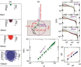
Figure 1. The plots in left panel show the trajectories of 500 electrons in single solid GaP thin film with area of spreading of electron paths (circles) for different energies 5 keV, 30 keV, 50 keV and 100 keV. The schematic diagram of impinging electrons with random scattering events is shown in upper middle panel. The plot of A versus E is shown in middle lower panel. Solid line is the fit on the data. The right panels show the plots of loss in energy as a function of lateral distance R for various energies of the electrons. The lower right panel shows the plot of ∆E versus ∆R and solid line is the fit on the data.
( )
~ gA E E (10) The straight line is the fitting curve to the calculated data. The value of
γ
is found to be 1.98.We then calculated the As in double layered material system (1 µm thickness
for PMMA and rest for GaP) for various electron energies [2 - 100] keV (Figure 2 left panels). The behavior of A with respect to E (Figure 2 middle upper panel) has three regimes, left (electrons paths are within single first layer only) and right (dominated by second layer as compared to first layer) regimes follow sim-ilar power law given by Equation (10), and the values of
γ
are found to be 2.1 and 1.97 respectively. The middle regime, which is due to contributions from both first and second layers, does not follow exact power law nature.3.2. Power Law Behaviour in Energy Loss
Figure 2. The plots in the two columns in the left panel show the trajectories of 500 elec-trons in single solid double layered system of GaP with resist PMMA thin film with area of spreading of electron paths (circles) for different energies [2 - 100] keV. The plot of A
versus E is shown in the upper right panel with different interaction regimes. Solid line is the fit on the data. The lower panels show the plots of loss in energy as a function of lat-eral distance R for various energies of the electrons. The lower right panel shows the plot of ∆E versus ∆R and solid line is the fit on the data.
Ec and Rc for different Es in the range [10 - 100] keV. Then we calculated
possi-ble changes in these critical energies (∆E) as a function of ∆R starting from lowest (Ec, Rc), and error bars are standard deviations of the thicknesses of the
drop curves (lines drawn parallel to E axis in Figure 1 right panels). The calcu-lated ∆E again follows power law with ∆R as follows,
d
E R
∆ ∼∆ (11) The power law fit to the data gives the power law exponent to be
δ
=2.21. We now calculated ∆E in double layered material system as a function ofR
∆ for energies [10 - 100] keV (Figure 2 left lower panels). Surprisingly, even though there is contributions from first and second layers, the behavior of ∆E
as a function of ∆R follows the similar power law nature as Equation (11) with the value of
δ
=2.17.4. Conclusion
The power law behavior is found to various systems, starting from social sys-tems to brain protein-protein networks which indicate important functional and organizational characteristics. This behavior indicates that the properties of the system are independent of scale of the system. Since this law also reflects the fractal nature of the system, it characterizes as an indicator of self-organized be-havior of the material system. The impinging energetic electrons experience the self-organized behavior of the system which is reflected in the parameters calcu-lated using Monte Carlo simulation procedure. This idea of fractal nature could be used as an order parameter in the fabrication of multi-layered device with proper efficiency.
References
[1] Kyser, D.F. and Viswanathan, N.S. (1975)Monte Carlo Simulation of Spatially Dis-tributed Beams in Electron-Beam Lithography. Journal of Vacuum Science and Technology, 12, 1305-1308. https://doi.org/10.1116/1.568524
[2] Zhou, Z. (2004) Electron Beam Lithography. In: Yao, N., Ed., Handbook of Micro-scopy for Nanotechnology, Kluwer/Springer.
[3] Shimizu, R. and Ding, Z.J. (1992)Monte Carlo Modelling of Electron-Solid Interac-tions. Reports on Progress in Physics, 55, 487-531.
https://doi.org/10.1088/0034-4885/55/4/002
[4] Niedrig, H. (1982) Erratum: Electron Backscattering from Thin Films [Journal of Applied Physics, 50, R15 (1982)]. Journal of Applied Physics, 53, 815.
https://doi.org/10.1063/1.331653
[5] Grigorescu, A.E. and Hagen, C.W. (2009)Resists for Sub-20-nm Electron Beam Li-thography with a Focus on HSQ: State of the Art. Nanotechnology, 20, Article ID: 292001. https://doi.org/10.1088/0957-4484/20/29/292001
[6] Stoliar, P., Calo, A., Valle, F. and Biscarini, F. (2010)Fabrication of Fractal Surfaces by Electron Beam Lithography. IEEE Transactions on Nanotechnology, 9, 229-236.
https://doi.org/10.1109/TNANO.2009.2027232
[7] Etin, A. and Ko, K. (2015) NeuroQuantology, 2, 160-169.
[8] Albert, R. and Barabasi, A. (2002)Statistical Mechanics of Complex Networks. Re-views of Modern Physics, 74, 47. https://doi.org/10.1103/RevModPhys.74.47
[9] Albert, R. and Barabasi, A. (1999) Emergence of Scaling in Random Networks.
Science, 286, 509-512. https://doi.org/10.1126/science.286.5439.509
[10] Jung, S., Kim, S. and Kahng, B. (2002)Geometric Fractal Growth Model for Scale- Free Networks. Physical Review E, 65, Article ID: 056101.
https://doi.org/10.1103/PhysRevE.65.056101
[11] Kauffman, S.A. (1993) The Origins of Order: Self-Organization and Selection in Evolution. Oxford University Press, Oxford.
[12] Mandelbrot, B.B. (1983) The Fractal Geometry of Nature. WH Freeman and Co., New York.
[13] Peitgen, H.-O., Jurgens, H. and Saupe, D. (1992) Chaos and Fractals: New Frontiers of Science. Springer, New York. https://doi.org/10.1007/978-1-4757-4740-9
[14] Theiler, J. (1990) Estimating Fractal Dimension. Journal of the Optical Society of America A, 7, 1055-1073. https://doi.org/10.1364/JOSAA.7.001055
Ad-vanced Science Letters, 3, 1-5. https://doi.org/10.1166/asl.2010.1080
[16] Murata, K. and Kyser, D.F. (1987) Monte Carlo Methods and Microlithography Simulation for Electron and X-Ray Beams. Advances Electronics and Electron Physics, 69, 175-259. https://doi.org/10.1016/S0065-2539(08)60202-4
[17] Nigam, B.P., Sunderesan, M.K. and Ta-Yu, W. (1954) Theory of Multiple Scatter-ing: Second Born Approximation and Corrections to Molière’s Work. Physical Re-view, 115, 491-502. https://doi.org/10.1103/PhysRev.115.491
[18] Tokesi, K. and Mukoyama, T. (1994) Bulletin of the Institute for Chemical Re-search, 72, 3-4.
[19] Bethe, H.A. (1933) Quantenmechanik der Ein- und Zwei-Elektronenprobleme. In: Bethe, H.A., et al., Eds., Quantentheorie, Vol. 24, Springer, Berlin, 273-560.
https://doi.org/10.1007/978-3-642-52619-0_3
[20] Rao-Sahib, T.S. and Wittry, D.B. (1974) X-Ray Continuum from Thick Elemental Targets for 10-50-keV Electrons. Journal of Applied Physics, 45, 5060-5068.
https://doi.org/10.1063/1.1663184
[21] Joy, D.C. and Luo, S. (1989) An Empirical Stopping Power Relationship for Low-Energy Electrons. Scanning, 11, 176-180.
https://doi.org/10.1002/sca.4950110404
[22] Berger, M.J. and Setzer, S.M. (1964) Studies in Penetration of Charged Particles in Matter. National Academy of Sciences, Washington DC, Chap. 10, 1133.
[23] Horiguchi, S., Suzuki, M., Kobayashhi, T., Yoshino, H., and Sakakibara, Y. (1981) New Model of Electron Free Path in Multiple Layers for Monte Carlo Simulation.
Applied Physics Letters, 39, 512-514. https://doi.org/10.1063/1.92785
[24] Hawryluk, R.J., Hawryluk, A.M. and Smith, H.I. (1982)Addendum: New Model of Electron Free Path in Multiple Layers for Monte Carlo Simulation. Journal of Ap-plied Physics, 53, 5985. https://doi.org/10.1063/1.331408
Submit or recommend next manuscript to SCIRP and we will provide best service for you:
Accepting pre-submission inquiries through Email, Facebook, LinkedIn, Twitter, etc. A wide selection of journals (inclusive of 9 subjects, more than 200 journals)
Providing 24-hour high-quality service User-friendly online submission system Fair and swift peer-review system
Efficient typesetting and proofreading procedure
Display of the result of downloads and visits, as well as the number of cited articles Maximum dissemination of your research work
![Figure 2. The plots in the two columns in the left panel show the trajectories of 500 elec-of spreading of electron paths (circles) for different energies [2 - 100] keV](https://thumb-us.123doks.com/thumbv2/123dok_us/7786347.723767/6.595.210.535.65.313/figure-columns-trajectories-spreading-electron-circles-different-energies.webp)
