PCB Defect Detection, Classification and Localization
using Mathematical Morphology and Image Processing
Tools
Malge P.S.
Department of Electronics,
Walchand Institute of Technology, Solapur.413006
Nadaf R.S.
Department of Electronics,
Walchand Institute of Technology, Solapur.413006
ABSTRACT
An automated visual printed circuit board (PCB) inspection is an approach used to counter difficulties occurred in human’s manual inspection that can eliminates subjective aspects and then provides fast, quantitative, and dimensional assessments. Various concentrated work on detection of defects on printed circuit boards (PCBs) have been done, but it is also crucial to classify these defects in order to analyze and identify the root causes of the defects. This project proposes a PCB defect detection and classification system using a morphological image segmentation algorithm and simple the image processing theories. However, besides the need to detect the defects, it is also essential to classify and locate these defects so that the source and location of these defects can be identified. Based on initial studies, some PCB defects can only exist in certain groups. Thus, it is obvious that the image processing algorithm could be improved by applying a segmentation exercise. This project uses template and test images of single layer, bare, grayscale computer generated PCBs.
Keywords
PCB panel, vision, image processing, segmentation and Image Processing.
1.
INTRODUCTION
The PCB (printed circuit board) manufacturing is becoming more and more important as the consumer electronics products, such as mobile phones, tablet PCs, automatic washing machines and so on, are indispensable for our everyday life. Visual inspection is generally the largest cost of PCB manufacturing. It is responsible for detecting both cosmetic and functional defects and attempts are often made to ensure 100% quality assurance for all finished products. There are three main processes in PCB inspection: defect detection, defect classification and defect location. Currently there are many algorithms developed for PCB defect detection and classification using contact or noncontact methods [3]. Contact method tests the connectivity of the circuit but is unable to detect major flaws in cosmetic defects such as mouse-bite or spurious copper and is very setup-sensitive [12]. Any misalignment can cause the test to fail completely.
Non contact methods can be from a wide range of selection from x-ray imaging, ultrasonic imaging, thermal imaging and optical inspection using image processing [5 - 6]. Although these techniques are successful in detecting
defects, none is able to classify the defects.In a non contact reference based, image processing approaches template of a defect free PCB image and a defected test PCB image are segmented and compared with each other using image subtraction and other procedures.
This project utilizes a non contact reference based, image processing approach for defect detection and classification and simple image processing algorithm for locating those defects on PCB board. A template of a defect free PCB image and a defected test PCB image are segmented and compared with each other using image subtraction and other procedures. Discrepancies between the images are considered defects and are classified based on similarities and area of occurrences. After obtaining patterns concerning the results these are located on the PCB. This paper is organized as follows. Section 2 defines the review of previous works and research methodology chosen for this project. Section 3 and describes the details of mathematical morphology for image segmentation and image processing algorithm for detection and classification of PCB defects. Section 4 contains the experimental results for defect detection and classification while the discussion and conclusion is described in section 5.
2.
LITERATURE REVIEW
Bare printed circuit board (PCB) is a PCB without any placement of electronic components (Hong et al., 1998) which is used along with other components to produce electrics goods. In order to reduce cost spending in manufacturing caused by the defected bare PCB, the bare PCB must be inspected. Moganti et al. (1996) proposed three categories of PCB inspection algorithms: referential approaches, non-referential approaches, and hybrid approaches.
Referential approaches consist of image comparison and model-based technique. Non-referential approaches or design-rule
verification methods are based on the verification of the general design rules that is essentially the verification of the widths of conductors and insulators.
detection did not provide satisfactory information for repairing and quality control work, since the type of detected defects cannot be clearly identified. Based on this incapability of defects detection, defect classification operation is needed in PCB inspection. Therefore, an accurate defect classification procedure is essential especially for an on-line inspection system during PCB production process.
Human operators simply inspect visually against prescribed standards. The decisions made by them often involve subjective judgment, in addition to being labor intensive and therefore costly, whereas automatic inspection systems remove the subjective aspects and provide fast, quantitative dimensional assessments. Due to the following criteria, the sophistication in automated visual inspection has become a part of the modern manufacturing environment.
They relieve human inspectors of the tedious jobs involved.
Manual inspection is slow, costly, leads to excessive scrap rates, and does not assure high quality.
Multi-layer boards are not suitable for human eyes to inspect.
With the aid of a magnifying lens, the average fault- finding rate of a human being is about90%. However, on multi-layered boards (say 6 layered), the rate drops to about 50%. Even with fault free power and ground layers, the rate does not exceed 70% [9].
Industry has set quality levels so high that sampling inspection is not applicable.
Production rates are so high that manual inspection is not feasible.
Tolerances are so tight that manual visual inspection is inadequate.
A variety of approaches for automated optical inspection of printed circuit boards (PCBs) have been reported over the last two decades.
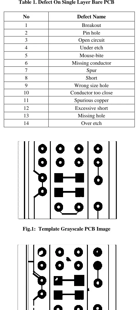
PCB defects can be categorized into two groups; functional defects and cosmetic defects [5]. Functional defects can seriously affect the performance of the PCB or cause it to fail. There are 14 known types of defects for single layer, bare PCBs as shown in Table 1. Figure 1 shows a grayscale image of a single layer, bare PCB and Figure 2 shows the same image but with defects as listed in Table 1.
Based on reviews of previous works, Heriansyah et al [1] developed a PCB image segmentation algorithm by clustering primitive patterns of a PCB image into four main segments using mathematical morphology and windowing technique. Later Heriansyah [9] classifies 12 out of the 14 known PCB defects by combining the image segmentation with artificial neural network (ANN). Recently, Khalid [2] produced an image processing algorithm using MATLAB by subtracting the images and performing X-OR operation. The 14 defects are then grouped into 5 categories.
[image:2.612.318.551.74.604.2]Table 1. Defect On Single Layer Bare PCB
[image:2.612.347.518.491.631.2]Fig.1: Template Grayscale PCB Image
Fig.2: Test Grayscale PCB Image
This project combines two previous works. First, the complex PCB images are divided into four different segments of well-defined generic patterns [1], and later fed into the image processing algorithm [2] where defects are
No Defect Name
1 Breakout
2 Pin hole
3 Open circuit
4 Under etch
5 Mouse-bite
6 Missing conductor
7 Spur
8 Short
9 Wrong size hole
10 Conductor too close
11 Spurious copper
12 Excessive short
13 Missing hole
detected and classified. Then by using these patterns we locate these patterns on defected PCB.
3. METHODOLOGY
3.1 Mathematical Morphology for Image
Segmentation
The algorithms to segment the image into basic primitive patterns, enclosing the primitive patterns, patterns assignment, patterns normalization, and classification have been developed based on binary morphological image processing.
After segmenting the PCB image into basic primitive patterns, the next step is to enclose each pattern so that only pixels under this window will be processed. Windowing operation is also employed to the detected defective patterns .The defects detection applied in this work is based on the image subtraction operation [1].
The segmented primitive patterns of the reference image will be enclosed using the windowing technique, and these window coordinates will be mapped onto the test image to generate the same window coordinates for the test image. At the same time, the detected defects from previous subtraction operation will also be enclosed using the same windowing technique.
The next step is to do the assignment operation. The aim of this assignment operation is to define the position of the enclosed defect patterns relative to the enclosed test image patterns.
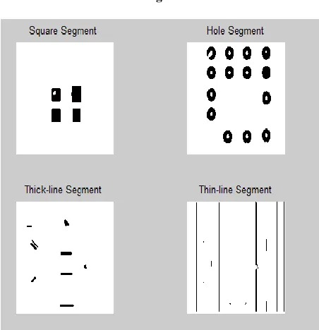
This research does an adaptation of the mathematical morphology for image segmentation by Heriansyah et al [1] in preparing the images for defect detection and classification. MA TLAB is used for this purpose. A template image is a grayscale image of a perfect PCB pattern without any defects or deformation which is used as reference as in Figure 1.
A test image is a grayscale image of a defective PCB as in Figure 2 which is synthetically generated to contain all 14 defects as listed in Table 1. Both the images are segmented into 4 segments each; square segment, hole-segment, thick-line segment and thin-thick-line segment as in Figure 3 and Figure 4. The square segment contains the image of square pads, the hole-segment contains the image of hole pads, the thick-line segment contains the image of thick conductors and the thin-line segment contains the images of thin conductors.
[image:3.612.323.544.72.244.2]Some defects only occur on particular segments of test image such as wrong size hole, breakout and missing hole for hole segment or missing conductor and open circuit for thin-line segment. Other defects might exist in multiple segments. Mouse-bite and under-etch might exist in both hole and square segments. By breaking the image into clusters, some of the defects associated with certain segments can easily be identified and classified.
Fig.3: Morphological Segmentation for Template Image
Fig.4: Morphological Segmentation for Test Image
3.2 Image Processing For PCB Defect
Detection and Classification
Once the template and test images are segmented, threshold values for the grey scale images are determined to convert the images into binary. Grey scale images with levels of between 0 and 255 are converted into binary images with only two levels; 0s and 1s. This is to simplify further processes. This project will not consider uneven binary convergence that can cause unwanted noise. It is observed that unwanted noise occurs occasionally in the thin-line and thick-line segments which can be removed by using median filtering.
[image:3.612.325.551.273.507.2]3.2.1 Image difference operation
[image:4.612.66.297.160.231.2]Image difference, which is the simplest technique, consists of comparing both images pixel-by-pixel by XOR logic operator. The operation is also called as image comparison operation. The truth table of XOR is given in Table 2.Image difference operation is developed in order to get the differences between two images.
Table 2: Truth Table of XOR Logic Operator
Bit 1 Bit 2 Output
0 0 0
0 1 1
1 0 1
1 1 0
3.2.2 NOT operator
[image:4.612.66.294.306.351.2]NOT operator is normally used to change an image from black to white and vice versa. This operator inverts the bit values of any variable and sets the corresponding bit according to Table 3.
Table 3: NOT Truth Table
Input Output
0 1
1 0
3.2.3 Flood-fill operator
The flood-fill operator changes the color of a region, given an initial pixel in that region on binary and grayscale images. For binary images, flood-fill operator changes connected background pixels to foreground pixels until it reaches object boundaries. This operation could be useful in removing irrelevant artifacts from images. In this study, this operator is used to fill the holes in a binary image.
3.2.4 Image Subtraction
Image subtraction method used the concept of simple subtraction and rule. In this work, both images of template image and defective image are compared pixel by pixel. The subtract operation produces either negative or positive pixel value. Therefore, the outcome of this operation is divided into negative image and positive image.
3.2.5 Image addition
Image addition is a method for combining objects in two images into one image. In this paper, this operator combines the defects from one group with the defects from another group in one image. This is possible using OR logic operator. Five algorithms shown in Figure 7 to Figure 11 are developed to detect and classify the defects into five groups. Those groups with the respective defects areas follow:
Group 1: missing hole and wrong size hole
Group 2: spur, short, spurious copper, excessive short, underetch negative, and conductor too close negative. Group 3: open circuit, mouse bite, overetch, conductor too close positive.
Group 4: underetch positive.
Group 5: pinhole and breakout.
The image processing algorithm produces 5 new images for each pair of segmented template and test images processed. Since the morphological segmentation algorithm is able to produce 4 images for both template and test image, thus, the image processing algorithm is able to generate 4x5 images (20 images) which will improve the overall defect detection and classification ability of the system.
3.3 Defect Location
By using defected patterns generated by above algorithm and defected PCB image we can locate those defects on PCB. Its advantage is it possible to tell where exactly defect has occurred, which not possible only seeing at defects. Function regionprops () is used for above purpose.
4.
RESULTS
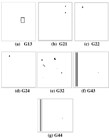
Based on exercises conducted for several test and template images, an example of result obtained is shown in Figure 5. From the 20 images generated by the image processing algorithm, 7 images were identified as beneficial. The images are named G13, G21, G22, G24, G32, G43 and G44.
(a) G13 (b) G21 (c) G22
(d) G24 (e) G32 (f) G43
(g) G44
Fig.5 (a-g): Classified Defect Images
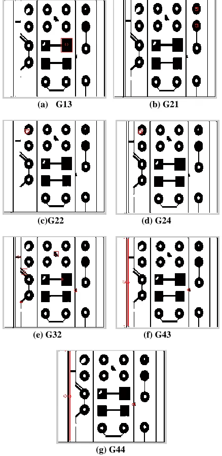
[image:4.612.323.539.359.632.2]processing algorithm by Khalid [2] by increasing the classification groups from 5 to 7.
(a) G13 (b) G21
(c)G22 (d) G24
(e) G32 (f) G43
(g) G44
Fig. 6 (a-g): Classified Defect Images
[image:5.612.71.290.94.543.2]G 13 is generated from the square segment, G21, G22 and G24 from the hole segment, G32 from the thick-line segment and G43 and G44 from the thin line segment. The defects classified by these groups are listed in Table 4. Once the overall result for classification has been obtained, the localization operating will take place so that the defect will be highlighted on the fine (original) image. The location will be superimposed on the original image with a red marker as shown in Figure 6(a-g).
Table 4:Classified Defect Groups
No. Image Defect Classified
1 G13 Under etch
2 G21 Wrong size hole
Missing hole
3 G22 Over etch
Mouse bite
4 G24 Breakout
5 G32
Short Excessive short Spurious copper
Spur
6 G43 Missing conductor
Open circuit
7 G44 Conductor too close
5.
CONCLUSION
From the above experiment, the given algorithm successfully detects and classifies defects into 7 groups. (G13, G21, G22, G24, G32, G43, G44). Due to these results, the proposed algorithm detects successfully several types the defects such as breakout, short, pin hole, wrong size hole, open circuit, conductor too close, under etch, spurious copper, mouse bite, excessive short, missing conductor, missing hole, spur and over etch. After detecting defects localization of defects makes inspection easy and precise. The limitation of this algorithm is that some groups are unable to address each defect individually. Unwanted images were also generated by noise during grayscale to binary conversion. Future improvement for the algorithm should include the ability to detect and classify all 14 defects individually.
6.
REFERENCES
[1] R. Heriansyah, S.A.R AI-Attas, and M.M. Ahmad Zabidi,'Segmentation of PCB Images into Simple Generic Patterns usingMathematical Morphology and Windowing Technique', CoGRAMMMelaka, Malaysia 2002
[2] N.K. Khalid. 'An Image Processing Approach Towards Classification of Defects on Printed Circuit Board', Projek Sarjana Muda, Universiti Teknologi Malaysia, 2007.
[3] M. Moganti, F. Ercal, C.H. Dagli, and S. Shunekawa, 'Automatic PCB Inspection Agorithm: A Survey', 1996, 63. No. 2.
[4] T. Taniguchi, D. Kacprzak, S. Yamada, M. Iwahara, and T.Miyogashi, 'Defect Detection on Printed Circuit Board by using Eddy-Current Technique and Image Processing', 101 Press, 2000
[6] Z. Ibrahim, S.A.R AI-attas and Z. Aspar, 'Analysis of the WaveletBased Image Difference Algorithm for PCB Inspection', in proceedings of SICE, Osaka, Japan, 2002
[7] Z. Ibrahim, S.A.R AI-attas, Z. Aspar and M.M. Mokji 'PerformanceEvaluation of Wavelet-based PCB Defect Detection and Localization Algorithm', in proceedings of ICIT, 2002, Bangkok, Thailand
[8] Z.lbrahim, S.A.R AI-attas and Z. Aspar, 'Coarse Resolution Defect Localization Algorith for an Automated Visual PCB Inspection', Jurnal Teknologi, 37(D) Dis. 2002: 79-92
[9] R. Heriansyah. 'Classification of Defect on Bare PCB using Neural Network Technique', Masters Thesis, Universiti Teknologi Malaysia.2004.
[10]D.M. Tsai and B.T. Lin, 'Defect Detection of Gold-Plated Surfaces on PCBs Using Entropy', Int J. Adv Manuf Technol (2002) 20:420-428
[11]K. Chomsuwan, S. Yamada and M. Iwahara,' Improvement on Defect Detection Performance of PCB Inspection Based on ECT Technique With Multi-SV-GMR Sensor', IEEE Transaction on Magnetics vol.43, no. 6, June 2007.