Study of Various Faults on Physical Level using
Microwind2
Monika Barhane Puran Gaur Rajeev Thakur
M.Tech Scholar,NIIST Ass. Professor, NIIST Ass. Professor, NIIST Bhopal(M.P) Bhopal(M.P) Bhopal(M.P)
ABSTRACT
In this contribution, we present microwind2 based fault simulation environment. Many faults may occur on the circuit level as well as physical level. To fulfill our goal, the layout design of BCD to Excess-3 code converter is taken and the effect of various faults such as latchup, distribution of RC effect, input waveform slope and bridging fault are seen. The effect of these faults are examined on the various foundries of cmos: 0.12
m, 0.18
m, 0.25
m and 0.8
m. Experimental and simulation results show the effect of faults on layout design.KEYWORDS
DSCH2, microwind2, latchup fault, input waveform slope, RC effect, bridging fault.
1. INTRODUCTION
CMOS (Complementry Metal Oxide Silicon) technology played a significant role in the global integrated circuit industry, because it has several advantages i.e. low power dissipation, excellent noise immunity, high packing density and a wide range of supply voltages. But, during the operation of circuitry, versatile faults take place which result degradation in cmos parameters.
In a conventional silicon gate process an MOS device requires a gate-forming region and a source/drain-forming region, which consists of diffusion, polysilicon and metal layers separated by insulating layers.
Many faults have detected on the circuit level in previous year papers. Transient bit-flip faults detected in sequential elements of a digital design[1], the effect of faults is seen on cryptographic design. The speed of fault detection is also important parameter. The effect of open switch fault is seen on the five-leg converter [2] where converter has five legs before the fault occurrence and after fault occurrence the converter continues function with four legs. When any device is in process, then its speed should be controllable, the modeling and FPGA implementation of a PMSM speed controller is done [3]. Ionizing radiation has also major effect on digital electronics [4], which causes of logical faults. Faults may occur on the on- chip design substations due to the power consumption.
In this paper, we design the BCD to excess-3 code converter and determine the effect of various faults on layout design. Because occurence of faults is responsible for more power consumption which is the most important parameter of cmos. Power consumption is calculated on various foundries. In section 2, design of bcd to excess-3 code converter is shown with its timing diagram. In section 3, the impact and analysis of various type of faults are presented on layout design. Section 4 reveals the effect using experimental results. Section 5 gives the conclusion.
2. DESIGN OF BCD TO EXCESS-3 CODE
CONVERTER
Here design of BCD to excess-3 code converter is shown in which four bits a, b, c, d are taken to represent input signal and corresponding bits w, x, y, z show the behaviour with respect to the bits.
Table.1 Truth Table
BCD Excess-3
a b c d w x y z
0 0 0 0 0 0 0 0 1 1 0 0 0 0 1 1 1 1 0 0 0 0 1 1 0 0 1 1 0 0 0 1 0 1 0 1 0 1 0 1 0 0 0 0 0 1 1 1 1 1 0 1 1 1 1 0 0 0 0 1 1 0 0 1 1 0 0 1 1 0 1 0 1 0 1 0 1 0 1 0
Now, we shall study about the impact of faults on the layout design, we see that how power consumption parameter is affected from the faults in section 3.
3. IMPACT OF FAULTS
Complementry MOS circuits take advantage of the fact that both n-channel and p-channel devices can be fabricated on the same substrate. CMOS circuits consist of both types of MOS devices interconnected to form logic functions [6]. In either logic state, one MOS transistor is on while the other is off, the dc power dissipation of the CMOS circuit is extremely low, usually on the order of 10 nW.
3.1 Latch up fault
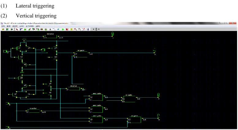
For latch up to occur, the parasitic npn- pnp circuit has to be triggered. Two distinct methods of triggering are possible:-
(1) Lateral triggering (2) Vertical triggering
Lateral triggering occurs when a current flows in the emitter of the lateral npn- transistor. The static trigger point is set by
Fig. 1 Circuit design of BCD to Excess-3 code converter
Fig. 2 Timing diagram
pnp on ntrigger
npn well
V
I
R
V
pnp on = 0.7V
npn= common base gain
R
well= well resistanceFrom above, we can see that if
R
well resistance increases triggering current becomes small and at the small value ofntrigger
I
, parasitic transistor is triggered. To examine the effect of this fault, we take the value ofR
well 100
. Vertical triggering occurs when a sufficient current is injected into the emitter of the vertical pnp- transistor.Latch up depends on the pulse widths, speed of the transistor. For latch up condition
npn+
pnp=1Where,
npn= cnen
I
I
,
pnp=cp
EP
I
I
3.2 Distributed RC effects
The propagation of a signal along a wire depends on many factors, including the distributed resistance and capacitance of the wire, the impedance of the driving source and the load impedance [7].
[image:2.595.53.442.105.318.2]A long wire can be represented in terms of several RC sections. The response at node Vj with respect to time is then
given by
j
dV
C
dt
= ( Ij-1 – Ij )=
(
V
j 1V
j)
(
V
jV
j 1)
R
R
If the number of sections in the network becomes large, the above expression reduces to the differential form:
2
2
dV
d V
rc
dt
dx
Where x= distance from input r= resistance per unit length c= capacitance per unit length
a discrete analysis of the circuit shown in figure gives an approximate signal delay of
0.7
(
1)
2
n
RCn n
t
Where n= number of sections
As n becomes very large, this reduces to
2
1
0.7
2
rcl
t
Where r= resistance per unit length c= capacitance per unit length l= length of the wire
The
2
l
term in equation shows that signal delay will betotally dominated by this RC effect for very long signal paths. To examine this effect, we take the value of R is 50
and C is 0.05 pf.3.3 Input waveform slope
If any circuit consists of many inputs, then different slope of the input waveforms can modify the delay of a gate. When the input rises or falls rapidly, the delay of the charge or discharge path is determined by the rate at which the transistors in the path can charge or discharge the capacitors in the tree. When the input changes slowly, it will contribute to the output delay. The rise time is given by
1 2
6
input fall dr dr step
t
t
t
p
Where
dr step
t
= the step-input rise time calculated in equationinput fall
t
= the input fall timetp DD
V
p
V
dr step p L
p
C
t
A
pA
= process constant for a specific supply voltage.
0 02(1
)
1
2
ln
1
1
p DDp
V
p
A
V
p
p
V
Similarly,
1 2
6
input rise df df step
t
t
t
n
tn DD
V
n
V
This is valid for input rise or fall times that satisfy the following criteria:
36
1
input rise p DD
L
t
V
p
C
p
and
36
1
input fall n DD
L
t
V
n
C
n
Three factors on which delay time depends:
(1)
t
d is directly proportional to load capacitance (C
L). (2)t
d is inversely proportional to supply voltage (V
DD).(3)
t
d is inversely proportional to
.To examine this fault we give the different time to the all input signals like low time (
t
l) 0.775 ns for input ‘d’, 1.540ns for input ‘c’, 2.975 ns for input ‘b’ and 7.975 ns for input ‘a’ .
m
3.4 Bridging fault
With the increase in the number or devices on the VLSI chips, the probability of shorts between two or more signal lines has been significantly increased. Unintended shorts between the lines form a class of permanent faults, known as bridging faults [8]. It has been observed that physical defects in MOS (Metal oxide semiconductor) circuits are created as bridging faults more than as any other type of fault. Bridging faults can be categorized into three groups:
Input bridging Feedback bridging Non feedback bridging
The probable bridging fault in the circuit (or in any other CMOS circuit) can be grouped into four categories.
Metal poly silicon short
To examine the effect of this fault, we take metal poly silicon shorting. Here four layout designs are shown below.
Fig. 3 Layout design of latch up fault
Fig.5 Layout design of input waveform slope
Fig.6 Layout design of bridging fault
4. EXPERIMENT RESULTS
Cmos
foundry
Without
fault(mW)
Latch up
fault (mW)
RC-effect
(mW)
Input waveform
slope (mW)
Bridging
fault (mW)
0.12
m
0.767 0.801 0.932 0.766 1.1050.18
m
0.418 0.424 0.738 0.412 0.8010.25
m
0.924 0.877 1.011 0.924 1.1755. CONCLUSION
Here we see that the various faults influence the different foundry in a different manner.
We saw the effect of faults that are following: (a) Latch up
(b) Distributed RC effect
(c) Delay fault on the input waveform (d) Bridging fault
Power consumption plays widespread role on any level design. In order to proper operation of any circuit, it requires that it gives desired output at the low power consumption. But during the process, many faults occur which are responsible to enhance the power consumption.
So, if we use optimization of the parameters, we can control the power consumption.
REFERENCES
[1] Angelika Janning, Johann Heyszl, Frederic Stumpf and Georg Sigl, September 28, 2011, ISBN 978-1-4577-1463-4. A cost –Effective FPGA-based Fault Simulation Environment.
[2] Mahmoud Shahbazi, Philippe Poure, Shahrokh Saadate and Mohammad Reza Zolghadri, September 6, 2011, ISSN 0278-0046. Fault Tolerant Five Leg Converter Topology with FPGA-based Reconfigurable Control. [3] Bogdan Alecsa, Marcian N. Cirstea and Alexandru Onea,
IEEE transactions on industrial informatics, vol.8, no.3, august 2012, ISSN 1551-3203.Simulink Modeling and Design of an efficient hardware-constrained FPGA-based PMSM speed controller.
[4] Todd Buerkle, Brock J. LaMeres, Todd Kaiser, Eric Gowens, Laurie Smoot, Tiffany Heetderks, Katie Schipf, Lizzy Clem, Steph Schielke and Rachael Luhr, IEEE sensors journal, vol.12, no.6,june 2012, ISSN 1530-437X. Ionizing Radiation Detector for Environmental Awareness in FPGA-based Flight Computers.
[5] Wen-Hui Chen & Chao-Tang Li, vol.35, issue 6, September 2012. Fault section estimation for distribution substations using on chip design.
[6] M. Morris Mano, Digital Logic and Computer Design, PHI.
[7] Neil and Waste, CMOS VLSI design circuits.
[8] Parag K. Lala, Fault tolerant and fault testable hardware design.
[9] Junfeng Fan, Xu Guo, Elke De Mulder and Patrick Schaumont, Hardware-Oriented
[10] Security and Trust (HOST), 2010 IEEE International Symposium on, 2010. State of the art of secure ECC implementations: a survey on known side- channel attacks and countermeasures.
[11] P. Duan, K. Xie, L. Zhang, and X. Rong. IEEE Transactions on Power Electronics, vol. 26, pp. 816-821, 2011. Open-switch fault diagnosis and system reconfiguration of doubly fed wind power converter used in a microgrid.
[12] D. Campos-Delgado and D. Espinoza-Trejo, IEEE Transactions on Industrial Electronics, vol. 58, pp. 671-679, 2011. An Observer-Based Diagnosis Scheme for Single and Simultaneous Open-Switch Faults in Induction Motor Drives
[13] S. Karimi, A. Gaillard, P. Poure, and S. Saadate, IEEE Transactions on Industrial Electronics, vol. 55, pp. 4299-4308, Dec 2008. FPGA-Based Real- Time Power Converter Failure Diagnosis for Wind Energy Conversion Systems.
[14] W. Sleszynski, J. Nieznanski, and A. Cichowski, IEEE Transactions on Industrial Electronics, vol. 56, pp. 4681-4688, 2009. Open-transistor fault diagnostics in voltage-source inverters by analyzing the load currents.
[15] D. U. Campos-Delgado, D. R. Espinoza-Trejo, and E. Palacios, IET Electric Power Applications, vol. 2, pp. 121-134, Mar 2008.,Fault tolerant control in variable speed drives: a survey.
[16] A. Yazdani, H. Sepahvand, M. L. Crow, and M. Ferdowsi, , IEEE Transactions on Industrial Electronics, vol. 58, pp. 1307-1315, 2011. Fault Detection and Mitigation in Multilevel Converter STATCOMs
[17] M. Turala, Nucl. Instrum. Methods Phys. Res., vol. 541, nos. 1–2, pp. 1–14, 2005.Silicon tracking detectors-historical overview,”