Threshold Voltage Control through Multiple Supply for
Low Power IG-FinFET Circuit
Manorama
Research Scholar ITM University
Pavan
Shrivastava
Research Scholar ITM University
Saurabh
Khandelwal
Research Scholar ITM University
Shyam Akashe
Associate Professor ITM University
ABSTRACT
As scale down the standard single-gate bulk MOSFET dimensions, vast challenges in the nanometer regime due to the brutal short-channel effects arises that grounds an exponential increases in the leakage current, power consumption and enriched the sensitivity in process variations. Double gate and multi-gate technology alleviate these restrictions by producing a stronger control over a thin silicon body with electrically coupled gates. In this paper, proposed a methodology for independent gate (IG) FinFET Nand circuit in which applies multiple supplies for controlling the threshold voltage by
which IG FinFET can improve the speed, saving the power and minimize the area of the circuit by 23-25%. The most advantageous IG keeper gate bias conditions are identified for reaching maximum savings (approx 40-43%) in delay and power (24-28%) while maintaining identical noise immunity as compared to the simple supply IG-FinFET domino circuits. Here the circuit efficiency also enhances.
Keywords
Independent gate FinFET circuit, High performance, Short channel effects (SCEs), Multiple supply, Threshold voltage, Cadence virtuoso tool.
1.
INTRODUCTION
As the technology scale down the channel length of the MOSFET from 10µm to 22nm above last 40 years. Gate-dielectric leakage currents and the enhanced circuit sensitivity to process parameter oscillation have become the leading barriers against further CMOS technology scaling into the sub-45nm regime. It is to facilitate the use of double gate metal oxide semiconductor field effect transistor (DGMOSFET), which produce better control of short channel effects, lower leakage current and enhanced scaling efficiency in the CMOS [1]. FinFET technology is the outstanding choice among Double gate MOSFET because it is quite easy and fashionable to manufacture and implementation rather than the other DGMOSFET. In the FinFET the use of lightly-doped channel makes it a resistant to random dopant variations [2].
t devices) is based on the “strong-inversion” provision at which the surface potential is twice of the bulk Fermi potential
.
(1)
Where VFB is the Flat band voltage and is the body factor. This
definition is not practical for measure since is not a calculable parameter. For this reason, consider here an explanation, based on a constant value at the turn-on condition, which is simple and
valid. Here, in the equation (2) show that high FinFET can
be obtained by carefully tuning the gate oxide thickness and electrode work function, and without the use of any extra bias voltage. The threshold voltage of FinFET is given by the expression:
(2) Here variation between work function of electrode and silicon is , is the depletion charge in the channel, and is the
gate capacitance. is a constant that represents the limited
availability of inversion charges in the undoped channel [4]. FinFET technology has an important characteristic that is dynamic controllability, in which the of one gate of a
FinFET can be switched through the function of a voltage at the other gate. Since the manages both transistor power
consumption and the speed of the circuit, controllability is
dominant factor for circuit optimization. Mainly in this paper apply the controllability technique on the Independent gate
(IG) mode FinFET, in this mode of FinFET the number of transistors mandatory for implementing specific logic functions are less as compared to the standard circuits with short gate FinFET. Area saving, condensed power consumption, considerable speed improvement is exhibited due to the reduced parasitic capacitance and the lesser transistor stack heights with the independent gate FinFET circuits as compared to the circuits with short gate[6], [7]. In this paper a new circuit synthesis style based on multiple supply and threshold voltages is presented, it is an innovative way to control of connected gate FinFET. In
conventional multiple supply voltages formats, logic gates on the critical path are usually allotted a high supply voltage although the gates on the non critical paths are connected to a low supply voltage in order to diminish power consumption as maintaining circuit performance. In accumulation to multiple supply voltage design technique, the low value of can sustain the high
Fig1. Cross sectional of a usual FinFET.
The paper is structured as follows. In Section II we would discuss, Independent Gate FinFET and its working. Section III discussed the principle for threshold voltage control by multiple supplies which forms the source for the scheme presented in this paper. Section IV presented the experimental results and conclusion in Section V.
2.
INDEPENDENT GATE FINFET
Designing of different FinFET circuit can be organized in one of the consequent modes, (a) Shorted gate or tied gate mode, in which both gates are tied together and get improved drive strength and have better control over the channel length (b) independent gate mode, in this mode independent signals drive both the gates, this may reduce the number of transistors in the circuit.(c) Low-power mode, in which applying a low voltage to n-type FinFET and high voltage to p-type FinFET. This varies the threshold voltage of the devices which reduces the leakage power dissipation at the cost of increased delay. (d) A hybrid IG/LP-mode is a combination of LP and IG modes [10]. Independent gate FinFET circuit can be fabricated along with the usual short gate FinFETs circuits on the unchanged die, by removing the top gate region of the FinFETs. The formation of channel in one gate is extremely dependent on the state of the other gate because of electrostatic pairing between the gates. If as an illustration that the back gate of an independent gate FinFET is disabled then no channel will form near the disabled gate due to electrostatic pairing between the gates and the of the other gate will be increased. Mainly in these devices, only one gate is turned on, the is high adequate to stop channel
formation. If both gates are turned on, fast electrostatic pairing between the gates decrease the and allow channel formation.
In addition, high Vth FinFET circuits can be activated only if both of their gates are turned on at the same time by this enhance the circuit performance and reduce the area of the circuit. The threshold voltage of an n-channel MOSFET is classically given by:
(3) Where ϕms is the work function variation between the gate and the silicon and called it as gate barrier. The Barrier measurement in the gate definition defines the work function difference between the metal and an intrinsic reference semiconductor. Relation between gate barrier and ϕms is given by following equations:
Above equations clearly specify the dependence of threshold voltage on gate barrier. For higher threshold voltage the value of barrier should be high. A broad range of threshold voltage can be achieved by varying gate barrier. The threshold voltage of device is found to be advanced for high barrier.
Fig.2 shows the waveform Threshold voltage ( ) versus channel length for the n channel FinFET.
In the Figure 2 versus channel length waveform for nmos
FinFET at the Cadence virtuoso tool at 45nm. In which the normal nmos FinFET transistor threshold voltage is 0.46v, it can be seen in figure2. Essentially, the of nmos openly depends
on work function difference between the gate and the channel. The difference between the gate and channel is called gate barrier, deviation in gate barrier has main effect in increasing the threshold voltage. Here, independent gate Nand FinFET for
variations. Figure 3 shows the schematic of IG mode Nand
FinFET in which minimize one pmos transistor.
Fig3. Schematic of Independent gate Nand FinFETs.
3.
THRESHOLD VOLTAGE CONTROL
BY MULTIPLE SUPPLY
The of the each FinFET gate can not only be controlled by
the process parameters, such as channel dopant concentration or the work function of the gate, but also enthusiastically through the application of a voltage to the other gate (gate-gate pairing). A comprehensive representation for the relation in between the
Vdd
Output
A
B
Front
Gate
Back Gate
Channel (undoped)
Source n+ Draintox
t
Siand V0thgf (minimum observed value of Vthgf) would be adequate
[14] has been shown in equation 4.
if ,
or else. (4)
Here, δ is a positive coefficient whose value depends on the ratio of gate and body capacitances. In the short gate mode of FinFET the threshold voltage of both gates react simultaneously to the change in the voltage of another gate. It occurs because the back gate is in depletion mode and charge pairing arises between the front gate and back gate. On the other hand, when the back gate is in strong inversion mode, the free charge carriers efficiently screen the back gate electric field, manufacturing Vthgf independent of Vgbs. For the delay calculation of the circuit in equation 5:
(5)
Here C is the load capacitance, Vdd is the supply voltage and Vth is the threshold voltages of the MOS transistors.
Fig4. Independent gate Nand FinFET using multiple supply at cadence virtuoso tool.
Independent gate Nand FinFET circuit is implemented with the help of one pmos and two nmos. Figure 4 shows that the Independent gate Nand FinFET with another voltage supply to the substrate and the back gate by this implementation by this control the of whole circuit.
4.
SIMULATION AND RESULT
In this section Firstly, present a comparative analysis of simple IG-FinFET Nand i.e. two input supply and the main supply (VDD) and the multiple supply based IG-FinFET Nand at 45nm
Cadence Virtuoso tool. Figure 5 and 6 shows the output response of the simple IG-FinFET Nand and multiple supplies IG-FinFET Nand. As the output response waveform shows the drawback of the implementation, here the leakage current of the circuit increases by approximately 18-23%.
Fig5. Simulation Waveform of simple IG-FinFETs Nand two inputs, output and the leakage current.
[image:3.595.291.511.252.394.2]F Fig6. Simulation Waveform of multiple supplies IG-FinFETs Nand
Figure 6 shows the waveform of multiple supplies IG-FinFET Nand two inputs, output and the leakage current.
Mainly, these simulation waveforms indicate the behavior performance of the schematic. The regarding schematic is
shown in figure 4.
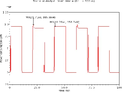
Fig8. Shows the power consumption waveform of the multiple supply IG-FinFET Nand.
For the power consumption observes the figure 7 and 8. By using multiple supplies IG-FinFET Nand circuit consume 30-40% less power than the simple IG-FinFET. In the case of threshold control by the multiple supply, then such type of results that are, if consider two supplies to IG-FinFET Nand than nmos is 0.65v or for pmos is -0.58v and if consider
multiple supply IG-FinFET Nand than nmos is 0.53v or for
pmos is -0.44v. Because of this threshold voltage variation such results which are shown in the table 1. These simulation results have been performed on Cadence Virtuoso Tool.
Table 1. Shows the comparison results in between the two implementation technique on IG-FinFET Nand.
Performance parameters
Simple Supply IG-FinFET Nand
Nmos Vth= 0.65v
Pmos Vth= -0.58v
Multiple Supply IG-FinFET Nand
Nmos Vth= 0.53v
Pmos Vth= -0.44v
Delay 160.9 ps 67.51 ps
Duty Cycle 77.82% 82.34%
Power Consumption
4.83 nw 1.25 nw
5.
CONCLUSION
IG-FinFET offers a calculated way for variable threshold voltage. It is also possible in IG-FinFET to fluctuate the threshold voltage during the operation by connecting the additional supplies receive a good range of threshold voltages. Single IG-FinFET can also be used as two coupled transistor therefore with IG- mode of operation have a broad range of threshold voltage as well as considerable area efficiency. But there are some negative aspects while using FinFET in IG mode like the high sub-threshold leakage. This paper mainly focused on the threshold control by multiple supply voltage. As in figure 4 offers the additional supply on the back gate and this enhances
7-10% of the circuit. The total power consumption of the circuit also varies from 24-28% using this implementation.
6.
ACKNOWLEDGMENT
This work is supported by ITM University, Gwalior, India in Collaboration with Cadence System Design, Bangalore, India
7.
REFERENCES
[1] Sherif A. Tawfik and Volkan Kursun, “Low-Power and Compact Sequential Circuits With Independent-Gate FinFETs”, JANUARY 2008,IEEE TRANSACTIONS ON ELECTRON DEVICES, VOL. 55, NO. 1.
[2] Anish Muttreja, Prateek Mishra and Niraj K. Jha, “Threshold Voltage Control through Multiple Supply Voltages for Power-efficient FinFET Interconnects”, 2008, 21st International Conference on VLSI Design, IEEE. [3] B. Swahn and S. Hassoun. Gate sizing: FinFETs vs 32nm
bulk MOSFETs. July 2006, In Proc. Design Automation Conf., pages 528–531.
[4] J. Colinge, FinFETs and other multi-gate transistors. Springer, Nov. 2007.
[5] D. Hisamoto, L. Wen-Chin, J. Kedzierski, H. Takeuchi, K. Asano, C. Kuo, E. Anderson, K. Tsu-Jae, J. Bokor, and H. Chenming, (2000) "FinFET – a self-aligned double-gate MOSFET scalable to 20 nm," IEEE Trans. Electron Devices, vol. 47, pp. 2320-2325.
[6] Masoud Rostami and Kartik Mohanram “Novel dual-Vth independent-gate FinFET circuits” 2010, Digital Object Identifier: 10.1109/ASPDAC.2010.5419680, Page(s): 867 – 872.
[7] Muttreja, N. Agarwal, and N. K. Jha, “CMOS logic design with independent gate FinFETs,” 2007, in Proc. Int. Conf. Computer Design, Oct., pp. 560–567.
[8] K. Usami, M. Igarashi, F. Minami, T. Ishikawa, M. Kanzawa, M. Ichida, and K. Nogami, “Automated low-power technique exploiting multiple supply voltages applied to a media processor,” Mar. 1998, IEEE J. Solid-State Circuits, vol. 33, no. 3, pp. 463–472.
[9] K. Roy, L. Wei, and Z. Chen, “Multiple-Vdd and multiple-Vth CMOS (MVCMOS) for low-power applications,” in Proc. Int. Symp. Computer Architecture, Oct. 1999, pp. 366–370.
[10]V Narendar, Wanjul Dattatray R, Sanjeev Rai and R. A. Mishra, “Design of High-performance Digital Logic Circuits based on FinFET Technology”, March 2012, International Journal of Computer Applications (0975 – 8887) Volume 41– No.20,.
[11]M.H. Chiang, Keunwoo Kim, Ching-Te Chaung and Tretz C, “High-density reduced-stack logic circuit techniques using independent-gate controlled double-gate devices”, Sep. 2006 IEEE Trans. Electron Devices, vol. 53, no. 9, pp. 2370–2377.
[image:4.595.58.269.75.234.2][14]A. Muttreja, P. Mishra, and N. K. Jha, “Threshold voltage control through multiple supply voltages for power-efficient FinFET interconnects,” Jan. 2008, in Proc. Int. Conf. VLSI Design.
[15]V.Raj Kumar and A. Alfred kirubaraj, “Submicron 70nm CMOS Logic Design With FINFETs”, International Journal of Engineering Science and Technology Vol. 2(9), 2010, 4751-4758.
[16]S. A. Tawfik, V. Kursun, Asymmetric dual-gate multi-fin keeper bias options and optimization for low power and robust FinFET domino logic, in Proceedings of the IEEE Asia Pacific Conference on Circuits and Systems, December 2008, pp. 1720–1723.
[17]S. A. Tawfik, V. Kursun, High speed FinFET domino logic circuits with independent gate-biased double-gate keepers providing dynamically adjusted immunity to noise, in: Proceedings of the IEEE International Conference on Microelectronics, December 2007, pp.175–178.
[18]D. Fried, J.S. Duster and K.T. Kornegay, “Improved Independent Gate N-Type FinFET Fabrication and
Characterization,” in IEEE Electron Device Letter, Vol. 24, No. 9, September 2003, pp. 593.
[19]S. O'uchi, K. Sakamoto, K. Endo, M. Masahara, T. Matsukawa, Y.X. Liu, M. Hioki, T. Nakagawa, T. Sekigawa, H. Koike and E. Suzuki, “Variable-Threshold-Voltage FinFETs with a Control-“Variable-Threshold-Voltage Range with in the Logic-Level Swing Using Asymmetric Work-Function Double Gates,” 2008 in VLSI Technology, Systems and Applications,.
[20]D. M. Fried, E. J. Nowak, J. Kedzierski, J. S. Duster,and K. T. Kornegay. A fin-type independent double-gate NFET June 2003 In Proc. Device Research Conf., pages 45–46. [21]H. Mahmoodi, S. Mukhopadhyay, and K. Roy. High
performance and low power domino logic using independent gate control in double-gate SOI MOSFETs. Oct. 2004 In Proc. IEEE Int. SOI Conf., pages 67–68. [22]W. Zhang, J. G. Fossum, L. Mathew, and Y. Du. Physical
insights regarding design and performance of independent-gate FinFETs. Oct. 2005 IEEE Electronic Device Lett., 52(10):2189–2206.