N A N O E X P R E S S
Open Access
Facile Preparation of a Platinum Silicide
Nanoparticle-Modified Tip Apex for
Scanning Kelvin Probe Microscopy
Chun-Ting Lin
1, Yu-Wei Chen
2, James Su
1, Chien-Ting Wu
3, Chien-Nan Hsiao
1, Ming-Hua Shiao
1*and Mao-Nan Chang
2,4*Abstract
In this study, we propose an ultra-facile approach to prepare a platinum silicide nanoparticle-modified tip apex (PSM tip) used for scanning Kelvin probe microscopy (SKPM). We combined a localized fluoride-assisted galvanic replacement reaction (LFAGRR) and atmospheric microwave annealing (AMA) to deposit a single platinum silicide nanoparticle with a diameter of 32 nm on the apex of a bare silicon tip of atomic force microscopy (AFM). The total process was completed in an ambient environment in less than 3 min. The improved potential resolution in the SKPM measurement was verified. Moreover, the resolution of the topography is comparable to that of a bare silicon tip. In addition, the negative charges found on the PSM tips suggest the possibility of exploring the use of current PSM tips to sense electric fields more precisely. The ultra-fast and cost-effective preparation of the PSM tips provides a new direction for the preparation of functional tips for scanning probe microscopy.
Background
With the prosperous development of nanotechnology, the demand on nondestructive analysis of the distri-bution of charge density [1], magnetic field [2], sur-face potential [3], etc. is surging in nanometrology. In the field of nondestructive analysis, scanning Kelvin probe microscopy (SKPM) has been widely used to analyze the surface potential distribution of materials [4–6]. Spatial resolutions of the geometry and surface potential are both crucial issues in SKPM. Tradition-ally, apexes of silicon (Si) tips coated with metallic thin film, e.g., platinum-iridium alloy (PtIr), are widely used for SKPM. However, the spatial resolution was seriously limited because of the stray-field generated by the metallic coating [7–9]. To reduce this stray-field phenomenon, many nanostructures have been proposed for tip modifications, including carbon nanotube [10–12], Pt nanowire [13], single metallic nanoparticle (NP) [14, 15], etc. Moreover, for many
decades, electron beam induced deposition (EBID) has been a major approach for tip modification [16–19]. However, the vacuum system required for the EBID process and the need to manipulate electron beams make the tip modification costly and inefficient. For these reasons, the development of nonvacuum tech-nology for tip modifications has been presented. Elec-trodeposition [15] and electroless deposition [14] are both feasible approaches for tip modification under ambient conditions. Recently, we successfully prepared an apex of an Ag NP-modified silicon tip (Ag tip) by utilizing a localized fluoride-assisted galvanic replace-ment reaction (LFAGRR), which provides a facile and cost-effective process for tip modification [14]. However, the instability of Ag under ambient conditions directly limits the commercialization of the Ag tips [20]. In this paper, the LFAGRR was extended to prepare Pt NP-modified silicon tip apexes (Pt tips). Moreover, we introduced atmospheric microwave annealing (AMA) to further stabilize the tip apexes by transforming the Pt tips into platinum silicide NP-modified tip apexes (PSM tips). Scanning electron microscopy (SEM), transmission electron microscopy (TEM), SKPM, and * Correspondence:mhshiao@narlabs.org.tw;mnchang@dragon.nchu.edu.tw
1
Instrument Technology Research Center, National Applied Research Laboratories, Hsinchu 300, Taiwan
2
Department of Physics, National Chung Hsing University, Taichung 402, Taiwan
Full list of author information is available at the end of the article
electrostatic force microscopy (EFM) were employed to study the PSM tips and the corresponding Si-based Pt silicide NPs. Our results demonstrate that the PSM tips benefit from both high spatial resolutions of topog-raphy and surface potential. Moreover, the facile and cost-effective approach combining the LFAGRR and AMA provides a new direction for preparing functional tips for scanning probe microscopy.
Methods
Preparation of Pt and PSM Tips
Figure 1 shows the schema of the fabrication process of the PSM tips. In a typical LFAGRR process, we utilized a slice of commercial anodic aluminum oxide (AAO) with 100 nm of pore size (Whatman) as the template for carrying the electrolyte comprising 0.01 M chloro-platinic acid (H2PtCl6) and 16 % (v/v) buffered oxide etchant (BOE) (comprising 34 % NH4F and 7 % HF). The prepared AAO template was followed by a con-tinuous tapping process for 30 s in the atomic force mi-croscopy (AFM) (Bruker D3100) by utilizing silicon tips (NANOSENSORS) to form Pt NP on the tip apexes, de-noted as Pt tips. The prepared tips then underwent the AMA process in a commercial microwave oven (Freser MW-1806) at 1800 W for 60 and 90 s, respectively. The prepared tip apexes were denoted as PSM-60 and PSM-90 tip. We also employed an n-type Si wafer that was dipped in the same electrolyte for various durations and had undergone the same AMA for SEM and TEM analysis.
Surface Morphology and Material Characterization SEM (Hitachi S-4000) and TEM (JEOL JEM2010F) were employed to investigate the surface profile of the prepared samples. Energy-dispersive X-ray spectroscopy (EDS) was used to analyze the elemental composition. The SKPM and EFM images were acquired by a scanning probe microscope (Bruker D3100). The SKPM measurement pa-rameters were image size = 2μm, scanning rate = 0.2 Hz, lift height = 30 nm, Vac= (1.1–1.5) V, and ω2= (31–35)
kHz. The EFM measurement parameters were: image size = 1 μm, scanning rate = 0.5 Hz, lift height = 30 nm, and substrate bias = (0,−0.5,−1.0,−1.5) V, respectively. All measurements were performed in constant environment conditions with temperature = (20 ± 0.3) °C and relative humidity = (40 ± 5) % RH. All of the chemicals used in the experiment were reagent grade.
Results and Discussion
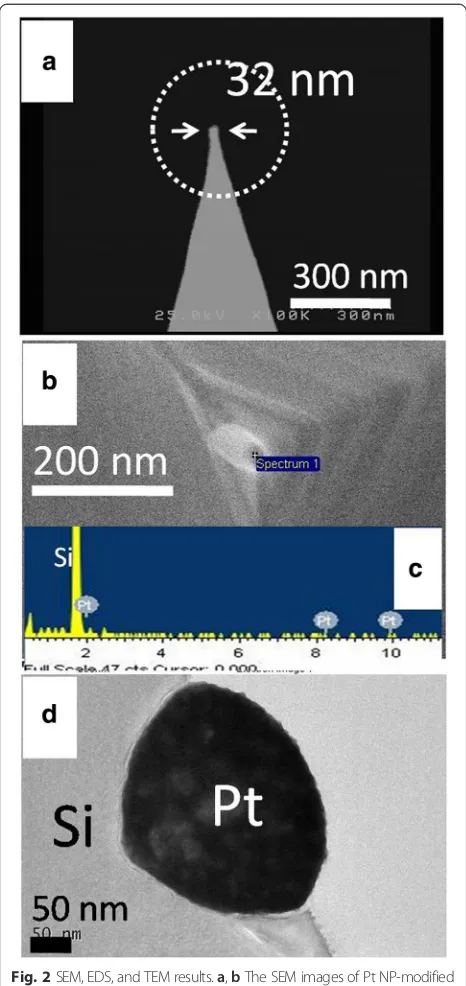
Figure 2a, b shows the typical Pt tip prepared by the LFAGRR before conducting the AMA process. A Pt NP with a 32 nm diameter can be clearly observed, which coincides with our previous report about Ag tips [14]. The ingredient of the Pt tip was verified using EDS (Fig. 2c). Figure 2d shows the TEM image of Pt NP-modified Si base prepared by the fluoride-assisted gal-vanic replacement reaction (FAGRR). The pinecone-like Pt NPs were found embedded into the Si domain, which agrees with the previous Pt nanostructures reported by Ye et al. [21]. We also noted that the Pt NPs elongated and embedded more into the Si domain as the duration of the reaction increased (Fig. 3).
Figure 4 shows the SEM images of typical PSM tips (Fig. 4a, b) and the TEM images of the corresponding Pt NP-modified Si wafer obtained after it was exposed to various AMA conditions (Fig. 4c, e). The morphology of the tip apexes was unchanged compared to that before exposure to AMA conditions (Fig. 2a). However, an ob-vious interface diffusion was observed between Pt and Si in the TEM images (Fig. 4c, e). Moreover, the formation of Pt3Si was verified by the selected area diffraction (SAD) in the TEM (Fig. 4d, f ). Note that microwave an-nealing is a common process in the semiconductor field [22, 23]. However, few previous studies report the formation of Pt silicide using microwave annealing. Thermal annealing is commonly used in the preparation of Pt silicide-modified AFM tips [24, 25]. Besides, Chou et al. reported the formation of platinum silicide by annealing the junction between silicon carbide and Pt
[image:2.595.60.541.576.723.2][26]. Takahashi et al. utilized silane to react with Pt at 250 to 400 °C to form platinum silicide [27]. Wang et al. prepared Pt silicide by thermal annealing of a Pt/SiO2 junction in a hydrogen environment [28]. A similar form of hydrogen annealing has also been
adopted by Liu et al. to prepare Pt3Si for benzene oxidation [29]. Compared to these efforts on thermal annealing, our AMA process provides a facile and cost-effective process for the preparation of Pt silicide.
Figure 5 shows the SKPM images of Si-based Ag NPs acquired using a bare silicon tip (Fig. 5a1, a2), a commercial PtIr-coated silicon tip (Fig. 5b1, b2), a PSM-60 tip (Fig. 5c1, c2), and a PSM-90 tip (Fig. 5d1, d2), respectively. Figure 5a3, b3, c3, d3 are the SEM images of the corresponding tips used in the SKPM measurements. The SKPM images obtained using PSM tips demonstrate clear potential contrast compared to that obtained by either commercial PtIr-coated Si or bare Si tips. Moreover, the resolution of topography of AFM images acquired using PSM tips stayed nearly the same as that of images acquired using a bare Si tip. The results in Fig. 5 revealed that PSM tips are capable of enhancing the spatial resolution of surface potentials while maintaining the resolution of topog-raphy. It is noted that the commercial PtIr-coated Si tips require vacuum based processes, e.g., sputter or e-beam assisted deposition. So that the PtIr-coated Si tips suffer from high cost and the sacrifice of sharp-ness at the tip apexes. In contrast, our PSM tips can be fabricated under ambient conditions in less than 3 min by combining LFAGRR and AMA. The local-ized electroless deposition maintains the sharpness of the tip apexes. Also, the vacuum-free fabrication promin-ently reduces the cost of the PSM tips. In addition, the negative shift of the surface potential found on the SKPM profiles collected using PSM tips suggests that the work function of the tip apexes varied with the AMA process, which could be attributed to the for-mation of Pt3Si that varies the work function of the tip apex.
Besides the enhanced spatial resolution of the surface potential, the PSM tip was negatively charged. Figure 6 shows the EFM images of Si-based Au nanoislands under various biases. No phase difference was found when zero bias was applied to the Au nanoislands. When the substrate of the Au nanoislands was sub-jected to a more negative bias, the phase difference became clearer, which means that the repulsive force between the PSM tip and the Au islands became stron-ger. That phenomenon provided direct evidence that the PSM tip was negatively charged. The result could be attributed to the formation of Pt silicide that reduces the Schottky barrier and enables the electron injection from the domain of n-type Si to platinum [24, 30, 31]. Our results demonstrated the possibility of engineering tip apexes with confined charges for more precise sens-ing of electrical fields. In addition, the ultra-fast and cost-effective preparation of PSM tips provides a new Fig. 2SEM, EDS, and TEM results.a,bThe SEM images of Pt NP-modified
silicon tip apex.c The corresponding EDS analysis ofb.dThe TEM image of Pt NPs grown on planar Si using fluoride-assisted galvanic replacement reaction. The electrolyte for Pt deposition is composed of 0.01 M of H2PtCl6and 16 % (v/v) buffered oxide
[image:3.595.57.290.88.581.2]direction for preparing functional tips for scanning probe microscopy.
Conclusions
In summary, we proposed an ultra-facile process com-bining LFAGRR and AMA to prepare PSM tips under ambient conditions. The improved potential resolution of Si-based Ag nanoislands in SKPM measurement was
realized. Moreover, the resolution of the topography was comparable to that of a bare silicon tip. In addition, the negative charges found on the PSM tips suggests the possibility of exploring the use of current PSM tips to sense electric fields more precisely. The ultra-fast and cost-effective preparation of the PSM tips provides a new direction for preparing functional tips for scanning probe microscopy.
Fig. 3The SEM images of Pt NP-modified planar silicon prepared by FAGRR for various reaction durations. The electrolyte for Pt deposition is composed of 0.01 M of H2PtCl6and 16 % (v/v) buffered oxide etchant (BOE)
[image:4.595.59.539.88.310.2] [image:4.595.58.539.486.695.2]Fig. 5The SKPM images of Si-based Ag nanoislands and the SEM images of the corresponding tips used in the measurement. The SKPM images of Si-based Ag nanoislands acquired by using a bare Si tip (a1,a2), PtIr-coated Si tip (b1,b2), PSM-60 tip (c1,c2), and PSM-90 tip (d1,d2). The SEM images for the bare Si tip (a3), PtIr-coated Si tip (b3), PSM-60 tip (c3), and PSM-90 tip (d3)
Fig. 6The EFM images of Si-based Au nanoislands acquired by using a PSM-60 tip for various applied biases on the substrate. The applied bias was 0 V forb,−0.5 V ford,−1.0 V forf, and−1.5 V forh.a,c,e,gThe corresponding topographies acquired by applying AFM tob,d,
[image:5.595.57.541.89.433.2] [image:5.595.53.540.469.697.2]Competing interests
The authors declare that they have no competing interests.
Authors’contributions
CT, MH, and MN prepared the manuscript jointly. MH and MN are the principal investigators of this research project. YW contributed to the preparation of experimental samples and the SKPM measurement. JS contributed to the EFM measurement. CT contributed to the TEM investigation. CN participated in the major discussion and contributed to the interpretation of the surface analytical results. All authors read and approved the final manuscript.
Acknowledgments
The authors would like to express appreciation to the Ministry of Science and Technology (MOST) of the Republic of China, Taiwan, for the financial supports under the following contract numbers: MOST104-2221-E-492-001, MOST104-2623-E-492-001-ET, and NSC101-2112-M-492-002-MY3.
Author details
1Instrument Technology Research Center, National Applied Research
Laboratories, Hsinchu 300, Taiwan.2Department of Physics, National Chung Hsing University, Taichung 402, Taiwan.3National Nano Device Laboratories,
National Applied Research Laboratories, Hsinchu 300, Taiwan.4Institute of Nanoscience, National Chung Hsing University, Taichung 402, Taiwan.
Received: 24 August 2015 Accepted: 27 September 2015
References
1. Hong J, Noh K, Park S-i, Kwun S, Khim Z (1998) Surface charge density and evolution of domain structure in triglycine sulfate determined by electrostatic-force microscopy. Phys Rev B 58(8):5078
2. Häberle T, Schmid-Lorch D, Karrai K, Reinhard F, Wrachtrup J (2013) High-dynamic-range imaging of nanoscale magnetic fields using optimal control of a single qubit. Phys Rev Lett 111(17):170801 3. Hallam T, Lee M, Zhao N, Nandhakumar I, Kemerink M, Heeney M et al
(2009) Local charge trapping in conjugated polymers resolved by scanning Kelvin probe microscopy. Phys Rev Lett 103(25):256803
4. Nichols JA, Gundlach DJ, Jackson TN (2003) Potential imaging of pentacene organic thin-film transistors. Appl Phys Lett 83(12):2366–2368
5. Evers S, Senöz C, Rohwerder M (2013) Spatially resolved high sensitive measurement of hydrogen permeation by scanning Kelvin probe microscopy. Electrochim Acta 110:534–538
6. Hu Y, Berdunov N, Di CA, Nandhakumar I, Zhang F, Gao X et al (2014) Effect of molecular asymmetry on the charge transport physics of high mobility n-type molecular semiconductors investigated by scanning Kelvin probe microscopy. ACS Nano 8(7):6778–6787
7. Nonnenmacher M, O’Boyle MP, Wickramasinghe HK (1991) Kelvin probe force microscopy. Appl Phys Lett 58(25):2921–2923
8. Sacha GM, Verdaguer A, Martinez J, Saenz JJ, Ogletree DF, Salmeron M (2005) Effective tip radius in electrostatic force microscopy. Appl Phys Lett 86(12):123101–123103
9. Folks L, Best ME, Rice PM, Terris BD, Weller D, Chapman JN (2000) Perforated tips for high-resolution in-plane magnetic force microscopy. Appl Phys Lett 76(7):909–911
10. Minhua Z, Vaneet S, Haoyan W, Robert RB, Jeffrey AS, Fotios P et al (2008) Ultrasharp and high aspect ratio carbon nanotube atomic force microscopy probes for enhanced surface potential imaging. Nanotechnology 19(23):235704
11. Nguyen CV, Chao K-J, Stevens RM, Delzeit L, Cassell A, Han J et al (2001) Carbon nanotube tip probes: stability and lateral resolution in scanning probe microscopy and application to surface science in semiconductors. Nanotechnology 12(3):363
12. Hafner JH, Cheung C-L, Oosterkamp TH, Lieber CM (2001) High-yield assembly of individual single-walled carbon nanotube tips for scanning probe microscopies. J Phys Chem B 105(4):743–746
13. Chen PL, Su J, Shiao MH, Chang MN, Lee CH, Liu CW. Scanning electron beam induced deposition for conductive tip modification. Nano/Micro Engineered and Molecular Systems (NEMS), 2012 7th IEEE International Conference on; 2012 5–8 March 2012. doi:10.1109/NEMS.2012.6196836
14. Lin C-T, Yu M-H, Su J, Chen P-L, Shiao M-H, Nemcsics A et al (2013) Localized electroless Ag plating at a tip apex for scanning Kelvin probe microscopy. Jpn J Appl Phys 52(6):06GF3–GF3-4
15. Lin H-M, Chang M-N, Lin Y-S, Cheng C-C (2010) The manufacturing of a metallic nano-cluster at a tip apex for field-sensitive microscopy applications. J Nanosci Nanotechnol 10(7):4459–4464
16. Brown J, Kocher P, Ramanujan CS, Sharp DN, Torimitsu K, Ryan JF (2013) Electrically conducting, ultra-sharp, high aspect-ratio probes for AFM fabricated by electron-beam-induced deposition of platinum. Ultramicroscopy 133:62–66
17. Chen I-C, Chen L-H, Orme C, Quist A, Lal R, Jin S (2006) Fabrication of high-aspect-ratio carbon nanocone probes by electron beam induced deposition patterning. Nanotechnology 17(17):4322
18. Schiffmann KI (1993) Investigation of fabrication parameters for the electron-beam-induced deposition of contamination tips used in atomic force microscopy. Nanotechnology 4(3):163
19. Utke I, Hoffmann P, Berger R, Scandella L (2002) High-resolution magnetic Co supertips grown by a focused electron beam. Appl Phys Lett 80(25):4792–4794
20. Elechiguerra JL, Larios-Lopez L, Liu C, Garcia-Gutierrez D, Camacho-Bragado A, Yacaman MJ (2005) Corrosion at the nanoscale: the case of silver nanowires and nanoparticles. Chem Mater 17(24):6042–6052 21. Ye W, Liu J, Liu Q, Zhou F, Liu W (2010) Surfactant-free and controllable
synthesis of hierarchical platinum nanostructures and their comparative studies in electrocatalysis, surface-enhanced Raman scattering and surface wettability. Electrochim Acta 55(28):8649–8654
22. Bykov YV, Eremeev AG, Zharova NA, Plotnikov IV, Rybakov KI, Drozdov MN et al (2003) Diffusion processes in semiconductor structures during microwave annealing. Radiophys Quantum El 46(8–9):749–755 23. Yao-Jen L, Bo-An T, Chiung-Hui L, Zheng-Yao C, Fu-Kuo H, Po-Jung S et al
(2013) Low-temperature microwave annealing for MOSFETs with high-k/metal gate stacks. IEEE Electron Device Lett 34(10):1286–1288
24. Bhaskaran H, Sebastian A, Despont M (2009) Nanoscale PtSi tips for conducting probe technologies. IEEE Trans Nanotechnol 8(1):128–131 25. Bhushan B, Palacio M, Kwak KJ (2008) Thermally-treated Pt-coated silicon
AFM tips for wear resistance in ferroelectric data storage. Acta Mater 56(16):4233–4241
26. Chou TC (1991) High temperature reactions between SiC and platinum. J Mater Sci 26(5):1412–1420
27. Takahashi Y, Ishii H, Murota J (1985) New platinum silicide formation method using reaction between platinum and silane. J Appl Phys 58(8):3190–3194
28. Wang D, Penner S, Su DS, Rupprechter G, Hayek K, Schlögl R (2003) Silicide formation on a Pt/SiO2 model catalyst studied by TEM, EELS, and EDXS. J Catal 219(2):434–441
29. Liu G, Yang K, Li J, Tang W, Xu J, Liu H et al (2014) Surface diffusion of Pt clusters in/on SiO2 matrix at elevated temperatures and their improved catalytic activities in benzene oxidation. J Phys Chem C 118(39):22719–22729 30. Murarka SP (1983) Silicides for VLSI applications. Academic Press; San Diego.
ISBN:978-0-12-511220-8. doi:10.1016/B978-0-08-057056-3.50001-X 31. Murarka S, Kinsbron E, Fraser D, Andrews J, Lloyd E (1983) High temperature
stability of PtSi formed by reaction of metal with silicon or by cosputtering. J Appl Phys 54(12):6943–6951
Submit your manuscript to a
journal and benefi t from:
7 Convenient online submission
7 Rigorous peer review
7 Immediate publication on acceptance
7 Open access: articles freely available online
7 High visibility within the fi eld
7 Retaining the copyright to your article