N A N O E X P R E S S
Open Access
Galvanic synthesis of three-dimensional and
hollow metallic nanostructures
Sun Hwa Park
1,5, Jin Gyeong Son
2, Tae Geol Lee
1, Jongwon Kim
3, Sang Yun Han
4, Hyun Min Park
1,5and Jae Yong Song
1,5*Abstract
We report a low-cost, facile, and template-free electrochemical method of synthesizing three-dimensional (3D) hollow metallic nanostructures. The 3D nanoporous gold (3D-NPG) nanostructures were synthesized by a galvanic replacement reaction (GRR) using the different reduction potentials of silver and gold; hemispherical silver nanoislands were electrochemically deposited on cathodic substrates by a reverse-pulse potentiodynamic method without templates and then nanoporous gold layer replicated the shape of silver islands during the GRR process in an ultra-dilute electrolyte of gold(III) chloride trihydrate. Finally, the wet etching process of remaining silver resulted in the formation of 3D-NPG. During the GRR process, the application of bias voltage to the cathode decreased the porosity of 3D-NPG in the voltage range of 0.2 to−0.62 V. And the GRR process of silver nanoislands was also applicable to fabrication of the 3D hollow nanostructures of platinum and palladium. The 3D-NPG nanostructures were found to effectively enhance the SERS sensitivity of rhodamine 6G (R6G) molecules with a concentration up to 10−8M.
Keywords:Nanoporous; Gold; Platinum; Palladium; Galvanic reaction
Background
Nanoporous gold (NPG) structures have received a great deal of attention due to their potential applications in the fields of double layer capacitors, fuel cells, biosen-sors, electrocatalysis, etc. [1-4]. Many researchers have studied nanoporous metallic materials with a large spe-cific surface area (i.e., narrow pore-size distributions), because the nanoporosity affects not only active sites and electron mobility in the solid ligaments but also geometrical confinement effects [4-8]. It was reported that Pt-coated NPG nanostructures with smaller pore-size exhibited a higher catalytic activity in methanol oxi-dation than those with larger pore-size [9-11]. Recently, it was demonstrated that the surface enhanced Raman spectroscopy (SERS) effects of NPG depended on the pore size, the ratios of ligaments to nanopores, and the surface roughness [12,13].
The typical methods of synthesizing NPG structures have been electrodeposition, anodization, and dealloying processes [14-16]. Generally, three-dimensional (3D) structures of NPG have been fabricated using the hard or soft templates of porous membranes and self-assembled spheres of dielectric/conductive materials [9-11,17-20]. Recently, dual-templates of porous alumina and polystyrene microspheres were utilized to fabricate hierarchical macro/mesoporous gold wires [21]. Due to the combination of high specific surface area and easy transport of reactants in an electrochemical system, the 3D structures of modified NPG have attracted growing interest for applications such as electrocatalysis, energy conversion, and energy storage [5,22]. Among these structures, 3D hollow structures of NPG have attracted more attention due to their high surface area, low dens-ity, usable nanoscale inner space, and unusual character-istics determined by shape and composition [23,24]. However, the template-based process of fabricating 3D nanostructures is still complicated and time-consuming. More recently, for the low-cost mass production of NPG structures, Jiao et al. reported the patterned NPG
two-* Correspondence:[email protected]
1
Korea Research Institute of Standard and Science, Daejeon 305-340, Republic of Korea
5
Korea University of Science and Technology, Daejeon 305-350, Republic of Korea
Full list of author information is available at the end of the article
dimensional array was produced by a straightforward imprinting process [25].
Here, we have developed a facile and low-cost electro-chemical method of fabricating 3D hollow nanostructures of nanoporous gold, based on the filamentary deposition and galvanic reduction reaction without templates or sur-factants [26]. The present method was able to be applied to fabricate 3D hollow nanostructures of gold, platinum, and palladium. And it is demonstrated that the 3D nano-porous gold (3D-NPG) nanostructures, as uniform SERS substrate without hot spots, exhibit a higher SERS en-hancement factor than planar nanoporous gold films.
Methods
Fabrication of 3D hollow nanostructures
The silver nanoislands were electrodeposited in an elec-trolyte of 20 μM AgNO3 (#209139, reagent A.C.S.,
Sigma-Aldrich, St. Louis, MO, USA) and 2.11 mM NH4OH (#13370-0380, guaranteed reagent, Junsei, Tokyo,
Japan) using a reverse-pulse potentiodynamic electro-chemical method [26]. The reverse-pulse potentiodynamic process was performed at a reduction potential (VR) of
14 V and oxidation potential (VO) of 0.5 V for 2 h at the
frequency of 0.5 Hz using the electrochemical system (Solartron, Model 1280z). Three electrodes were used; a Pt wire (0.5-mm in diameter and 1-m in length, Sigma-Aldrich) as a counter electrode, a KCl-saturated Ag/AgCl electrode as a reference electrode, and a sputtered Au film (90 nm in thickness) on a Si wafer as a working electrode. Galvanic replacement reaction (GRR) of the silver nanoislands was performed in an elect rolyte of 50μM HAuCl4· nH2O (n= 3.5, Kojima Chemicals Co.,
#903060) for 10, 24, 48, and 72 h without stirring. The GRR process resulted in the formation of core/shell structures, i.e., silver core and gold shell, because the silver atoms on the hemispherical silver islands were replaced by gold atoms. Then, a selective etching process of the silver core was performed in a 7.5 M HNO3
solution. And a process was carried out in a NH4OH
solution (28 to 30 vol. %) to remove AgCl precipitates formed during the GRR process. The bias voltages of 0.2,−0.3, and −0.62 V was applied between the cathodic specimen and anodic Pt wire during the GRR process for 24 h in order to control the porosity of 3D-NPG nanostructures.
Three-dimensional platinum nanostructures with a nanoporosity were synthesized by the subsequent GRR process of the same silver nanoislands in the electrolyte of 50 μM H2PtCl6 · H2O (#254029, 99.995% trace metals
basis, Sigma-Aldrich) while three-dimensional palladium nanostructures were produced by the GRR process in the electrolyte of 100 μM Na2PdCl4 (#379808, 99.99% trace
metals basis, Sigma-Aldrich) at the bias voltage of−0.6 V.
Planar nanoporous gold (PNPG) films were synthe-sized on silver films (60 nm in thickness) which were sputter-deposited on Au coated Si substrates. The GRR process was performed in an electrolyte of 50 μM HAuCl4 · nH2O for 12 h without a bias voltage. And
then the selective etching process of sliver atoms led to the formation of the PNPG films.
Characterization
The morphologies and crystal structures of the 3D nano-structures were analyzed by a field-emission scanning electron microscope (SEM; Hitachi S-4800, Hitachi Ltd, Chiyoda-ku, Japan) and a high resolution transmission electron microscope (HRTEM; FEI Tecnai G2 F30, 300 kV, FEI, Minato-ku, Japan) equipped with an energy dis-persive X-ray spectroscopy detector (EDS; EDAX Inc., Kanagawa, Japan), respectively. The relative electrochem-ical surface areas (rESA) of the nanostructures were evalu-ated by measuring the charge quantity consumed for the reduction of the surface oxide layer using a cyclic voltam-mogram at a scan rate of 50 mV∙s−1 in a N2-saturated
electrolyte of 0.1 M H2SO4. The SERS measurements were
performed using a homemade micro-Raman system based on a 633 nm He/Ne laser and a 100 × objective lens with a thermoelectrically cooled CCD detector (iDUS 401, ANDOR, Belfast, Northern Ireland, UK). The laser power was approximately 0.25 mW and the focused spot size was 1μm. The spectra were obtained at random locations for each sample with an integration time of 10 s for all the measurements. In order to conduct SERS measurements, the nanostructures on substrates were immersed in a rhodamine 6G (R6G) aqueous solution with a concentra-tion in the range of 10−4to 10−8M, rinsed thoroughly with high purity water for the formation of mono-dispersed R6G molecules, and then dried under blowing N2.
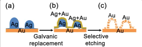
[image:2.595.305.538.607.685.2]Results and discussion 3D nanoporous gold structures
Figure 1 shows a schematic diagram that the 3D-NPG ultra-thin nanostructures were formed by the GRR and se-lective etching processes. First, hemispherical silver nanois-lands are electrodeposited on a cathodic Au substrate
Figure 1Schematic diagram depicting the three fabrication steps of 3D-NPG nanostructures. (a)Hemispherical silver nanoislands,
without any templates or surfactants, as reported in a pre-vious study (Figure 1a) [26]. Secondly, the silver atoms on the nanostructure surface are replaced by gold atoms, according to the GRR process, when the nanostructure is immersed in a 50 μM HAuCl4· nH2O aqueous solution
without any external voltages, as shown in Figure 1b. The 3D-NPG nanostructures are formed by replicating the sil-ver nanoislands, after a selective etching of the silsil-ver cores (Figure 1c).
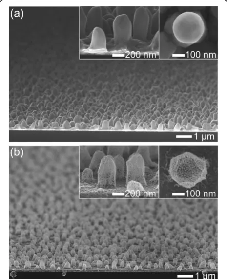
Figure 2a shows typical SEM images of the hemispher-ical silver islands (300 ± 28 nm in diameter) deposited on the Au-coated Si substrate. The silver nanoislands, which had an aspect ratio of approximately 2, were uniformly distributed over the entire substrate. Figure 2b exhibits the typical 3D-NPG nanostructures formed by the subsequent processes of GRR and selective etching. The GRR process occurred according to the following reaction of Equation 1 [20],
3Ag sð Þ þAuCl4‐ð Þaq →Au sð Þ þ3AgCl sð Þ
þCl‐ð Þaq ð1Þ
AuCl4− is reduced to one Au atom and silver is
oxi-dized to form AgCl. The GRR generates the small pits
on silver nanoislands (marked by the yellow arrows in Additional file 1: Figure S1a), which have relatively high surface energy [20,27]. During the GRR process, gold ions are expected to be reduced forming facetted surfaces because gold and silver phases have the same face-centered crystal structure, with lattice constants of 4.0786 and 4.0862 Å, respectively [20,27]. Thus, a thin Au facetted layer is formed replicating the surface of silver nanoislands and prevents underlying silver from reacting with AuCl4−ion.
The etching process occurs through the small pits, which play a role of the diffusion pathway for Ag+(as in-dicated by arrows in Additional file 1: Figure S1a-d). During the etching process, silver in the core and silver existing in the thin Au shell layer are selectively dissolved and resulted in the formation of hollow and nanoporous Au shell structure, i.e., 3D nanoporous gold structure. The nanoporosity might be ascribed that AuCl4− is reduced to
one gold atom at the expense of three silver atoms, according to Equation 1. As the surface area and surface energy increase with further etching of silver, the recon-struction of the pore morphology occurs via Ostwald ripening process [27,28].
GRR in ultra-dilute electrolyte led to the formation of uniform and ultra-thin 3D-NPG nanostructures because the low concentration of the electrolyte decreased the concentration gradient between the cathodic surface and solution and formed a thick double layer (diffusive re-gion) leading to a slow reaction-rate of galvanic replace-ment [26,29,30]. Therefore, for the ultra-dilute electrolyte (50μM), the GRR occurred only on the surface of the sil-ver islands and after 24 h resulted in the formation of the isolated 3D-NPG on the substrate (see yellow dotted lines in Additional file 1: Figure S2a). With further time up to 48 h, the GRR occurred over the entire bottom surface as well as the silver nanoislands, forming the interconnected 3D-NPG (see Additional file 1: Figure S2b). However, with the further GRR time up to 72 h, the nanopores of 3D-NPG gradually disappeared, and thick gold walls with smooth surfaces were produced by oxidizing silver in the core (Additional file 1: Figures S1d and S1h). In contrast, when the electrolyte concentration was increased to 200 μM HAuCl4 · nH2O, the initial hemispherical shape was
[image:3.595.57.290.396.682.2]not maintained and became rough because the GRR oc-curred faster and severely (Additional file 1: Figure S3). In addition, AgCl precipitates substantially formed on the nanostructure surface (see the yellow arrows marked in Additional file 1: Figure S3).
Figure 3 shows the typical bright field TEM (BFTEM) image and selected area electron diffraction (SAED) pat-tern of 3D-NPG shown in Figure 2b. The SAED shows a ring-like pattern indicating that the 3D-NPG has a face-centered-cubic polycrystalline structure. The ring pat-terns are indexed to be (111), (200), (220), (311), (222),
(400), and (331) reflection planes from the center, in sequence. And it is noted that the 3D-NPG is composed of many nanopores (less than several tens of nanometers in diameter).
3D-nanoshell gold structures
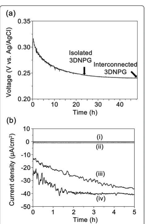
As shown in the open circuit voltage variation with the GRR time up to 48 h (see Figure 4a), the voltage slowly decreased from 0.32 to 0.24 V. This suggests that the GRR might be controlled by applying an external bias voltage to the cathodic substrate. When the bias voltage was 0.2 V, the porosity of the final nanostructure was almost identical to that of 3D-NPG nanostructure, and the formation of AgCl was reduced (Figures 4b-ii and S4). Accordingly, the porosity of the 3D-NPG was con-trolled by applying the bias voltage in the range of 0.2 to−0.62 V. With the increase of bias voltage, the current density increased, as shown in Figure 4b. The increase of current density implied more supply of electrons which are needed for the reduction of AuCl4− ions. Figure 5
[image:4.595.57.292.90.208.2]shows that the increase of bias voltage decreased poros-ity and resulted in the formation of nanoshell gold struc-tures. It is presumed that the bias voltage plays a role of supplying electrons and reducing the expense of silver
[image:4.595.57.292.312.675.2]Figure 3TEM images of the 3D-NPG nanostructure. (a)BFTEM image and(b)SAED pattern.
Figure 4Variation of open circuit voltage (OCV) and current density. (a)Variation of OCV during GRR process in a 50μM HAuCl4· nH2O electrolyte and(b)variations of current densities with the bias voltage (V) of (i) OCV, (ii) 0.2, (iii)−0.3, and (iv)−0.64 during the GRR process, respectively.
[image:4.595.305.538.387.677.2]atoms during the GRR process because AuCl4− ions are
reduced to one gold atom at the expense of three elec-trons supplied by silver, according to Equation 1. Thus, the consumption of silver atoms decreases, and then the porosity decreases when electrons are externally pro-vided. This process is not only affected by the chemical reaction for galvanic replacement, but also the underpo-tential deposition of a metallic adlayer onto a different metallic substrate [30].
3D-nanostructures of platinum and palladium
The GRR process was utilized to synthesize 3D nanopor-ous platinum and 3D-nanoshell palladium structures, as shown in Figure 6. Figure 6a shows the typical SEM im-ages of ultra-thin 3D nanoporous platinum nanostructures produced by the GRR process in a 50μM H2PtCl6· xH2O
solution and a selective etching process. The redox reac-tion of silver and PtCl62−occurs following Equation 2 [24].
The 3D nanoporous platinum structures had smaller nanopores and face-centered cubic crystal structure, as indexed by TEM and electron diffraction pattern analyses (Additional file 1: Figure S5).
4Ag sð Þ þPtCl62‐ð Þaq →Pt sð Þ þ4Agþð Þaq
þ6Cl‐ð Þaq ð2Þ
With a similar vein, 3D-nanoshell palladium nano-structures were fabricated by the GRR process in 100 μM Na2PdCl4 (bias voltage of −0.6 V) and a selective
etching process, as shown in Figure 6b. It was noted that the 3D-nanoshell palladium structures had thick shells rather than porous structure with the help of bias voltage, as discussed above.
[image:5.595.305.538.284.642.2]SERS of 3D nanoporous gold structures
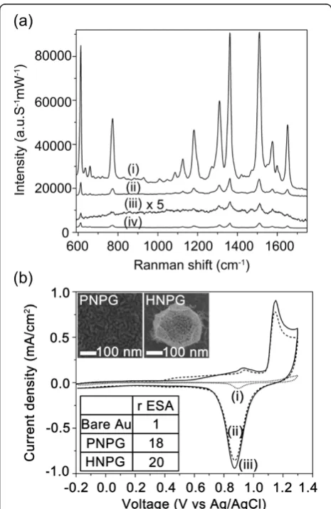
[image:5.595.56.291.375.686.2]Figure 7a shows the SERS spectra of R6G adsorbed on the 3D-NPG nanostructures and PNPG film with the R6G concentration in the range of 10−6 to 10−8 M. All
Figure 6Tilted SEM images of 3D nanoporous platinum and 3D-nanoshell palladium nanostructures.The insets denote the tilted and top-view SEM images with a higher magnification, respectively.
the SERS peaks for 3D-NPG nanostructures are clearly dis-tinguished by 633 nm laser and assigned to the characteris-tics of R6G Raman spectra [31,32]. In comparison, the SERS intensity of R6G on PNPG film is approximately 40 times lower than that on 3D-NPG nanostructures, even though the surface areas of both nanostructures are almost similar to each other, according to rESA measurement (the below inset of Figure 7b). The rESA was evaluated by cyclic voltammograms in N2-saturated 0.1 M H2SO4, as shown in
Figure 7b. The similar surface areas of 3D-NPG and PNPG are due to the less formation of nanopores around 3D hollow nanostructures, as shown in the inset of Figure 7b. Generally, the higher SERS intensity is known to come from nanpore size, ratios of ligaments to nanopores, and surface roughness [12,13]. However, in the present study, the difference of pore sizes between 3D-NPG and PNPG was not so large, approximately 3 nm. This suggests that the SERS enhancement for 3D-NPG nanostructures might be due to other effects. One possible reason is supposed to be the polygonal edges of 3D-NPG (see the inset of Figure 7b). Previously, it was reported that high index gold nanocrystals exhibit more efficient SERS activity than spherical gold nanocrystals and an electromagnetic field en-hancement effect arises because the electric field localizes more easily at the edges of nanocrystals [33]. And, the SERS spectra of 10−6 M R6G were measured at random points over the whole substrate. The SERS enhancement was highly reproducible at random five points over the whole substrate, as shown in the SERS spectra (Additional file 1: Figure S6). Thus, ultra-thin 3D-NPG nanostructures were easily fabricated by the bottom-up process providing a uniform SERS substrate without hot spots.
Conclusions
We suggest a facile and low-cost process of fabricating 3D hollow metallic nanostructures. The 3D hollow nanostruc-tures of gold, platinum, and palladium were uniformly synthesized using sacrificial silver nanostructures on a substrate. As the porosity of the 3D hollow nanostructures was able to be controlled by the bias voltage between the cathode and the anode, the nanoporous and nanoshell structures could be alternatively synthesized. In compari-son with PNPG nanostructures, the 3D-NPG nanostruc-tures were proved to be a superior SERS substrate with a higher enhancement of SERS intensity. The template-free electrodeposition and GRR process based on ultra-dilute electrolytes are expected to be utilized for further develop-ment of various 3D hollow porous nanostructures.
Additional file
Additional file 1:SEM and TEM images.SEM and TEM images of 3D nanostructures including SERS spectra for R6G molecules.
Competing interests
The authors declare that they have no competing interests.
Authors’contributions
SHP performed the synthesis and characterization of various noble nanostructures and drafted the manuscript. JGS carried out the measurement of SERS property. TGL and SYH participated in the analysis of SERS property. JWK analyzed the electrochemical behavior. HMP contributed to the analysis of the crystal structures of various noble nanostructures. JYS organized this work and finalized the manuscript. All authors read and approved the final manuscript.
Acknowledgements
We would like to acknowledge the financial support from the R&D Convergence Programs of MSIP (Ministry of Science, ICT and Future Planning), ISTK (Korea Research Council for Industrial Science and
Technology) (Grant B551179-13-01-03), and KRCF (Korea Research Council of Fundamental Science and Technology) (Grant 13-2-KIST) of Republic of Korea.
Author details
1Korea Research Institute of Standard and Science, Daejeon 305-340,
Republic of Korea.2Department of Chemistry, Korea Advanced Institute of Science and Technology, Daejeon 305-701, Republic of Korea.3Department of Chemistry, Chungbuk National University, Chungbuk 361-763, Republic of Korea.4Department of Nanochemistry, Gachon University, Gyeonggi 461-701, Republic of Korea.5Korea University of Science and Technology, Daejeon 305-350, Republic of Korea.
Received: 19 September 2014 Accepted: 4 December 2014 Published: 16 December 2014
References
1. Meng F, Ding Y:Sub-micrometer-thick all-solid-state supercapacitors with high power and energy densities.Adv Mater2011,23:4098–4102. 2. Nagle LC, Rohan JF:Nanoporous gold anode catalyst for direct
borohydride fuel cell.Int J Hydrogen Energy2011,36:10319–10326. 3. Kneipp K, Wang Y, Kneipp H, Perelman LT, Itzkan I:Single molecule
detection using surface-enhanced Raman scattering (SERS).Phys Rev Lett
1997,78:1667–1670.
4. Bae JH, Han J-H, Chung TD:Electrochemistry at nanoporous interfaces: new opportunity for electrocatalysis.Phys Chem Chem Phys2014, 14:448–463.
5. Zhang J, Li CM:Nanoporous metals: fabrication strategies and advanced electrochemical applications in catalysis, sensing and energy systems.
Chem Soc Rev2012,41:7016–7031.
6. Park S, Kim HC, Chung TD:Electrochemical analysis based on nanoporous structures.Analyst2012,137:3891–3903.
7. Wi J-S, Tominaka S, Uosaki K, Nagao T:Porous gold nanodisks with multiple internal hot spots.Phys Chem Chem Phys2012,14:9131–9136. 8. Campbell CT, Parker SC, Starr DE:The effect of size-dependent nanoparticle
energetics on catalyst sintering.Science2002,298:811–814. 9. Yoo S-H, Park S:Platinum-coated, nanoporous gold nanorod arrays:
synthesis and characterization.Adv Mater2007,19:1612–1615. 10. Shin T-Y, Yoo S-H, Park S:Gold nanotubes with a nanoporous wall: their
ultrathin platinum coating and superior electrocatalytic activity toward methanol oxidation.Chem Mater2008,20:5682–5686.
11. Yoo S-H, Liu L, Cho SH, Park S:Platinum-coated porous gold nanorods in methanol electrooxidation: dependence of catalytic activity on ligament size.Chem Asian J2012,7:2937–2941.
12. Qian LH, Yan XQ, Fujita T, Inoue A, Chen MW:Surface enhanced Raman scattering of nanoporous gold: smaller pore sizes stronger enhancements.Appl Phy Lett2007,90:153120.
13. Lang XY, Chen LY, Guan PF, Fujita T, Chen MW:Geometric effect on surface enhanced Raman scattering of nanoporous gold: Improving Raman scattering by tailoring ligament and nanopore ratios.Appl Phy Lett
2009,94:213109.
14. Erlebacher J, Aziz MJ, Karma A, Dimitrov N, Sieradzki K:Evolution of nanoporosity in dealloying.Nature2001,410:450–453.
[image:6.595.305.541.381.739.2]16. Nishio K, Masuda H:Anodization of gold in oxalate solution to form a nanoporous black film.Angew Chem Int Ed2011,50:1603–1607. 17. Wan Y, Yang H, Zhao D:Host-guest chemistry in the synthesis of ordered
nonsiliceous mesoporous materials.Acc Chem Res2006,39:423–432. 18. Lu L, Capek R, Kornowski A, Gaponik N, Eychmüller A:Selective fabrication of
ordered bimetallic nanostructures with hierarchical porosity.Angew Chem Int Ed
2005,44:5997–6001.
19. Lu L, Eychmüller A, Kobayashi A, Hirano Y, Yoshida K, Kikkawa Y, Tawa K, Ozaki Y:Designed fabrication of ordered porous Au/Ag nanostructured films for surface-enhanced Raman scattering substrates.Langmuir2006, 22:2605–2609.
20. Au L, Lu X, Xia Y:A comparative study of galvanic replacement reactions involving Ag nanocubes and AuCl2−or AuCl4−.Adv Mater2008,
20:2517–2522.
21. Sattayasamitsathit S, Gu Y, Kaufmann K, Minteer S, Polskyc R, Wang J: Tunable hierarchical macro/mesoporous gold microwires fabricated by dual-templating and dealloying processes.Nanoscale2013,5:7849–7854. 22. Yamauchi Y, Suzuki N, Radhakrishnan L, Wang L:Breakthrough and future:
nanoscale controls of compositions, morphologies, and mesochannel orientations toward advanced mesoporous materials.Chem Rec2009, 9:321–339.
23. Wang L, Yamauchi Y:Metallic nanocages: synthesis of bimetallic Pt−Pd hollow nanoparticles with dendritic shells by selective chemical etching.
J Am Chem Soc2013,135:16762–16765.
24. Chen H-M, Liu R-S, Lo M-Y, Chang S-C, Tsai L-D, Peng Y-M, Lee J-F:Hollow platinum spheres with nano-channels: synthesis and enhanced catalysis for oxygen reduction.J Phys Chem C2008,112:7522–7526.
25. Jiao Y, Ryckman JD, Ciesielski PN, Escobar CA, Jennings GK, Weiss SM: Patterned nanoporous gold as an effective SERS template.
Nanotechnology2011,22:295302.
26. Park SH, Shin HS, Kim YH, Park HM, Song JY:Template-free and filamentary growth of silver nanowires: application to anisotropic conductive transparent flexible electrodes.Nanoscale1864–1869,2013:5. 27. Sun Y:Silver nanowires–unique templates for functional nanostructures.
Nanoscale2010,2:1626–1642.
28. Roosen AR, Carter WC:Simulations of microstructural evolution: anisotropic growth and coarsening.Phys A1998,261:232–247.
29. Kanai N:Electroplating-Basic Principles, Processes and Practice.Amsterdam: Elsevier; 2006. ch.4-5, 98–107,150-153.
30. Herrero E, Buller LJ, Abruña HD:Underpotential deposition at single crystal surface of Au, Pt Ag and other materials.Chem Rev1897–1930, 2001:101.
31. Sun Z, Li Y, Wang Y, Chen X, Zhang J, Zhang K, Wang Z, Bao C, Zeng J, Zhao B, Yang B:Three-dimensional colloidal crystal-assisted lithography for two-dimensional patterned arrays.Langmuir2007,23:10725–10731. 32. Jensen L, Schatz GC:Resonance Raman scattering of rhodamine 6G as calculated using time-dependent density functional theory.J Phys Chem A
2006,110:5973–5977.
33. Hong JW, Lee S-U, Lee YW, Han SW:Hexoctahedral Au nanocrystals with high-index facets and their optical and surface-enhanced Raman scattering properties.J Am Chem Soc2012,134:4565–4568.
doi:10.1186/1556-276X-9-679
Cite this article as:Parket al.:Galvanic synthesis of three-dimensional and hollow metallic nanostructures.Nanoscale Research Letters20149:679.
Submit your manuscript to a
journal and benefi t from:
7 Convenient online submission 7 Rigorous peer review
7 Immediate publication on acceptance 7 Open access: articles freely available online 7 High visibility within the fi eld
7 Retaining the copyright to your article