Metal contact to SiC is not easy to modulate since the contact can be influenced by the metal, the termination of the SiC, the doping, and the fabrication process. In this work, we introduce a method by inserting a thin Al2O3layer between metal and SiC to solve this problem simply but effectively. The Al2O3/n-SiC interface composition was obtained with X-ray photoemission spectroscopy, and the electrical properties of subsequently deposited metal contacts were characterized by current–voltage method. We can clearly demonstrate that the insertion of Al2O3 interfacial layer can modulate the current density effectively and realize the transfer between the Schottky contact and ohmic contact.
Keywords:Contact resistance, Schottky barrier height, SiC, Atomic layer deposition
Background
Silicon carbide is a promising material for numerous electronic applications due to its wide bandgap, high breakdown electric field, high thermal conductivity, and high saturation velocity [1]. These excellent properties make SiC suitable for high-temperature, high-power, and high-frequency applications. For high-performance and high-frequency devices in these applications, metal/SiC contact plays very important roles. However, the trad-itional method for fabricating Schottky contact and ohmic contact are so different, and it will unavoidably add to the processing difficulty and cost [2].
The Schottky barrier height (SBH) is the key factor that determines whether the electrical behavior is an ohmic contact or Schottky contact: a low SBH is neces-sary to create a good ohmic contact, while a large SBH is required to form a good Schottky contact. According to the thermionic emission model [3], the direct reflec-tion of the SBH is the reverse current density, and there-fore, by controlling the Schottky barrier height, we can modulate the current density and acquire the needed contact type without modifying the fabrication process.
In a previous study, Connelly et al. [4] have raised a method to reduce the SBH of the metal/Si contact by using a thin Si3N4 through the creation of a dielectric
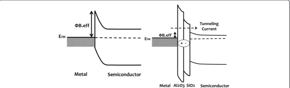
dipole [5]. Similar researches have been dedicated to the study of the SBH modulation on Ge [6-9], GaAs [10], InGaAs [10,11], GaSb [12], ZnO [13], and organic ma-terial [14] by inserting different dielectrics or bilayer di-electrics. According to the bond polarization theory [15], an electronic dielectric dipole is formed between the inserted insulator and semiconductor native oxide which results in a shift of the SBH, as Figure 1 depicts. The ori-gin of the dipole formation at the dielectric/SiO2
inter-face is described in Kita’s model [16], and in this model, the areal density difference of oxygen atoms at the di-electric/SiO2interface is the driving force to form the
di-pole. Since the areal density of oxygen atoms (σ) of Al2O3is larger than that of SiO2, theσ difference at the
interface will be compensated by oxygen transfer from the higher-σ to the lower-σ oxide which creates oxygen vacancies in the higher-σ oxide (Al2O3) and negatively
charged centers in the lower-σoxide (SiO2), and the
cor-responding direction of the dipole moment is from SiO2
to Al2O3. As a result, this dipole is a positive dipole
which can reduce the SBH and therefore increases the current density. As the thickness of the inserted insula-tor increases, it becomes more difficult for the current to tunnel through the insulator, and the tunneling bar-rier is the dominant factor of the total barbar-rier height, which decreases the current density in the end.
In this work, we demonstrate the modulation of the current density in the metal/n-SiC contact by inserting a * Correspondence:[email protected];[email protected]
State Key Laboratory of ASIC and System, Department of Microelectronics, Fudan University, Shanghai, 200433, China
thin Al2O3 layer into a metal-insulator-semiconductor
(MIS) structure. Al2O3is chosen as the interfacial
insu-lator for its large areal oxygen density (σ) which means that the formation of dipole is much stronger and shifts the SBH more effectively than that induced by other in-sulators based on the bond polarization theory [15] and Kita’s model [16]. As for the choice of metal, aluminum (Al) is suitable due to its low work function (4.06 to 4.26 eV) for the investigations of the Fermi level shift toward the conduction band of SiC (electron affinity = 3.3 eV).
The analysis of the Al2O3/SiC interface during the
formation of Al2O3was obtained with X-ray
photoemis-sion spectroscopy (XPS), and the electrical properties of Al/ Al2O3/SiC with different thicknesses of the inserted
Al2O3 were characterized by current–voltage (I-V)
method. Since the current density as well as the contact resistance was found to be sensitive to the Al2O3
thick-ness, we carefully varied the Al2O3thickness from 0.97
to 6.3 nm and finally have acquired the experiment re-sults that can describe the modulation of current dens-ity by changing the thickness of the insulator.
Methods
We prepared an Al/Al2O3/SiC MIS structure on n-type
C-terminated 6H-SiC with a carrier concentration of 1 × 1016 cm−3 epitaxially deposited by metal-organic chem-ical vapor deposition. Firstly, samples were cleaned in solutions of detergent, H2SO4/H2O (1:4), NH4OH/
H2O2/H2O (1:1:5), and HCl/H2O2/H2O (1:1:6), and
treated with HF/H2O (1:50) solution, followed by rinsing
in deionized water to remove native oxide at the surface. Secondly, the Al2O3 film was then deposited using
trimethylaluminum and H2O as precursors at 200°C by
atomic layer deposition (ALD). Various thicknesses of Al2O3 were achieved by changing the number of ALD
cycles, and nine samples were prepared with the Al2O3
thicknesses ranging from 0.97 to 6.3 nm. Finally, for all the samples, 100-nm Al was evaporated onto the Al2O3
surface as the top contact through shadow masks, and back side contact was also formed through the evapor-ation of Al. The MIS structure is depicted in Figure 2a. Figure 2b is a cross-sectional transmission electron microscope (TEM) image of Al/Al2O3/SiC which
pre-sents that Al2O3 was uniformly deposited as a fully
amorphous film.
In order to determine the generation of SiO2 and the
content ratio of SiO2 and SiC, the XPS method is used.
[image:2.595.59.539.90.236.2] [image:2.595.306.538.546.685.2]XPS experiments were carried out on a RBD-upgraded PHI-5000C ESCA system (PerkinElmer, Waltham, MA, USA) with Mg Kαradiation (hν= 1,253.6 eV), and the base pressure of the analyzer chamber was about 5 × 10⁻⁸Pa. Ar ion sputtering was performed to clean the sample in order to alleviate the influence of carbon element in the air. Samples were directly pressed to a self-supported disk (10 × 10 mm) and mounted on a sample holder, then transferred into the analyzer chamber. The whole spectra (0 to 1,100 eV) and the narrow spectra of Si 2p, O 1s, C 1s, and Al 2p with much high resolution were both recorded, and binding energies were calibrated using the Figure 1A schematic band diagram of a shift in the metal/semiconductor’s high barrier height.This is done by forming an electronic dielectric dipole between the insulator and the oxide of semiconductor in accordance with the bond polarization theory.
Figure 2Schematic diagram of MIS structure and cross-sectional TEM of Al/Al2O3/SiC.(a) A schematic diagram of the MIS structure.
(b) The cross-sectional TEM of the Al/Al2O3/SiC contact, showing that
Results and discussion
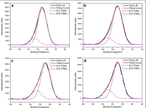
Figure 3 describes the Si 2p3 core-level spectra of the four samples with the Al2O3 thicknesses of 1.3, 1.98,
2.79, and 3.59 nm, respectively. It is clear that the Si 2p3 spectrum can be fitted with two Gaussian peaks which correspond to Si-C bonds (100.9 eV, FWHM = 2.27 eV)
of SiO2 oxidized by Al2O3 reaches an increase at the
Al2O3 thickness of 1.98 nm. The content ratio of SiO2/
SiC stays nearly at 17% in the Al2O3film with the
thick-ness beyond 1.98 nm. However, the content ratio of SiO2/SiC increases to 21.58% at the Al2O3thickness of
2.32 nm and almost remains around 21.89% at the Al2O3 thickness of 3.59 nm and thicker samples. The
Figure 3Si 2pXPS spectra of samples 1, 2, 3, and 4 with varying thicknesses.(a) Sample 1 with Al2O3thickness of 1.3 nm. (b) Sample 2
with Al2O3thickness of 1.98 nm. (c) Sample 3 with Al2O3thickness of 2.32 nm. (d) Sample 4 with Al2O3thickness of 3.59 nm. The black solid line
content ratio of SiO2/SiC rises by about 24% from the
1.98-nm sample to the 2.32-nm sample, which is pos-sibly due to the fact that the well-oxidized SiO2 begins
to generate when the Al2O3 thickness is thicker than
1.98 nm.
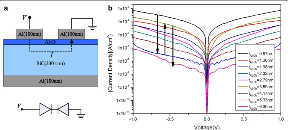
TheI-Vcharacteristics of the Al/Al2O3/SiC MIS
struc-ture were measured by the circuit connections of the back-to-back Schottky diode as illustrated in Figure 5a. One advantage of the back-to-back diode measurement is that the large resistance contributed from the series resistance and the large resistance caused by the sub-strate can be eliminated. Another advantage is that both
[image:4.595.306.538.87.260.2]in positive and negative biasing, only the reverse current is measured, and fortunately, the change in reverse sat-uration current reflects the characteristic of the contact where maximum reverse saturation current is desired for ohmic contacts.
Figure 5b shows the I-V characteristics of an Al/ Al2O3/SiC diode with different thicknesses of Al2O3.
Re-verse bias current first decreases due to the increase of Al2O3 thickness which can block off the current and
then has its minimum at the thickness of 1.98 nm which is suitable for the Schottky contact. When keeping on in-creasing the thickness, the reverse current rises since the formation of positive dipole between Al2O3and SiO2pulls
Figure 4The four samples’content ratio of SiO2and SiC.The
[image:4.595.56.292.89.260.2]content ratio transfers to the area ratio of Si-O bond’s fitting curve and Si-C bond’s fitting curve.
Figure 5Illustration of the back-to-back diode measurement setup and back-to-back Al/Al2O3/SiC diode measurements.(a) Illustration
of the back-to-back diode measurement setup where only the reverse current is measured. (b) Back-to-back Al/Al2O3/SiC diode measurements
demonstrating the effective modulation of current density by the thickness of Al2O3.
Figure 6Schematic ofRCversustoxfor MIS contact by inserting
[image:4.595.59.538.476.693.2]When the thickness of Al2O3 is thinner than 1.98 nm,
the dipole was not completely formed, and as a result, the inserted insulator blocks the current. In this range, along with the increase of the insulator, the contact re-sistance increases. According to the XPS result discussed above, the electronic dielectric dipole begins to create at the thickness of 1.98 nm. The formation of the dipole at the interface reduces the tunneling barrier and then raises the current across the contact in a reasonable re-gion. Figure 6 shows the RC versus the thickness of
Al2O3, which provided that the contact resistance is
modulated by the thickness of the insulator. It is inter-esting to find that there exists a trough because of the trade-off between a reduced barrier by the electronic di-electric dipole and an increased tunneling resistance by the accretion of the insulator’s thickness.
Conclusions
In this work, we successfully realize the modulation of current density at the metal/SiC contact by inserting a thin Al2O3layer between the metal and semiconductor.
By varying the thickness of Al2O3, we can acquire the
ideal current density and contact resistance based on our demands and achieve a transfer between Schottky contact and ohmic contact. The mechanism appears to be the coaction of a positive dielectric dipole decreasing the barrier and the tunneling resistance increasing the barrier. Consequently, this is a promising method to in-crease the performance of SiC electronic applications.
Competing interests
The authors declare that they have no competing interests.
Authors’contributions
SZ carried out the sample fabrication and drafted the manuscript. WY carried out the device measurements. PZ and HL participated in the manuscript writing and results discussion. QS and DZ participated in the design of the study and performed the statistical analysis. All authors read and approved the final manuscript.
Acknowledgments
This work was supported by the NSFC (61076114, 61106108, and 51172046), the Shanghai Educational Develop Foundation (10CG04), SRFDP
(20100071120027), the Fundamental Research Funds for the Central Universities, and the S&T Committee of Shanghai (1052070420).
Parthasarathy S, Barnett J, Majhi P, Wallace RM, Kim J, Jammy R:CMOS band-edge schottky barrier heights using dielectric-dipole mitigated (DDM) metal/Si for source/drain contact resistance reduction. InDigest of Technical Papers - Symposium on VLSI Technology.Piscataway: IEEE; 2009:104. 6. Lin JYJ, Roy AM, Nainani A, Sun Y, Saraswat KC:Increase in current density for metal contacts to n-germanium by inserting TiO2interfacial layer to reduce Schottky barrier height.Appl Phys Lett2011,98:092113. 7. Kobayashi M, Kinoshita A, Saraswat K, Wong HSP, Nishi Y:Fermi level
depinning in metal/Ge Schottky junction for metal source/drain Ge metal-oxide-semiconductor field-effect-transistor application.J Appl Phys
2009,105:023702.
8. Nishimura T, Kita K, Toriumi A:A significant shift of Schottky barrier heights at strongly pinned metal/germanium interface by inserting an ultra-thin insulating film.Appl Phys Express2008,1:051406.
9. Lieten RR, Degroote S, Kuijk M, Borghs G:Ohmic contact formation on n-type Ge.Appl Phys Lett2008,92:022106.
10. Hu J, Saraswat KC, Wong HSP:Metal/III-V Schottky barrier height tuning for the design of nonalloyed III-V field-effect transistor source/drain contacts.J Appl Phys2010,107:063712.
11. Hu J, Saraswat KC, Wong HSP:Experimental demonstration of In0.53Ga0.47As field effect transistors with scalable nonalloyed source/ drain contacts.Appl Phys Lett2011,98:062107.
12. Yuan Z, Nainani A, Sun Y, Lin JY, Pianetta P, Saraswat KC:Schottky barrier height reduction for metal/n-GaSb contact by inserting TiO2interfacial layer with low tunneling resistance.Appl Phys Lett2011,98:172106. 13. Krajewski TA, Luka G, Giereltowska S, Zakrzewski AJ, Smertenko PS, Kruszewski P,
Wachnicki L, Witkowski BS, Lusakowska E, Jakiela R, Godlewski M, Guziewicz E:
Hafnium dioxide as a passivating layer and diffusive barrier in ZnO/Ag Schottky junctions obtained by atomic layer deposition.Appl Phys Lett2011,
98:263502.
14. Liu ZH, Kobayashi M, Paul BC, Bao ZN, Nishi Y:Contact engineering for organic semiconductor devices via Fermi level depinning at the metal-organic interface.Phys Rev B2010,82:035311.
15. Tung R:Formation of an electric dipole at metal–semiconductor interfaces.Phys Rev B2001,64:205310.
16. Kita K, Toriumi A:Intrinsic origin of electric dipoles formed at high-k/SiO2 interface. InTechnical Digest - International Electron Devices Meeting.
Piscataway: IEEE; 2008:1–4.
17. Wagner CD:Handbook of X-ray Photoelectron Spectroscopy.Eden Prairie: Physical Electronics Division, Perkin-Elmer Corporation; 1979.
18. Li HF, Dimitrijev S, Sweatman D, Harrison HB, Tanner P, Feil B:Investigation of nitric oxide and Ar annealed SiO2/SiC interfaces by x-ray
photoelectron spectroscopy.J Appl Phys1999,86:4316.
19. Őnneby C, Pantano CG:Silicon oxycarbide formation on SiC surfaces and at the SiC/SiO2interface.J Vac Sci Technol A1997,15:1597.
20. Schroder D:Semiconductor Material and Device Characterization.3rd edition. Hoboken: Wiley; 2006.
doi:10.1186/1556-276X-8-116