N A N O E X P R E S S
Open Access
Evidence for formation of multi-quantum dots in
hydrogenated graphene
Chiashain Chuang
1,2, Reuben K Puddy
1, Malcolm R Connolly
1, Shun-Tsung Lo
3, Huang-De Lin
2, Tse-Ming Chen
4,
Charles G Smith
1*and Chi-Te Liang
2,3*Abstract
We report the experimental evidence for the formation of multi-quantum dots in a hydrogenated single-layer graphene flake. The existence of multi-quantum dots is supported by the low-temperature measurements on a field effect transistor structure device. The resulting Coulomb blockade diamonds shown in the color scale plot together with the number of Coulomb peaks exhibit the characteristics of the so-called‘stochastic Coulomb blockade’. A possible explanation for the formation of the multi-quantum dots, which is not observed in pristine graphene to date, was attributed to the impurities and defects unintentionally decorated on a single-layer graphene flake which was not treated with the thermal annealing process. Graphene multi-quantum dots developed around impurities and defect sites during the hydrogen plasma exposure process.
Keywords:Multi-quantum dots, Single-layer graphene flake, Coulomb peaks
Background
Graphene, a mono-layer of carbon atoms arranged in a honeycomb lattice, has extraordinary electrical proper-ties, such as the gapless linear dispersion [1-4]. In order to realize graphene-based nanoelectronic device applica-tions, many research groups tried to open the energy bandgap in the gapless linear dispersion in different ways, for instance, graphene nanoribbons [5,6] and bilayer gra-phene applied by the electric field [7-9]. Recently, hydro-genated graphene attracts a great deal of attention because of its bandgap behavior driven by the chemical functionalization [10-17]. The adsorbed atomic hydrogen atoms form three-dimensional C-H sp3 covalent bonds with carbon atoms by interrupting C-Csp2bonds, thus,
removing the conducting πbonds and opening a
band-gap [11,18,19]. In 2010, Singh and co-workers proposed that graphane could form natural host for graphene multi-quantum dots, clusters of vacancies in hydrogen sublattice [20]. According to the surface dynamics, ther-mally energetic hydrogen atoms adsorbed on graphene could be desorbed from the graphene surface or migrate
to the proper bonding sites or nucleate randomly (due to short diffusion length) to form dense islands of coexisting two-dimensional phases, C-H and C-C [14,20,21]. On the other hand, some reports proposed that the multi-quantum dots were unintentionally formed by impurities or defects in single-wall carbon nanotubes, which belong to the same honeycomb lattice as single-layer graphene [22-24].
In this study, we propose a possible explanation based on the aforementioned mechanism for the formation of multi-quantum dots on our single-layer graphene flake and supported by the low-temperature electrical trans-port measurements.
Methods
A graphene field-effect transistor (FET) device was fabri-cated for the investigation described in this work. A single-layer graphene flake, mechanically exfoliated from natural graphite, was deposited onto a highly doped Si substrate capped with a 300-nm-thick SiO2layer, serving
as a back gate [25]. Optical microscopy was used to lo-cate graphene flakes and confirms that it was a single layer shown in the inset to Figure 1a [1,25]. Two Ti/Au contacts (5/50 nm) were patterned, using e-beam lithog-raphy and lift-off processing, into the source and drain contacts. To retain the defects and impurities in the * Correspondence:[email protected];[email protected]
1Cavendish Laboratory, University of Cambridge, J. J. Thomson Avenue,
Cambridge CB3 0HE, UK
2Department of Physics, National Taiwan University, Taipei 106, Taiwan
Full list of author information is available at the end of the article
© 2012 Chuang et al.; licensee Springer. This is an Open Access article distributed under the terms of the Creative Commons Attribution License (http://creativecommons.org/licenses/by/2.0), which permits unrestricted use, distribution, and reproduction in any medium, provided the original work is properly cited.
graphene flakes to facilitate the formation of multi-quantum dots, the FET device was conditioned by the hydrogen plasma at conditions of power = 16 W and pressure = 0.2 Torr for 6 s without post-exfoliation annealing treatment [10,26].
An Oxford top-loading He4cryostat was used to carry out the two-terminal conductance measurements using standard AC lock-in technique at 77 Hz with a DC bias at the temperature range between 1.3 and 40 K.
Results and discussion
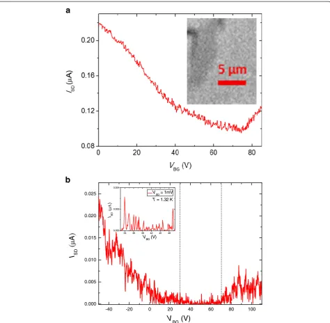
Figure 1a shows the source-drain current (ISD)
depend-ence on the back gate voltage (VBG) measured at the
charge neutrality point,VNP= 74 V, with a fixed
source-drain voltage VSD = 0.1 mV at T = 1.32 K before the
hydrogen plasma treatment. The charge neutrality point, which is far from the zero voltage, can be attributed to the hole-doping impurities left on the graphene flake [27,28]. Figure 1b shows the ISD-VBGmeasurement after
-40 -20 0 20 40 60 80 100
0.000 0.005 0.010 0.015 0.020 0.025
33 36 39 42 45 48 0.000
0.002 0.004
ISD
(μ
Α
)
VBG (V)
VSD = 1mV
T = 1.32 K
I SD
μ
A
VBG (V)
a
[image:2.595.62.537.88.552.2]b
Figure 1Source-drain current (ISD) dependence.(a)ISDmeasured atVBGfromVBG= 0 to 85 V at 1.32 K with a fixed source and drain voltage,
VSD= 0.1 mV, before hydrogen plasma treatment. The neutrality point voltageVNPis near 74 V. Inset: the optical image of a single-layer graphene
flake in contrast (b)ISDmeasured fromVBG=−50 to 110 V atT= 1.41 K with a fixed source and drain voltageVSD= 20 mV after hydrogen
plasma treatment. The Coulomb blockade oscillations occur between 30 and 50 V. Inset: the Coulomb peaks atT= 1.32 K with a fixed source and
hydrogen plasma treatment. Strong suppression of the source-drain current in the Coulomb blockade oscilla-tion region (between the dashed lines) with a fixed
source-drain voltage VSD = 20 mV at T = 1.41 K is
observed. To assure the Coulomb peaks in the Coulomb blockade oscillation region, we examined the Coulomb peaks with a fixedVSD= 1 mV at T = 1.32 K shown in
the inset to Figure 1b [29]. To further investigate the Coulomb blockade effect, the Coulomb blockade color scale plot of the conductance Gin aVBG-VSDplane was
[image:3.595.57.291.84.511.2]adopted for a better illustration of the existence of multi-quantum dots in our graphene flake sample; over-lapped diamond-shape pattern was expected.
Figure 2Color scale plot of the conductanceGversusVBGand
VSD.Shown at (a)T= 5 K and (b)T= 10 K. The back gate voltage
swept from 40 to 45 V at a step of 100 mV. The irregular feature of the Coulomb blockade region in Figure 2a suggests a multi-quantum dot formation.
41 42 43 44
0.00 0.04 0.08 0.12
40 41 42 43 44 45
0.00 0.02 0.04
G
(
μ
S)
VBG (V)
VSD = 9.5 mV VSD = 7.5 mV VSD = 6.5 mV T = 1.35 K
G
μ
S
VBG (V)
1.35 K 2.01 K 2.5 K
V SD = 9.5 mV
1 2 3 4 5 6 7
2 4 6 8 10 12
N
u
mb
er
o
f p
eak
s
Temperature (K)
a
b
Figure 3Temperature dependence and the number of Coulomb peaks.(a) Temperature dependence ofGversusVBG
(Coulomb oscillations) atVSD= 9.5 mV. Coulomb peaks are defined
by the ones that were consistently reproduced at differentVSD
whereas at the sameVBGas illustrated in the inset to Figure 3a.
(b) The number of Coulomb peaks as a function of the temperature
[image:3.595.306.538.85.442.2]corresponds to those depicted in Figure 3a.
Figure 4Color scale plot of the conductanceGversusVBGand
VSDatT=6.5 K.TheVBGwas increased from 40 to 45 V at a step
of 10 mV.
[image:3.595.305.540.518.694.2]Figure 2 shows a color scale plot of the differential
conductance G versus VBG and VSD at T = 5 K. The
overlap of Coulomb diamonds, so-called ‘Coulomb
shards’, was observed [30]. The Coulomb shards, which is also called stochastic Coulomb blockade, occurred due to the multi-quantum dots coupling in series during the carrier transport tunneling process [30-33]. Results of the measurements indicated that the multi-quantum dots formed in a two-dimensional manner. In other words, carriers could tunnel through the potential bar-riers of the quantum dots dispersed randomly. Coulomb shards disappeared while the temperature was increased
to T = 10 K as shown in Figure 2b, whereby it implied that thermal energy dominated the carrier transport be-havior rather than the multi-quantum dot Coulomb blockade tunneling [31-33].
The stochastic Coulomb blockade in the multi-quantum dot system is further supported by investiga-ting the temperature dependence of the number of the Coulomb peaks. Figure 3a shows the differential con-ductance as a function of VBGbetween 40.5 and 44.5 V
at different temperatures with a fixed VSD= 9.5 mV. To
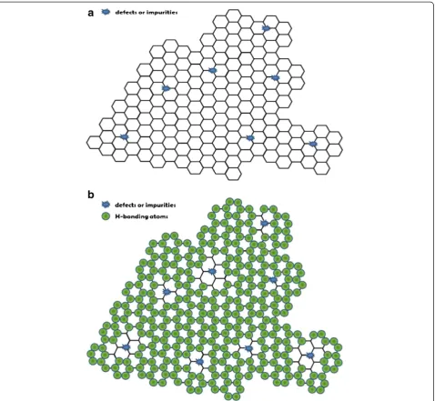
[image:4.595.61.540.88.529.2]distinguish the real Coulomb blockade peaks from the background noise, only reproducible peaks observed at Figure 5Schematics of defects and impurities and the formation of multi-quantum dots.(a) Schematic of defects and impurities on a
single-layer graphene flake before hydrogen plasma treatment. (b) Schematic of the formation of multi-quantum dots on hydrogen graphene. The
the same VBG with varying VSD (VSD = 6.5, 7.5, and
9.5 mV) are considered, shown in the inset to Figure 3a. The oscillations in Figure 3a are non-periodic, and the number of Coulomb peaks increases monotonically as the temperature is increased as shown in Figure 3b [22,30,31]. Both the aforementioned are the typical char-acteristics of the stochastic Coulomb blockade which suggests a formation of multi-quantum dots [31-34].
For a better visualization of the individual Coulomb dia-mond in the blockade region, the Coulomb diadia-mond color scale plot of the conductanceG with a better resolution
ΔVBG= 10 mV atT= 6.5 K was shown in Figure 4. The
clear Coulomb diamonds indicated that the charging ef-fect existed in our hydrogenated graphene system [35-37].
To justify the revealed overlapped Coulomb diamonds in our hydrogenated graphene system, a possible explanation for the formation of the multi-quantum dots is depicted in Figure 5. Without the post-exfoliation annealing process, the impurities or/and as-grown defects, shown as dots in Figure 5a, existed on the single-layer gra-phene flake [38-40]. In the vicinity of defects (mostly vacancies) or impurities, hydrogen passivated the edge carbon atoms on the vacancy sites or substituted im-purities by keeping the C-C sp2 bonding structure. In the defect/impurity-free regions, the C-H bonding transformed the C-C bonding from sp2into sp3 struc-ture [10,26]. After hydrogen plasma exposure, graphene multi-quantum dots were formed in the proximity of defects/impurities, depicted in Figure 5b. The asymmet-ric hydrogenated graphene quantum dot array could be treated as the sequential tunneling of charges through the two-dimensional (2D) array of single-layer graphene quantum dots [41]. The experimental results indicated that 2D multi-quantum dot array can be achieved by the hydrogenation of exfoliated graphene flakes expe-riencing no annealing process. More detailed funda-mental understanding of the origin of multi-quantum dots formed on the non-annealed hydrogenated graphene flakes can greatly promote the development of graphene-based multi-quantum dot devices for quantum computa-tion [42,43].
Conclusions
Two-dimensional multi-quantum dots can be realized on a mechanically exfoliated graphene flake followed by the hydrogen plasma treatment without executing post-exfoliation thermal annealing. The overlapped Coulomb blockade diamonds observed from the electrical measure-ments, as well as the monotonic increase of the number of Coulomb peaks with the ascending temperature, suggest the formation of two-dimensional multi-quantum dots that is unprecedented on the annealed graphene flakes with similar hydrogenation processes. Therefore, we suggest a defect (or vacancy) and impurity-related mechanism to
account for the formation of the multi-quantum dots dis-covered on our device. Further characterizations, such as AFM or SEM, on the atomic structure of un-annealed gra-phene layers might shed light on the origin of the quantum dot formation, whereas the degree of post-growth annealing could be utilized to engineer the quantum dots in terms of its size, density, shape, or charging states in a cost-effective way for quantum chip device applications.
Abbreviations
FET: field-effect transistor; 2D: two-dimensional.
Competing interests
The authors declare that they have no competing interests.
Authors’contributions
CC and RKP fabricated the samples. CC, RKP, and MRC performed the measurements. CC and HDL drafted the paper. TMC and STL provided models, interpretation, and possible explanations for the results. CGS and CTL coordinated the project. All authors read and approved the final manuscript.
Authors’information
CC obtained his B.Sc. degree in Physics at NCUE in 2006 and M.Sc. degree in Physics at NTNU in 2009. He is currently pursuing his Ph.D. degree in Physics at NTU. RKP is currently pursuing his Ph.D. degree at the Cavendish Laboratory, University of Cambridge. MRC is currently a postdoctoral research worker at the Cavendish Laboratory, University of Cambridge. STL obtained his B.Sc. degree at NTU in 2010 and is pursuing his Ph.D. degree at the Graduate Institute of Applied Physics, NTU. He won the Dr. An-Tai Chen Scholarship, Mr. Ming Kao Scholarship, and college students participating in special research project of Creative Award provided by the NSC in 2009. HDL obtained his B.S. degree at Chinese Culture University, Taiwan and his Ph.D. degree at Mississippi State University, USA, and currently works as a project engineer at Electronics Testing Center, Tao-Yuan, Taiwan (R.O.C). TMC obtained his B.Sc. degree and M.Sc. degree at NTU, Taiwan and obtained his Ph.D. degree at Cambridge University, UK. He is currently an assistant professor at the Department of Physics, NCKU. CGS obtained his Ph.D. degree at Cambridge University, UK and is currently a professor of Physics at Cambridge University, UK. CTL obtained his B.Sc. degree at NTU in 1990 and his Ph.D. degree in Physics at Cambridge University, UK in 1996 and is currently a professor of Physics at NTU. He is also a topical editor for Current Applied Physics.
Acknowledgments
This work was funded by the Initiative Research Cooperation among top universities between UK and Taiwan (grant no.: NSC 99-2911-I-002-126), the NSC (grant no: NSC 101-2923-M-002-003-MY3), and National Taiwan University (grant no: 101R7552-2). CC, TMC, and CTL would like to thank the hospitality of the Semiconductor Physics Group, Cavendish Laboratory. CTL thanks Tina Liang, Valen Liang, and Eva Liang for their support.
Author details
1Cavendish Laboratory, University of Cambridge, J. J. Thomson Avenue,
Cambridge CB3 0HE, UK.2Department of Physics, National Taiwan University,
Taipei 106, Taiwan.3Graduate Institute of Applied Physics, National Taiwan
University, Taipei 106, Taiwan.4Department of Physics, National Cheng Kung
University, Tainan 701, Taiwan.
Received: 26 June 2012 Accepted: 10 August 2012 Published: 16 August 2012
References
1. Geim AK, Novoselov KS:The rise of graphene.Nat Mate2007,6:183.
2. Castro Neto AH, Guinea F, Peres NMR, Novoselov KS, Geim AK:The
electronic properties of graphene.Rev Mod Phys2009,81:109.
3. Zhao S, Lv Y, Yang X:Layer-dependent nanoscale electrical properties of
graphene studied by conductive scanning probe microscopy.Nano Res Letts2011,6:498.
4. Ishikawa R, Bando M, Morimoto Y, Sandhu A:Doping graphene films via chemically mediated charge transfer.Nano Res Letts2011,6:111.
5. Han MY, Özyilmaz B, Zhang Y, Kim P:Energy band-gap engineering of
graphene nanoribbons.Phys Rev Lett2007,98:206805.
6. Son Y-W, Cohen ML, Louie SG:Energy gaps in graphene nanoribbons.
Phys Rev Lett2006,97:216803.
7. Castro EV, Novoselov KS, Morozov SV, Peres NMR, Santos JMB L, Nilsson J,
Guinea F, Geim AK, Castro Neto AH:Biased bilayer graphene:
semiconductor with a gap tunable by the electric field effect.Phys Rev Lett2007,99:216802.
8. Ohta T, Bostwick A, Seyller T, Horn K, Rotenberg E:Controlling the
electronic structure of bilayer graphene.Science2006,313:951.
9. Oostinga JB, Heersche HB, Liu X, Morpurgo AF, Vandersypen LMK:
Gate-induced insulating state in bilayer graphene devices.
Nature2008,7:151.
10. Elias DC, Nair RR, Mohiuddin TMG, Morozov SV, Blake P, Halsall MP, Ferrari AC,
Boukhvalov DW, Katsnelson MI, Geim AK, Novoselov KS:Control of graphene's
properties by reversible hydrogenation: evidence for graphane.
Science2009,323:610.
11. Sofo JO, Chaudhari AS, Barber GD:Graphane: a two-dimensional
hydrocarbon.Phys Rev B2007,75:153401.
12. Boukhvalov DW, Katsnelson MI:Chemical functionalization of graphene.
J Phys Condens Matter2009,21:344205.
13. Ryu S, Han YM, Maultzsch J, Heninz TF, Kim P, Steigerwald ML, Brus LE:
Reversible basal plane hydrogenation of graphene.Nano Lett2008,
8:4597.
14. Balog R, Jrgensen B, Nilsson L, Andersen M, Rienks E, Bianchi M, Fanetti M,
Lægsgaard E, Baraldi A, Lizzit S, Sljivancanin Z, Besenbacher F, Hammer B,
Pedersen TG, Hofmann P, Hornekær L:Bandgap opening in graphene
induced by patterned hydrogen adsorption.Nat Mater2010,9:315.
15. Dikin DA, Stankovich S, Zimney EJ, Piner RD, Dommett GHB, Evmenenko G,
Nguyen ST, Ruoff RS:Preparation and characterization of graphene oxide
paper.Nature2007,448:457.
16. Park S, Ruoff RS:Chemical methods for the production of graphenes.
Nat Nanotechnol2009,4:217.
17. Chuang C, Puddy RK, Lin H-D, Lo S-T, Chen T-M, Smith CG, Liang C-T:
Experimental evidence for efros-shklovskii variable range hopping in hydrogenated graphene.Solid State Commun2012,152:905.
18. Boukhvalov DW, Katsnelson MI, Lichtenstein AI:Hydrogen on graphene:
electronic structure, total energy, structural distortions and magnetism from first-principles calculations.Phys Rev B2008,77:035427.
19. Withers F, Russo S, Dubois M, Craciun MF:Tuning the electronic transport
properties of graphene through functionalisation with fluorine.Nano Res Letts2011,6:526.
20. Singh AK, Penev ES, Yakobson BI:Vacancy clusters in graphane as
quantum dots.ACS Nano2010,4:3510.
21. Luth H:Surface and Interfaces of Solid Materials. New York: Springer Press; 1995.
22. Suzuki M, Ishibashi M, Ida T, Aoyagi Y:Quantum dot formation in
single-wall carbon nanotubes.Jpn J Appl Phys1915,2001:40.
23. McEuen PL, Bockrath M, Cobden DH, Yoon Y-G, Louie SG:Disorder,
pseudospins, and backscattering in carbon nanotubes.Phys Rev Lett1999,
83:5098.
24. Zhou C, Kong J, Yenilmez E, Dai H:Modulated chemical doping of
individual carbon nanotubes.Science2000,290:1552.
25. Novoselov KS, Geim AK, Morozov SV, Jiang D, Zhang Y, Dubonos SV,
Grigorieva IV, Firsov AA:Electric field effect in atomically thin carbon films.Science2004,306:666.
26. Luo Z, Yu T, Kim K-J, Ni Z, You Y, Lim S, Shen Z, Wang S, Lin J:
Thickness-dependent reversible hydrogenation of graphene layers.
ACS Nano2009,3:1781.
27. Ponomarenko LA, Yang R, Mohiuddin TM, Katsnelson MI, Novoselov KS,
Morozov SV, Zhukov AA, Schedin F, Hill EW, Geim AK:Effect of a high-κ
environment on charge carrier mobility in graphene.Phys Rev Lett2009,
102:206603.
28. Connolly MR, Chiou KL, Smith CG, Anderson D, Jones GAC, Lombardo A,
Fasoli A, Ferrari AC:Scanning gate microscopy of current-annealed single
layer graphene.Appl Phys Lett2010,96:113501.
29. Ponomarenko LA, Schedin F, Katsnelson MI, Yang R, Hill EW, Novoselov KS,
Geim AK:Chaotic dirac billiard in graphene quantum dots.Science2008,
320:356.
30. Nazarov YV, Blanter YM:Quantum Transport Introduction to Nanoscience.
Cambridge: Cambridge University Press; 2009.
31. Ruzin IM, Chandrasekhar V, Levin EI, Glazman LI:Stochastic Coulomb
blockade in a double-dot system.Phys Rev B1992,45:13469.
32. Kemerink M, Molenkamp LW:Stochastic Coulomb blockade in a double
quantum dot.Appl Phys Lett1994,65:1012.
33. Ishibashi K, Suzuki M, Ida T, Aoyagi Y:Formation of coupled quantum dots
in single-wall carbon nanotubes.Appl Phys Lett1864,2001:79.
34. Notargiacomo A, Gaspare LD, Scappucci G, Mariottini G, Evangelisti F,
Giovine E, Leoni R:Single-electron transistor based on modulation-doped
SiGe heterostructures.Appl Phys Lett2003,83:302.
35. Guttinger J, Stampfer C, Fery T, Ihn T, Ensslin K:Transport through a
strongly coupled graphene quantum dot in perpendicular magnetic field.Nano Res Letts2011,6:253.
36. Liu XL, Hug D, Vandersypen MK:Gate-defined graphene double quantum
dot and excited state spectroscopy.Nano Letts2010,10:1623. 37. Molitor F, Dröscher S, Güttinger J, Jacobsen A, Stamper C, Ihn T, Ensslin K:
Transport through graphene double dots.Appl Phys Letts2009,94:222107.
38. Ishigami M, Chen JH, Cullen WG, Fuhrer MS, Williams EW:Atomic structure
of graphene on SiO2.Nano Lett2007,7:1643.
39. Schedin F, Geim AK, Morozov SV, Hill EW, Blake P, Katsnelson MI, Novoselov KS:
Detection of individual gas molecules adsorbed on graphene.Nat Mate 2007,6:652.
40. Hashimoto A, Suenage K, Gloter A, Urita K, Iijima S:Direct evidence for
atomic defects in graphene layers.Nature2004,430:870.
41. Joung D, Zhai L, Khondaker SI:Coulomb blockade and hopping
conduction in graphene quantum dots array.Phys Rev B2011,83:115323.
42. Nielsen MA, Chuang IL:Quantum Computation and Quantum Information.
Cambridge: Cambridge University Press; 2000.
43. Loss D, DiVincenzo DP:Quantum computation with quantum dots.Phys
Rev A1998,57:120.
doi:10.1186/1556-276X-7-459
Cite this article as:Chuanget al.:Evidence for formation of
multi-quantum dots in hydrogenated graphene.Nanoscale Research
Letters20127:459.
Submit your manuscript to a
journal and benefi t from:
7Convenient online submission
7Rigorous peer review
7Immediate publication on acceptance
7Open access: articles freely available online
7High visibility within the fi eld
7Retaining the copyright to your article