N A N O E X P R E S S
Electrostatically Shielded Quantum Confined Stark Effect Inside
Polar Nanostructures
Spilios Riyopoulos
Received: 5 December 2008 / Accepted: 12 May 2009 / Published online: 30 May 2009
Óto the authors 2009
Abstract The effect of electrostatic shielding of the polarization fields in nanostructures at high carrier densi-ties is studied. A simplified analytical model, employing screened, exponentially decaying polarization potentials, localized at the edges of a QW, is introduced for the ES-shielded quantum confined Stark effect (QCSE). Wave function trapping within the Debye-length edge-potential causes blue shifting of energy levels and gradual elimination of the QCSE red-shifting with increasing carrier density. The increase in the e-h wave function overlap and the decrease of the radiative emission time are, however, delayed until the ‘‘edge-localization’’ energy exceeds the peak-voltage of the charged layer. Then the wave function center shifts to the middle of the QW, and behavior becomes similar to that of an unbiased square QW. Our theoretical estimates of the radiative emission time show a complete elimination of the QCSE at doping densitiesC1020 cm-3, in quantitative agreement with experimental measurements.
Introduction
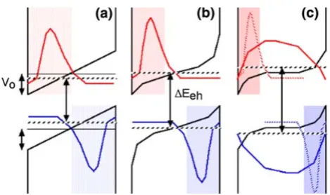
The presence of a strong, inherent polar electric field in GaN [1] causes the well-known quantum confined Stark effect [2–4] (QCSE) regarding carrier behavior inside a QW (Fig.1a). The separation of the center of charge between electron and hole wave functions, caused by the polar E-field, reduces mutual overlap and the related
emission probability. The lowering of the confined energy levels, relative to the unperturbed square QW, causes red-shifting of the emitted radiation during electron-hole recombination. This effect has been the subject of exten-sive perturbative [5] as well as non-perturbative analytic treatments [6–9], including excitonic effects [10–14]. In general earlier analytic theories neglected the modifications to the (intrinsic polar or externally applied)E-field caused by the charge separation and the resulting dielectric shielding, assuming in effect very low carrier densities.
At high carrier densities, charge separation and dipole field formation is sufficient to cause shielding of the intrinsic polarization E-field [15]. The resulting potential gradient across the QW is not uniform, and most of the potential drop is localized across charged layers formed at the edges of the QW (Fig.1b). The electric gradient scale is of the order of the Debye length. For densities near 1019cm-3 the Debye length shrinks down to nm-scale (Fig.1c), and the potential drop is mostly localized at the QW edges while the QW interior is nearly field-free (shielding of the intrinsic E-field). This constitutes the ES-shielded QCSE. It has been anticipated [16] that the shielding of the interior E-field would reduce or even eliminate the QCSE at densities 1019cm-3. Detailed numerical simulations, employing the self-consistent Pois-son–Schrodinger equations [17] have showed that a much higher than expected carrier density, near 1020cm-3, is required to eliminate the QCSE for QWs wider than 5 nm. This has been attributed to the persistence of carrier con-finement in the potential dips at the QW edges, even when the electric field is screened out from the middle. However, an analytic treatment examining the carrier behavior in the ES-shielded QCSE is so far lacking.
This study focuses in finding solutions for the confined carrier wave functions by solving the one-particle S. Riyopoulos (&)
Science Applications International Corporation, McLean, VA 22102, USA
Schrodingers’ equation. To gain insight the following simplifying assumptions are used: (a) The shielded poten-tial has exponenpoten-tially decaying profile on the Debye length *kDscale; (b) the peak-to-peak shielded voltage is a given
function of the carrier density and the intrinsic polarization strengthEo;and (c) excitonic effects are ignored.
The shielded potential results from a self-consistent solution of Poisson’s equation for point-like charges obeying Fermi statistics [15]. Neglecting the charge spreading of the carrier wave function is not too severe when the carrier localization length*kDis much smaller
than the QW widthL. When the Fermi level separation from the lowest occupied levels is much larger thanjT, i.e., for nearly Maxwellian distributions, the shielded potential is well approximated by a symmetric profile VshðxÞ ¼
VosinhðjDxÞ=sinhðjDL=2Þ: The exponentially decaying
profiles remain a reasonable approximation for Fermi– Dirac distributions in general.
We obtain results based on: (a) a second order pertur-bative expansion; (b) non-perturpertur-bative series expansion; and (c) a numerical solution of Scrodinger’s equation for the carrier envelope wave function. The analytic expres-sions for the energy levels from (a) are evaluated against numerical the results from (c). The infinite kD, zero
shielding limit reverts to the original (unshielded) QCSE results.
Our analytic models find that increasing the carrier density causes an increase (blue shifting) of the energy levels relative to the unshielded (red-shifted) QCSE values. The confined energy levels asymptote to the values for a
flat square QW, and the red shift is effectively eliminated, for densities C 1019cm-3. The perturbative energy levels agree with the numerical values at low Vp, and become
inaccurate when the polarization voltage eVp¼eEoL
exceeds the energy of the fundamental confined mode in a square QW. Numerical solutions of the Schrodinger equation for high polarization, relevant to GaN parameters, show that at highVpthe perturbation results overestimate
the energy level shifts by a factor of 2, but they provide the correct trends over the entire range.
The dependence of the characteristic emission time on the carrier density is computed based on the numerically evaluated eigenfunctions. Despite the adopted simplifica-tions these results reproduce the three order of magnitude increase in the emission rate between densities 1019 and 1021, leading to a complete rectification of the QCSE, as was reported from experimental and detailed computations in Ref. [17].
Interestingly, it is found that elimination of the QCSE-related energy red-shift clearly precedes the recovery of the radiative emission time: the energy red-shifting is gradu-ally eliminated between densities 1017cm-3and 1019cm-3 while the emission probability is restored at higher densi-ties between 1019cm-3 and 1020cm-3. The first result agrees with the energy recovery behavior obtained in [16] while the emission probability behavior agrees with the results in [17]. The delay in the restoration of the emission probability is explained in terms of carrier trapping at the QW edge.
QW Eigen Modes with ES-shielded Polar Potential
We investigate the wave function profiles and the structure of the energy spectrum inside QWs in the presence of an ES-shielded polarization potential. It can be shown (Appendix1) that the self-consistent charged layer (plasma sheath) potentials can be reasonably approximated by exponentially decaying
UpðxÞ ¼ Vo
exp½jDx
exp½jDL=2
ð1Þ
wherejD=a /kD scales as the inverse Debye length and
a is of order unity. The peak amplitudeVo here is taken
equal to half the intrinsic ‘‘polarization voltage’’Vp EoL:
The valueUp(0) = 0 at mid-point equals the bottom energy
[image:2.595.53.288.54.193.2]for a polarization-free square well (Fig.2), and serves as the reference point for electron energy levels. Hole levels are measured from the bottom of the valence well. The above symmetric potential applies for low carrier density and a Fermi level near the mid bandgap. For high doping the reference point xodefined by Up(xo) = 0 moves closer
Fig. 1 aInternal polarization field causes separation in the carrier wave function centers and charge separation.b As carrier density increases the electric field is shielded (reduced) at the center of the well and most of the potential drop occurs near the edges. Wave fucntions are localized at the edges. The energy level separation increases (blue shifts) with increasing wave function confinement (constriction). c At even higher densities the electric field is completely shielded at the center and the voltage drop is localized at nanometer-width charged layers (plasma sheaths). Eventually the energy level is pushed above the edge-well depthVoand the wave
to the left (right), with unequal edge potentials-Vp(-L/2)
[Vp(L/2) (-Vp(-L/2)[Vp(L/2)) forN-doped (P-doped)
materials. For analytic simplicity this study will retain the symmetric potential.
Expressing the slowly varying envelope wave function in separable coordinates as Wn;ky;kzðx;y;zÞ ¼wnðxÞ
exp½ikyyexp½ikzzcasts the 1-D Schrodinger’s equation
alongxas
h
2
2m d2
dx2wnþeUpðxÞwn¼Enwn ð2Þ
where En¼En;ky;kzh2k2y=2m
h2k2 z=2m
is the net energy contribution from the motion across the well, and ky,kzcorrespond to the continuous spectrum along the QW.
Analytic solutions of (2) are obtained from second order perturbation theory, in terms of an expansion in unperturbed square well modes wðn0Þ¼pffiffiffiffiffiffiffiffi2=Lsin½ðnp=2Þx; Enð0Þ¼
n2h2
p2=2mL2;
En ¼Enð0ÞþH
0
nnþ X
l6¼n
jHnl0j2
Eðn0ÞE
ð0Þ
l
ð3Þ
with
Hnl0¼
Vo
sinhðkDL=2Þ
2 L
Z L=2
L=2
dxsinhðjDxÞsin
np 2 x
h i
sin lp 2x
ð4Þ
A change of variable s¼1 L xþ
L 2
transforms the integral in the rhs of (4) into
2
Z 1
1
dssinh jDL s
1 2
sin½npssin½lps
¼2ðjDLÞ
2nlp21 ð1Þnþl 2
n2p2þl2p2þj2 DL2
ð Þ24n2l2p4
h i2 ð5Þ
Substituting inside (3) yields
En ¼Enð0Þþ
2eVo
ð Þ2
h2p2=2mL2
jDL=2
ð Þ2
sinh2 j DL=2
ð Þ
n2 p416
X
l6¼n
l21 ð1Þnþl 2
n2þl2þ ðj DL=pÞ2
2
4n2l2
2
n2l2
ð Þ
ð6Þ
In the zero-shielding, infinite Debye length limit jDL!
1; when 2Vo ! EoL;one recovers the unshielded QCSE
levels
En ¼Enð0Þþ
EoL
ð Þ2
h2p2=2mL2
n2 p416
X
l6¼n
l21 ð1Þnþl 2
n2l2
ð Þ2
h i2
n2l2
ð Þ
ð7Þ
The mode energy En is always measured relative to the
middle of the well; the latter always coincides with the bottom energy for the square (un-biased) QW, as shown in Fig.1.
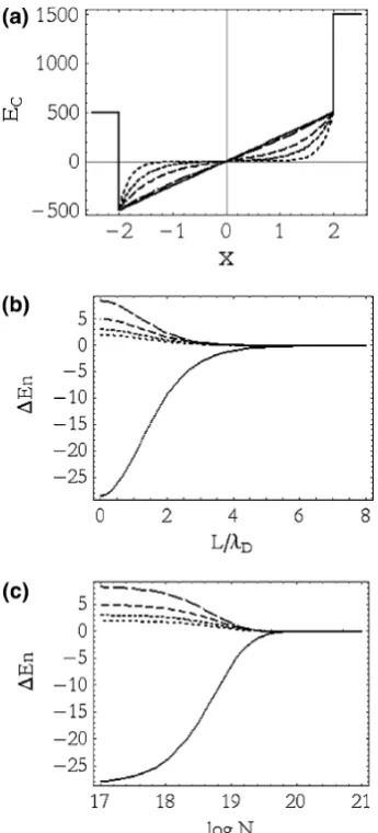
The shift in energy levels relative to the square QW eigen values, obtained from (7), is plotted in Fig.2a versus the ratio jDL:L/kD for the lowest three modes. The
chosen parameters are peak-to-peak sheath potential 2Vo
= 50 meV, QW widthL= 8 nm andme*/me= 0.19 for GaN.
For kD L/2 the polarization field is nearly unshielded,
[image:3.595.84.257.56.437.2]the potential profile nearly linear, and the red-shifting hovers near the maximum value, characterizing the ordin-ary QCSE. Red shifting is however reduced rapidly as the screening range becomes equal or shorter than half the QW width, kDBL/2, becoming completely negligible at
Fig. 2 a Profile of a QW conduction band with a ES-shielded polarization field for characteristic shielding distance (Debye length)
kD=8L,L/2,L/6,L/10,L/20, longer to shorter dash lines.bEnergy correction (meV) versusL/kD, for the lowest five QW modes with
Vo=25 meV and QW width L=8 nm. c Same versus carrier
kD\L/4. Beyond this point the energy levels revert to the
square QW eigen values and the QCSE is completely ‘‘rectified’’. Using the scaling kD¼
ffiffiffiffiffiffiffiffiffiffiffiffiffiffiffiffiffiffiffiffiffiffiffiffiffiffi
4poe2Ne=jT
p
with the valueo ¼8:9 for the GaN dielectric constant recasts
energy shift Fig.2a in terms of the carrier density Ne,
Fig.2b. Complete shielding of the QCSE occurs at Ne
C1020cm-3. This value agrees well quantitatively with similar results obtained in [17], based on the observed decrease in the radiative emission time.
As expected, perturbation theory breaks down when the polarization potential exceeds the unperturbed (square QW) energy eigen valueseVoCE1
(0)
*31 meV. Since the combined inherent and strain-induced polarization fields can reach values up to 5 MeV/cm [18] andVo’LEo=2 up
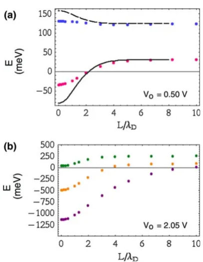
to 2.5 V over a 10 nm QW, numerical solutions of Schrodinger Equation are required for realistic polarization values. For comparison Fig.3 plots the lowest energy levels obtained from numerical solutions (points) and perturbation theory (curves) versus the ratioL/2kD for Vo
= 0.250 V. For unshielded or partially shielded QCSE with kDBL/4 the perturbation theory overestimates the
red-shift by a factor of 2. Good agreement occurs forkD\L/8
when the charged layer thickness is much smaller than the QW thickness, and thus the size of the perturbation, parameterized by R0Ldxsinhðx=kDÞ !kD=L becomes
negligible.
It is useful, for the discussion that follows, to obtain an analytic estimate of the carrier energy eigen values for arbitrary Vo and kD. To that end the eigenfunctions of
Eq. 2 are obtained in terms of an infinite power series expansion a la Frobenius, Appendix 1. The fast conver-gence of the series solutions allows the calculation of the expectation values of the kinetic energy hh2o2x=2mi;
potential energyheU(x)i and the total energy expectation value, yielding
hEni ¼ jCoj 2 h2
2m Kn
k2DeVoWn
" #
; ð8Þ
where Kn, Wn are functions of eVo/jT and the quantum
numbern, andCois the wave function normalization
con-stant. The kinetic energy/1=k2Dincreases with decreasing kD, while the potential (‘‘edge-binding’’) energy is fixed.
ForeVo[5jTthe ratioW1/K1for the fundamental mode is
nearly constant and hovers close to 1/2, Appendix1. The reduction of the red shift with increasing ES shielding and decreasing shielding distancekD, manifested
experimentally as a blue shift relative to the unscreened QCSE, is qualitatively understood as following. For kD\L/2 the sinh(x/kD) potential behaves like an edge-well
inside the square well, instead of a tilted QW floor. If confinement within the edge-well occurs, the lowest energy level must satisfy hE1iB0. As long as the confined
‘‘kinetic energy’’K1h2=2mek 2
Dis less than the edge-binding
energyeVoW1thenE1\0 and the wave function is trapped
at the QW edge. Edge-confinement within a range shorter than the well width,kD\L/2, increases the mode energy
relative to that for a tilted QW bottom and causes blue shift relative to the unshielded QCSE. The blue-shift increases with increasing carrier density, meaning shorter confine-ment lengthkD. Eventually, for large enough density with
kD
ffiffiffiffiffiffiffiffiffiffiffiffiffiffiffiffiffiffiffiffi
meV o=h2
q
; the kinetic energy exceeds the edge-binding energy andhE1i[0, edge confinement ceases, and
the wave function shifts to the center to occupy the full QW width. At the same time most of the well bottom becomes nearly as flat as in a square well, sinceEis excluded from most of the interior. Full ‘‘rectification’’ of the QCSE occurs and the eigen values and eigen modes approach that of a square QW.
Transition from edge-confinement to full QW occupa-tion occurs for either Vo\Vth or kDkth; where
Vthh2=emek 2
Dis the threshold under givenkD, andkth
h= ffiffiffiffiffiffiffiffiffiffiffiffiffieVome
p
the threshold under givenVo. This transition is
shown in Fig.4a and b, plotting the fundamental mode profilesW(x) for various values ofkD/L, for low and high
voltages, respectively Vo= 0.250 V and Vo= 2.05 V. As
[image:4.595.68.272.404.667.2]the screening distance decreases, the center of the wave function moves from the left edge towards the center of the Fig. 3 aNumerical (points) and theoretical energy values (lines) for
the lower two eigen modes versus L/kD for Vo = 0.500 eV. b
Numerical energy values for the lower three eigen modes versusL/kD
well. The transition to full QW occupancy occurs at shorter screening lengthkDfor higherVo(Fig.4b).
Figure5a plots the lower two eigen values versus sheath potential, for given kD=L/8. The fundamental E1
becomes positive at about Vo’Vthh2=emek 2 D: For
Vo\Vththe valueE1increases and tends to the square well
limit as Vo^0. Figure5b shows the fundamental eigen
value E1 versus L/kD for two different voltages Vo. The
eigen values asymptote to the square QW limit at shorter screening distance for the case of higher polarizationVo.
Radiative Emission Probability
The changes in the wave function profiles have a profound influence in thee-htransition probability during radiative emission, proportional to the dipole moment overlap integral
peh ¼
Z
dr3WhðrÞuvðrÞrrWeðrÞucðrÞ ð9Þ
where ucðrÞ; uvðrÞ are the lattice-periodic parts and
WeðrÞ; WhðrÞ the slowly varying envelope functions
obtained from (2). Employing, as usual, the space-scale separation between the rapidly varying, on the lattice-constant scale,uc,uv, and the slowly varying envelopes, valid
for as long asL,kDa, the above is approximated by
peh’
Z L=2
L=2
dxwhðxÞweðxÞ Z Z
dydzeikexxikxhxeikeyxikhyx
Z
C
dr3uvðrÞrrucðrÞ: ð10Þ
Orthogonality among the lattice functionsuc,uv was used
in arriving at (10). The last integral over the unit lattice unit cell volume C is independent of the polarization. For ‘‘vertical transitions’’ with kekh¼kp’0 (given that
kp¼x=c jke;hj) the dependence on the polarization
voltageVoand screening distance kDis carried entirely in
the overlapping between electron-hole envelopes peh¼G
Z L=2
L=2
dxwhðx; Vo; kDÞweðx; Vo; kDÞ ð11Þ
with GRCdr3u
vðrÞrrucðrÞ a constant. Here we will
assume, due to the symmetry in the sinh potential, that
- L/2
-0.2 -0.1
-0.1
1 2 3 4
0.1 -0.2
-1 -1.2 -5 -2.5
0.1 0.5
L/2
- L/2 x L/2
x
λD = 100 L
λD = 100 L
λD = L/2
λD = L/6
λD = L/4
ψ ψ
λD = L/4
λD = L/6
λD = L/10
λD = L/12.5
(a)
(b)
Fig. 4 Normalized wave function profiles (a.u.) for various values
kD/Las marked and for:aVo=0.25 eVbVo=2.05 eV. Transition
from edge-trapping to full QW occupation occurs at shorter kD
[image:5.595.319.527.53.332.2](higher carrier density) for higher polarization voltage
Fig. 5 aEnergy levels for the lower two eigen modes versusVofor
fixedkD=L/8 b Fundamental level versusL/kDfor two polarization voltagesVo=0.250 V andVo=2.05 V, corresponding to
[image:5.595.53.287.59.422.2]Wh(x) =We(L-x). Taking the transition probability for a
flat QW with we;hðx; Vo¼0; kD¼ 1Þ ¼cosðpx=LÞ=
ffiffiffi
L
p
as reference, and since the emission time s/1=p2eh; one has
s1 s1 o
¼
RL=2 L=2dxw
hðx; Vo; kDÞweðx; Vo; kDÞ
h i2
RL=2
L=2dxcosðpx=LÞ 2
=L
h i2
¼
Z L=2
L=2
dxwðxL; Vo; kDÞwðx; Vo; kDÞ
" #2
ð12Þ
The ratioso=sis potted in Fig.6a versusL/kDfor various
peak voltagesVo, using the wave function profiles obtained
from numerical solutions. Characteristic emission times tend to increase with increasing applied polarization volt-age Vo, and decrease with decreasing screening distance
kD. The results of Fig.6a are plotted verusus the
corre-sponding carrier densityNin Fig.6b, for QW width 8 nm. These results reproduce the three order of magnitude emission increase between densities 1019 and 1021, result-ing in complete rectification of the QCSE, that was first obtained using detailed Poisson–Schrodinger simulations in Ref. [17] for a 7 nm QW.
A careful comparison between the energy blue-shifting with increasing density (screening), Fig.7a, and the decrease in recombination time, Fig.7b, shows that the rectification of the QCSE red-shift occurs before the
recovery of the radiative emission time: the energy red-shifting is gradually eliminated first, between densi-ties 1017cm-3and 1019cm-3, though the radiative emission time remains almost constant there. The emission proba-bility is restored, rather abruptly, at higher densities between 1019cm-3 and 1020cm-3. This lagging in restoring the emission probability is explained via edge-carrier trapping, mentioned in the previous discussion. As carrier density increases and the edge-potential rangekDnarrows down, the
increasing edge-confinement of the wave function causes the energy levelE1/h2=2mk2Dto increase. As long as the
‘‘confinement energy’’ h2=2mk2D is smaller than the edge potential deptheVoelectron and hole wave functions remain
edge-localized and no significant change in overlap and in recombination time occurs. The abrupt decrease in the radiative emission time (increase in the radiative emission rate) occurs after h2=2mk2D eVo; since at this point the
wave function moves from edge-confinement to full QW occupancy. Practically this means that the QCSE-related energy red-shift has already been eliminated before the radiative emission time recovers. This behavior agrees with the results in [17].
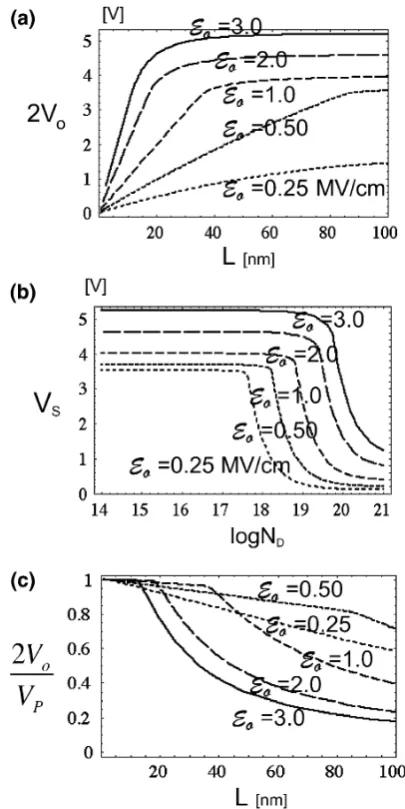
Shielding of the Peak Polarization Voltage
[image:6.595.321.525.53.318.2]It has so far been tacitly assumed that the charged layer peak-voltage Vo is independent of the screening carrier
Fig. 6 aRatio of radiative emission time for a flat QW to that of the ES-shielded QCSE versus screening distanceL/kD, for low and high polarization voltages b same plotted versus corresponding carrier densityNfor an 8 nm QW
[image:6.595.70.271.408.665.2]density Ne,h and the peak-to-peak voltage 2Vo was taken
equal to the ‘‘polarization voltage’’ Vp EoL for an
unscreened QW, Fig.2a. In other words the shielding only modified the potential profile across the QW. However, for given appliedEoandL, the shieldedVodoes depend on the
carrier density, and in factVois reduced belowVpat high
carrier densities. The shielding of the peak voltage is summarized below, based on results from earlier studies [15].
Self-consistent charged layer solutions under Fermi– Dirac thermodynamic equilibrium [15] show that as the QW thicknessLincreases well beyondkDthe peak-to-peak
voltage asymptotes rapidly to a maximum saturation value VsðEo;NÞ:Figure8a plots 2VoversusL for various
polar-ization strength values and shows the saturation 2Vo!
Vs¼constant for L/kD1. Clearly Vs increases with
polarization strengthEo:The dependence ofVson density
is given in Fig.8b. The fact that Vs decreases with
increasing density stems from Gausses law: it takes a given amount of surface charge 4preNodL¼ Eo to screen a
given field. Applying scaling arguments the charge layer thickness isdL ðEo=2Þ=4peNo (half of the electric field
screened at each QW edge) and the sheath voltage eVo4peNodL2=2¼ ðE2o=4Þ=2ð4peNoÞ ¼k2De
2E2 o=8ðjTÞ:
Thus for given polarization Eo the voltage Vs scales
roughly ask2D/1=No when L[2kD.
The screened voltage value is always less or equal to the intrinsic ‘‘polarization voltage’’, 2VoVsVp EoL:
This is shown in Fig.8c, plotting the ratio of the peak-to-peak voltage 2Vo to Vp, versus sheath length, for given
doping densityND = 1018cm-3. For as long as LB 2kD
one has unsaturated behavior 2Vo’Vp/L:Once
satura-tion is reached for L[2kD the peak-to-peak voltage is
pinned at Vs, independent of L. This is because when
L[2kDthe polarization field is screened-out from the QW
interior lengthL-2kDthat yields a negligible contribution
to the voltage difference; Vs comes entirely from two
charged layers of widthkD. Hence, for wide QWs the
peak-to-peak voltage turns out much smaller than the polariza-tion voltage, and the ratio 2Vo/Vpgoes as 1/L. Notice that
the saturation lengthLswhere 2Vodips below Vpdepends
also on the field strength; letting Ls’kD and Vs¼
L2se2E2o=8ðjTÞ ¼Vp¼ EoLs yields Ls¼8jT=Eo;thus
sat-uration occurs at smaller QW thickness with increasingEo.
According to Fig.8c, one may apply unsaturated values 2Vo’Vp for QW thickness L\10 nm and for
Eo3 MV/cm; up to doping densities 1019cm-3. This is
illustrated in Fig.9, plotting the ratio 2Vo/Vpversus doping
density ND for fixed QW L =8 nm and for various
strengthsEo:
For givenL=8 nm, the values 2Voassume their
satu-ration values and the shielded voltage falls significantly belowVpwhen doping densities exceedC1020cm-3. This
Fig. 8 Carrier density effects on the shielded voltage.apeak-to-peak voltage versus QW thickness for doping densityND=1018cm-3and
various polarization strengths, as markedb Saturated peak-to-peak voltage versus doping densityNDfor various polarization strengthsc
ratio of peak voltage to the polarization potential versus QW thickness for doping densityND=1018cm-3
Fig. 9 ratio of peak voltage to the polarization potential versus doping density ND in a QW of thickness L=8 nm, for various
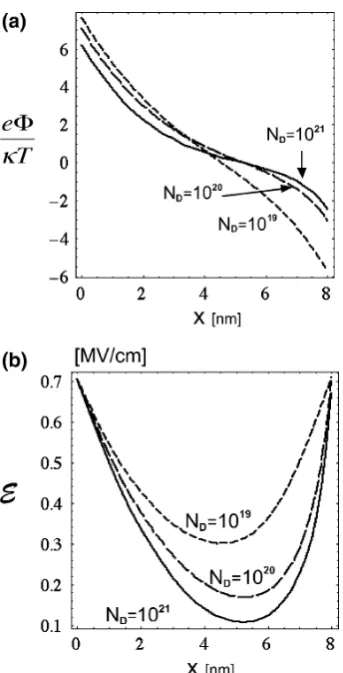
[image:7.595.321.524.56.461.2] [image:7.595.323.526.546.678.2]is illustrated in Fig.10, showing the screened potential profiles, 10a, and electric fields, 10b, for various doping levels ND across an 8-nm QW for Eo¼0:7 MV/cm: The
peak-to-peak voltage decreases well below Vp with
increasingND. In addition, the electron and hole charged
layers become asymmetric:Veacross the negative charged
layer is different thanVhacross the positive charged layer.
In general, reduction of the peak-to-peak voltage, as well as asymmetric electron-hole profiles should be considered for a more accurate description of the ES shielded QCSE. In particular, the drop in Vs\Vp with increasing density
could accelerate the cancellation of the QCSE and the blue shifting of the energy levels. For the relevant to our GaN experiments parameters, however, the red-shifting is all but cancelled out at density 1019cm-3, just before such effects become significant. Thus it appears that energy level blue-shifting caused by the sinh effect in the potential profile cancels to a large degree the QCSE effect, before shielding of the peak amplitude itself becomes important.
Conclusions
A simplified model employing ES-shielded, exponentially-decaying polarization potentials localized at the QW edges, was employed to study the QCSE at high doping densities. Blue shifting of energy levels relative to the unshielded QCSE occurs with increasing carrier density, due to the wave function constriction within scale length kD\L/2.
When the ‘‘edge-localization energy’’h2=mk2Dexceeds the peak-voltage of the charged layer eVo the wave function
center shifts to the middle of the QW and behavior becomes similar to that of a square (unbiased) QW. In addition, at very high doping the shielded peak voltage is reduced well below the original unshielded ‘‘polarization voltage’’ Vp.
Both effects cause gradual elimination of the QCSE red-shifting, an increase in thee-hwave function overlap and a decrease of the radiative emission time. A significant reduction of the peak polarization voltage requires higher carrier densities than most practical situations, and screen-ing effects stem mainly from the interior-screenscreen-ing and the localization of the polarization voltage within QW edge-layers. Our theoretical estimates show that the elimination of the QCSE related red-shift in energy precedes the recovery in the radiative emission time, in quantitative agreement with experimental measurements in [17].
Appendix-1: 1-D Edge-confined Modes—Asymptotic Polynomial Expansions
Section ‘‘QW Eigen Modes with ES-shielded Polar Potential’’ derived a perturbative solution for the edge-confined modes in terms of the square well eigen modes. Another approach, involving an infinite series polynomial expansion, will be given here and used to derive the scaling of the edge-confined expectation values for the kinetic and potential energy. First, forkDL/2 one may approximate
the sinh potential for x\0, U¼ Vosinh½jxj=kD=
sinh½L=2kD;as Voexp½ðjxj L=2Þ=kDþL=2kD=exp½L=
2kD ¼ Voexp½f=kD where f the distance from the
edge fL=2 jxj: The sinh Schrodinger Equation 2 is then approximated by one for an exponential potential
eVoexp½f=kD which has been analyzed elsewhere.1A
dimensionless scaling measuring length in units ofkDand
energy in units ofh2=2mk2Dyields
d
2
df2wn Voe
fw
n¼ enwn; ð13Þ
where n labels the energy quantum number En en: A
[image:8.595.85.257.327.664.2]change of variable w¼ef for f[0 with dw=df¼
Fig. 10 a Self-consistent shielded potential profiles across an
L=8 nm QW for intrinsic polarization fieldEo¼0.7 MV/cm, for various carrier densities as marked.bCorresponding shielded electric field profiles
1 The solutions with
wdw=dwremoves the exponential term and reduces (13) to
w2 d
2
dw2wnþw
d dwwnþ
Vowwnenwn¼0: ð14Þ
The boundary conditions atf¼0;1correspond tow= 1, 0, and are given bywf¼1¼ww¼0¼0:A series expansion
wn ¼wn
X1
l¼0
clwl ð15Þ
inside (14) yields the coefficient recurrence relationclþ1¼
clðVoÞ=ðlþ2nÞ;or ,
cl¼co
ðVoÞl
ð1þ2nÞð2þ2nÞ ðlþ2nÞ¼coðVoÞ
l l!
ðlþ2nÞ!
ð16Þ
where ðlþ2nÞ! ð1þ2nÞð2þ2nÞ ðlþ2nÞ ¼
Cðlþ2nÞ=Cð2nÞ and cn
o is found from the normalization
condition. Substitution into the series solution and application of the boundary conditions at w¼1ðf¼0Þ
yields the eigen values n¼ þ ffiffiffiffien
p
from the roots of the following indicial equation
1þX
1
l¼1
ðVoÞl
l!ðlþ2nÞ!¼0: ð17Þ Switching (15) back to the original variables yields the corresponding eigenfunctions as
wnðfÞ ¼
X1
l¼0
cmleðlþnnÞf=kD
¼X
1
l¼0
coðVoÞl
l!
ðlþ2nnÞ!
eðlþnnÞf=kD ð18Þ
making use of n¼ þ ffiffiffiffien
p
: The leading term goes as exp½ ffiffiffiffien
p
f=kDand gives the asymptotic behavior atjfj kD: For practical purposes is suffices to keep polynomial
terms up to order M equal to twice the integer part ½Vo
inside the infinite sum in (17).
One may now compute expectation values with direct integration of (18). First, orthonormalizationR01dfWW¼
1 yields the normalization constantcofrom
kDjcoj2
X1
l¼0
X1
k¼0
ðVoÞlþk
lþkþ2nn
l!k!
ðlþ2nnÞ!ðkþ2nnÞ!
¼1 ð19Þ
The expectation potential energy heVi ¼ R01dfeVoef=kDWW yieldshVi ¼kDjcoj2eVoW with
Wn¼
X1
l¼0
X1
k¼0
ðVoÞlþk
lþkþ2nnþ1
l!k!
ðlþ2nnÞ!ðkþ2nnÞ!
ð20Þ
and the expectation kinetic energy hKni ¼ ðh2=2mÞ
R1
0 dfW d
df2W yieldshKni ¼kDjcoj
2
ðh2=2mÞKn=k2D
Kn¼
X1
l¼0
X1
k¼0
ðVoÞlþk
ðlþ2nnÞðlþ2nnþ1Þ
lþkþ2nnþ2
l!k! ðlþ2nnÞ!ðkþ2nnÞ!
ð21Þ
Thus the energy expectation valuehEniis
hEni ¼kDjcoj 2 h2
2m Kn
k2D
eVoWn
" #
ð22Þ
where the normalization factor jcoj 2
kD jCoj 2
1 from (19). Thus edge detrapping at about hE1i[0 occurs for
k2D ðh2=2meVoÞ=ðW1=K1Þ:BothKandWdepend onVo
and on the energy eigen value-e1wheree1=n1 2
. The ratio W1/K1 is plotted in Fig.11 versus the peak voltage Vo
(normalized in units ofjT) using the lowest mode energy n =1 inside (20) and (21). Note that forVo[5jTthe ratio
hovers near 1/2 and thus detrapping occurs at kDh= ffiffiffiffiffiffiffiffiffiffiffiffiffimeVo
p
:
Appendix 2: Charged Layer Potential
The self-consistent Poisson’s equation, including the influence of the charged layer (plasma sheath) potential U(x) on the Fermi–Dirac occupation number f in deter-mining the local carrier density is
d2
dx2U¼ qðU½xÞ; ð23Þ
subject to the boundary conditions dU=dxjx¼L=2¼
dU=dxjx¼L=2¼ Eo:This means thatEðxÞ
equals the unshielded value at each QW edge. Above we have normalizedU!eU=jT; x!x=kD andq!q=eNo
whereffiffiffiffiffiffiffiffiffiffiffiffiffiffiffiffiffiffiffiffiffiffiffiffiffiNo is a reference carrier density and kD¼ jT=4pe2N
o
p
[image:9.595.319.526.551.685.2]the corresponding Debye length which includes the dielectric shieldingefrom core (bound) elec-trons. The sum of the electron, hole and charged donor charge densities (N-doping is assumed without loss of
generality) on the right-hand side follows from the equi-librium Fermi–Dirac occupation numbers,
qðxÞ ¼
Z 1
EC
dE GeðEÞ 1þeb½UþEFþ
Z EV
1
dE GeðEÞ 1þeb½UEþF
þND 1
1 1þeb½UþEF
ð24Þ
withEC,EV,Fbeing respectively the conduction, valence,
and Fermi levels, Ge,h(E) the electron (hole) density of
states andND the dopant density (normalized toNo), and
b1=jT: The Fermi levelFis obtained from the condi-tion q[xo|U=0] = 0 at the neutral point U(xo)=0. This
automatically guarantees total charge neutrality over the QW as follows. The pointxowhereq(xo) = 0 is also the
location of the minimum of the screened electric field, since dE=dxjxo¼4pqðxoÞ ¼0 there. Now, from EðL=2Þ
EðxoÞ ¼ ½EðL=2Þ EðxoÞ and Gausses law follows
Rxo
L=2dxqðxÞ ¼
RL=2
xo dxqðxÞandQ-= -Q?. The sheath Eqs. 23 and 24 yield the free carrier dielectric shielding inside a plasma-filled QW capacitor of plate charge r¼ Eo=4punder the nonlinear responseq[U].
Analytic solutions of (23) and (24) in terms of the polarization field strength E exist for certain degenerate ejEFj jT and non-degenerate ejEFj jT limits. The simplest treatment illustrating all the salient features is the undoped (intrinsic semiconductor) limitND= 0. Since
the Fermi level in this case lies close to mid-bandgap and
jFEV;Cj jT; the non-degenerate Maxwellian limit
applies for the carrier statistics. The carrier density is simply given byNe;h¼noe;hexp½eUðxÞ=jTwherenoe;h¼
ni¼ ð1=4Þ 4memej2T2=p2h 4
3=4
exp½EG=2jTis the zero
polarization electron and hole density. Three dimensional density of states is assumed for large enough QW width with small energy spacingDEi’jT:Poisson’s equation is
then simplified to d2
dx2U¼ 2sinh½U: ð25Þ
It has exact analytic solutions, sincex=X(U) is given in terms of elliptic integrals of complex argument, and hence U(x) follows in terms of the elliptic amplitude (Jacobi amðuÞ ¼sin1½snu) function,
Uðx;VL;EoÞ ¼
2
iam iðxL=2Þ
ffiffiffiffi
C
p
;2
C
ð26Þ
whereVL UðL=2Þis the potential drop over half the QW
length L and C1þ E2
o=4coshVL (Different profiles
apply for given applied voltages [19] across the sheaths.) The field and voltage profiles have respectively even/odd symmetry about the middle of the QW, EðxÞ ¼ EðL=2
xÞ;UðxÞ ¼ UðL=2xÞ; reflecting the opposite electron
and hole densities for an undoped material. The opposite polarity electron and hole sheath potentialsVe=-Vh= Vo
are respectively defined by Ve :U(0)-U(L/2) and Vh
:U(L/2) - U(L). The corresponding nominal sheath lengths areLe=Lh= L/2. However, whenLe,hkD, the
field in each sheath is essentially localized within a fewkD
while the rest of the length is almost field-free.
Solutions and shielded voltage profiles for both Max-wellian, Eq. 26, as well as Fermi–Dirac distributions in general, Eqs.23,24, have been given in [15]. Maxwellian profiles are reasonably well fitted with sinh-profiles employed in the present analysis, such as the bottom of the QW Fig.2a. The screened profiles remain essentially similar for Fermi–Dirac distributions in general, as shown in Fig.9a, with one difference: the symmetry between the electron and hole charged-layers is broken,Ve=-Vh. In
addition, F-D statistics yields higher saturation voltages VSunder given parameters. The saturation values shown in
Fig.7 correspond to general F-D solutions. Finally, for sufficiently small potentialseVo=jT ’eEokD=jT 1 any
sheath profiles, including (26), are reduced to exponential profiles [15]UðxÞ ¼Voexpð
ffiffiffi
2
p
xÞ;solutions of the linear differential equation d2
dx2Uþ2U¼0:
References
1. R. Langer, J. Simon, V. Ortiz, N.T. Pelekanos, A. Barski, R. Andr, M. Godlewski, Giant electric fields in unstrained GaN single quantum wells. Appl. Phys. Lett.74, 3827–3829 (1999) 2. W. Franz, Z. Naturforsch.13a, 484 (1958).
3. L.V. Keldysh, The effect of a strong electric field on the optical properties of insulating crystals. Soviet Phys. JETP34, 788–790 (1958)
4. K. Tharmalingam, Optical absorption in the presence of a uni-form field. Phys. Rev.130, 2204–2206 (1963)
5. M. Matsuura, T. Kamizato, Subbands and Excitons in a quantum well in an electric field. Phys. Rev. B33, 8385–8389 (1986) 6. D.E. Aspnes, Electric-field effects on the dielectric constant of
solids. Phys. Rev.153, 972–982 (1967)
7. B.R. Bennet, R.A. Soref, Electrorefraction and electroabsorption in InP, IGaAs, GaSb, InAs and InSb. IEEE JQE23, 2159–2166 (1987)
8. D.A.B. Miller, D.S. Chemla, S. Schmitt-Rink, Relation between electroabsorption in bulk semiconductors and quantum wells: The quantum confined Franz–Keldysh effect. Phys. Rev. B33, 6976– 6982 (1986)
9. H. Shen, F.H. Pollack, Generalized Franz–Keldysh theory of electroabsorption. Phys. Rev. B42, 7097–7102 (1990)
10. R.J. Elliot, Intensity of optical absoprtion by excitons. Phys. Rev. 108, 1384–1389 (1957)
11. M. Shinada, S. Sugano, Interband optical transitions in extremely anisotropic semiconductors I: bound and unbound exciton tran-sitions. J. Phys. Soc. Jpn.21, 1936–1946 (1966)
13. S.L. Chuang, S. Schmitt-Rink, D.A.B. Miller, D.S. Chemla. Exciton Green’s function approach to optical absorption in a QW with an applied electric field. Phys. Rev. B43, 1500–1509 (1991) 14. C.Y.P. Chao, S.L. Chuang, Analytical and numerical solutions for a two-dimensional exciton in momentum space. Phys. Rev. B43, 6530–6543 (1991)
15. S. Riyopoulos, T.D. Moustakas, J.S. Cabalu, Plasma nanosheath formation with carrier accumulation and enhanced localized spontaneous emission at quantum wedges in textured GaN, sub-mitted to Phys. Rev. B14, 053501 (2007)
16. F. Della Sala, A. Di Carlo, F. Bernardini, V. Fiorentini, R. Scholz, J.-M. Jancu, Free-carrier screening of polarization fields in wurtzite GaN/InGaN laser structures. Appl. Phys. Lett.74, 2002 (1999) 17. A. Thamm, O. Brandt, J. Ringling, A. Trampert, K.H. Ploog, O.
Mayrock, H.-J.Wu¨nsche, F. Hennberger, Optical properties of heavily doped GaN/(Al,Ga)N multiple QWs grown on 6H-SiC(0001) by reactive molecular-beam epitaxy. Phys. Rev.61, 16025 (2000)