Article
On the Effect of Selective Laser Melting process
parameters on the microstructure and mechanical
properties of Al Alloys
Ahmed H. Maamoun *1, Yi F. Xue1), Mohamed A. Elbestawi 1), Stephen C. Veldhuis1)
1 McMaster University, Department of Mechanical Engineering,1280 Main Street West Hamilton, ON, Canada, L8S 4L7
* Correspondence: [email protected]; [email protected]
Abstract: Additive manufacturing (AM) offers customization of microstructure and mechanical properties of fabricated components according to the material selected, and process parameters applied. Selective laser melting (SLM) is the commonly used technique for processing high strength aluminum alloys. Selection of SLM process parameters could control the microstructure of parts and their mechanical properties. However, the process parameters limit and defects obtained inside the as-built parts present obstacles to customized part production. This study investigates the influence of SLM process parameters on the quality of as-built Al6061 and AlSi10Mg parts according to the mutual connection between the microstructure characteristics and mechanical properties. The microstructure of both materials was characterized for different parts processed over a wide range of SLM process parameters. The optimized SLM parameters were investigated to eliminate the internal microstructure defects. The behaviour of mechanical properties of parts was presented through regression models generated from the design of experiment (DOE) analysis for the results of hardness, ultimate tensile strength, and yield strength. A comparison between the results obtained and that reported in the literature is presented to illustrate the influence of process parameters, build environment, and powder characteristics on the quality of parts produced. The results obtained from this study could help to customize the part’s quality by satisfying their design requirements in addition to reducing the as-built defects which in turn reduce the amount of the post-processing needed.
Keywords: additive manufacturing; selective laser melting; AlSi10Mg; Al6061; SLM process parameters; quality of the as-built parts
1. Introduction
Additive manufacturing (AM) is considered one of the leading sectors of the upcoming industrial revolution “Industry 4.0” [1]. AM of metals using selective laser melting (SLM), promises significant development of a variety of critical applications in different industrial fields [2]. AM of Al alloys could produce high-performance lightweight components with relatively high material quality, mechanical properties, and design flexibility. Selection of the SLM process parameters plays an essential role in controlling the material and mechanical properties of products customized according to their function and design requirements. The effect of the SLM process parameters on the quality of Al alloys was previously presented in some studies [3–9]. Prashanth et al. [12] reported that the selected strategy of hatch spacing and contour parameters could significantly affect the microstructure and mechanical properties of the AlSi12 parts fabricated using SLM. Their results showed that applying the contour parameters is negatively affect ductility of parts due to the residual stresses along the surface. However, the effect of the SLM parameters on the microstructure of the AlSi12 parts was not reported in this study. Biffi et al. [8] studied the influence of the SLM energy density on the mechanical properties of the AlSi10Mg samples. However, the effect of each process
parameter was not studied to detect the leading parameter affects the microstructure and mechanical properties. Li et al. [10] reported that the high cooling rate during the SLM process of AlSi10Mg results in ultrafine-grained microstructure and thus leads to superior mechanical properties as compared to casted material of the same alloy. The microstructure characteristic could be affected by the applied cooling rate according to the selected SLM parameters. Akram et al. simulated a model of grain structure evolution in the multi-layer deposition during the SLM process [11]. Their results illustrated the change in grain size and orientation according to the process parameters applied.
In SLM of Al alloys, the chemical composition of the Al alloys could result in variation between their microstructure and mechanical properties, due to the difference in some elements such as Si and Mg. However, SLM of some Al alloys, such as Al6061, results in solidification and liquation cracking due to the material’s relatively higher coefficient of thermal expansion (CTE) [3]. This is why AlSi10Mg is the most commonly used Al alloy for the SLM process due to its lower CTE compared to the Al6061 alloy [12]. The Si content may also play a significant role in microstructure evolution and the elimination of hot cracks. Uddin et al. [13] reported that preheating the build plate at 500˚C using specific process parameters resulted in crack-free parts. However, the mechanical properties of the fabricated components are adversely affected as compared to as-built parts produced without preheating the build platform. Martin et al. [14] studied the effect of adding nanoparticles of some additives to Al6061 and Al7075 alloy powder. Their results showed that the additives added could control the solidification process, and reduces the crack formation inside the as-built parts. However, lower mechanical properties were obtained as compared to the as-built components of the original alloy due to the spherical pores formation. Moreover, the effect of the SLM process parameters for Al6061 alloy was not reported in the literature to investigate the ability to control the hot-crack formation.
Fulcher et al. [12] reported that the SLM process map should be regularly updated for each material as technical capabilities develop. This could help to optimize the SLM process parameters and customize the characteristics of the as-built parts. Consequently, the microstructure and mechanical properties of the additively manufactured parts can be tailored according to their design requirements. In general, the literature studies show the importance to update the SLM process map according to the capabilities of the upgraded machines. This might help to detect the leading parameter affecting each characteristic to achieve the desired quality of the parts fabricated. However, the laser power of SLM was limited to 200 W which is a relatively low figure compared to the currently used laser power which can reach 400 W for the majority of existed machines. Therefore, due to the widespread use of Al6061 in aerospace and automotive fields, a study is recommended of the influence of SLM process parameters on this material. This also might reduce the amount of post-processing applied to heal the as-built part defects.
The current study focuses on the effect of SLM process parameters on microstructure and mechanical properties of both AlSi10Mg and Al6061 as-built parts. This work completes the comprehensive study presented by Maamoun et al. [15] to develop a full process map of different Al alloys fabricated with SLM. Microstructure characterization is performed to investigate the evolution of as-built microstructure along with changing the SLM process parameters. An optimum process parameters range is investigated to reduce the microstructure defects and hot-cracks formation. The behaviour of mechanical properties is studied for both materials. A regression model is created based on the design of experiment (DOE) analysis for each mechanical property along the applied range of SLM process parameters. The regression model trend for each property of the as-built parts is validated according to experimental results and additionally verified with microstructure analysis. A comparison between the obtained results from the current study as compared to literature is conducted to illustrate the effect of powder characteristics, build environment, and process parameters on the properties of parts fabricated. This study presents a process map of the influence of SLM process parameters of AlSi10Mg and Al6061 as-built parts, and this could offer the following:
1- Customization of parts fabricated according to their function and design requirements. 2- Reduction or elimination of the microstructure defects by investigating the optimum range
2. Experimental procedure
In the current study, the samples were produced using the SLM process parameters listed in Table 1, and Table 2. The methodology of the DOE is the same as reported by Maamoun et al. [15]. The technique of one factor at a time (OFAT) is applied for AlSi10Mg parts, and the response surface method is used for Al6061 parts. The correlation coefficient (R2) is used to indicate how the regression
models fit with the measured data, this factor was added to each mechanical property characteristic map for each material. The build plate was preheated to 200 ˚C, before building started under an argon medium. So, AlSi10Mg_200C and Al6061_200C also referred to the as-built AlSi10Mg and Al6061 samples respectively. Powder characteristics, microstructure analysis and the measurement of mechanical properties were performed with the following methods.
Table 1. The SLM process parameters applied for producing the AlSi10Mg_200C samples.
Sample# P (W) Vs (mm/s) Dh (mm) Ed
(J/mm3)
AS1 370 1000 0.19 65
AS2 370 1300 0.15 63.2
AS3 370 1300 0.19 50
AS4 350 1300 0.19 47.2
AS5 370 1500 0.19 43.3
AS6 300 1300 0.19 40.5
AS7 370 1300 0.25 38
AS8 200 1300 0.19 27
Table 2. The SLM process parameters used for building the Al6061_200C samples.
Sample# P (W) Vs (mm/s) Dh (mm) Ed
(J/mm3) Sample#
P (W) Vs (mm/s) Dh (mm) Ed
(J/mm3)
1A 370 1000 0.1 123.3 11A 370 800 0.15 102.8
2A 300 1000 0.1 100 12A 350 800 0.15 97.2
3A 370 1300 0.1 95 13A 370 800 0.19 81.1
4A 300 1300 0.1 76.9 14A 350 800 0.19 76.8
5A 370 1000 0.19 65 15A 370 1300 0.15 63.2
6A 300 1000 0.19 52.6 16A 350 1300 0.15 59.8
7A 370 1300 0.19 50 17A 370 1300 0.19 50
8A 300 1300 0.19 40.5 18A 350 1300 0.19 47.2
2.1. Powder characteristics
ASTM F3049-14 was used to examine the fresh powder of AlSi10Mg and Al6061 after sieving using a 75 µm mesh. The full powder characterization of the same powders used in this study was reported by Maamoun et al. [15,16]. Particle size distribution test showed a particle size ranges from 12 to 120 µm for Al6061 and from 12 to 110 µm for AlSi10Mg. Powder morphology of a spherical particle shape was detected with the existence of some elongated particles that might affect the flowability. Both powders have a positively skewed profile which could result in a higher density and better surface roughness as compared to Gaussian and negatively skewed powder distribution [17].
2.2. Microstructure characterization
samples’ phase analysis. The XRD phase pattern was obtained for each sample along different orientations of the AlSi10Mg and Al6061 samples.
2.3. Mechanical properties measurements
The microhardness measurement was performed according to ASTM E384-17 using an automatic Clemex CMT tester. The average values of the samples’ microhardness were obtained along the building direction (Z-direction), and along the plane parallel to the deposited layers (XY-plane). Each recorded value was an average of 5-10 indentations along the tested area of a 200 gf load applied over a 10 s dwell time. The residual stress was measured by an XRD instrument using a Vantec500 area detector, and the results were analyzed using LEPTOS software. The tensile rod samples were designed and fabricated according to the geometry and dimension included in ASTM E8/E8M – 16a. The tensile test was performed according to ASTM E8 standard procedures using an MTS Criterion 43 universal test system which applies a load capacity up to 50 kN.
3. Results and discussion
3.1. Microstructure
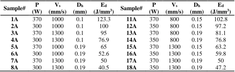
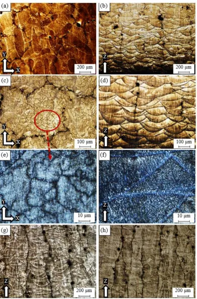
The optical microscope analysis was performed using the as-built etched samples of AlSi10Mg and Al6061. Figure 1 shows the microstructure defects and observations along the building direction (Z-direction) of AlSi10Mg samples fabricated at different SLM process parameters. Figure 1(a) illustrates that process-induced porosity or keyhole pores of 100-250 µm size and irregular shapes are formed inside the AS8 sample fabricated at a low energy density of 27 J/mm3. This results from a
lack of fusion due to insufficient powder delivery to the melted layer. Unmelted powder may be visible around these keyhole pores [19]. Figure 1 (a) also shows that the melt pool solidified with an elliptically shaped profile and these melt pool shapes overlap in a specific arrangement according to the value of hatch spacing used. This shape is related to the Gaussian distribution of laser beam power [18]. Figure 1(b) shows a magnified view of the melt pool shape; a fine grain structure is observed inside, while a coarse grain is formed along its borders due to the gradient change of the solidification rate. Figure 1(c) shows the microstructure of the AS7 sample fabricated at an energy density of 38 J/mm3. The keyhole pore density and size are decreased due to a higher energy density. The melt
pool shape geometry of the AS7 sample is enlarged compared to the AS8 sample due to a diminishing solidification rate together with an energy density increase. In the AS3 sample produced at a 50 J/mm3
energy density, the keyhole pores almost disappeared as shown in Figure 1(d). A coarser grain structure is also present inside and along the borders of the melt pool shape as illustrated in Figure 1(f). At a higher rate of energy density of 65 J/mm3 applied to the AS1 sample, melt pool borders
Figure 1. Microstructure of the as-built AlSi10Mg_200C samples processed under different SLM process parameters; a, c) AS8, b) AS7, d, f) AS3, and e, g, h) AS1.
(
1
)
𝐸
𝑑=
PV𝑠∗𝐷ℎ∗T𝑙
Where Ed represents energy density in J/mm3, P is the laser beam power (W), Vs is the laser scan
speed (mm/s), Dh is the hatch spacing between scan passes, Tl is the deposited layer thickness, which
borders observed inside the AS1 sample might be related to the reduction of the scan speed and hatch spacing parameters.
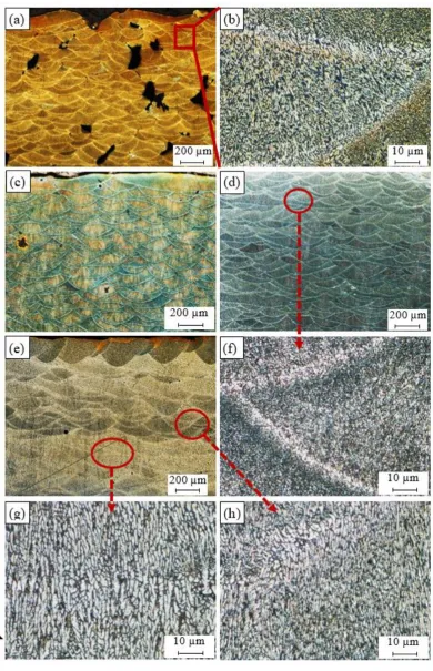
SEM observations in Figure 2 and Figure 3 show the change in the developed microstructure and the evolution of the Al matrix grain size of the as-built AlSi10Mg samples produced at different energy densities and SLM process parameters. Figure 2 displays the microstructure along the Z-direction of the AlSi10Mg samples. In general, the development mechanism of the as-built AlSi10Mg microstructure depends on the mechanism of particle accumulated structure (PAS) formation [21]. The PAS mechanism shows that during the high cooling rate of 106-108 ˚C/s, Si is ejected out of the solidifying Al matrix to form a fibrous Si network around the Al matrix grain borders. At a lower energy density of 27 J/mm3, the microstructure shows an ultra-fine elongated grain structure with an inhomogeneous size distribution of Al matrix grains surrounded by a fibrous Si network. The Al matrix grain size ranges from 0.2 to 2 µm, where the finer grain structure formed inside the melt pool shape and larger grains located around its borders as displayed in Figure 2(a). The increase of energy density to 50 J/mm3 results in the same microstructure formation with a coarser inhomogeneous microstructure and grain size ranging from 500 nm to 3 µm as illustrated in Figure 2(b). Figure 2 (c, d) shows that when the AS1 sample is produced at a higher energy density of 65 J/mm3, an equiaxed larger grain structure is present with Al matrix grain size varying between 3-4 µm. A more homogeneous microstructure is also obtained compared to the samples produced at a lower energy density. The final top layers in Figure 2 (c) have a finer microstructure compared to the vicinity of the middle of the part in Figure 2(d). This is attributed to the thermal gradient difference between these areas during the building of the layers, which affects the solidification rate.
Figure 3. The SEM observations of the as-built AlSi10Mg microstructure along the XY plane; a) AS8, b) AS3, and c) AS1.
The as-built AlSi10Mg samples along the XY plane had an equiaxed grain microstructure as can be seen in Figure 3. The microstructure is inhomogeneous due to the existence of coarser grains along the border of the melt pool profile compared to the microstructure inside. This confirms the PAS formation mechanism of the microstructure development along the XY plane as well as the Z-direction [3,21]. Figure 3 (a) shows the microstructure of the AS8 sample, where an inhomogeneous grain distribution of 0.15-1 µm size can be seen within the fine and coarser Al matrix grain zone. The grain size slightly increased along with energy density. Figure 3 (b) presents the microstructure of the AS3 sample with a grain size ranging from 0.3 to 2 µm. The microstructure evolution of the higher energy density of 65 J/mm3 applied to the AS1 samples has almost the same Al matrix grain structure
value as illustrated in Figure 3(c). Application of energy densities higher than 50J/mm3 caused no
observed evolution of the Al Matrix grain size might be related to the reduction of solidification rate along with increasing the energy density [24].
The XRD phase pattern presented in Figure 4 and Figure 5 shows a comparison of the Al and Si peak characteristics of different AlSi10Mg samples. The Al and Si peak is identified using the Joint Committee on Powder Diffraction Standards (JCPDS) patterns of 01-089-2837, 01-089-5012, respectively. A small peak of Mg2Si is detected according to the JCPDS pattern of 00-001-1192, and
the low intensity of this peak is related to the existence of nano-size Mg2Si precipitates of 20-40 nm
that are hardly detectable with XRD [18,23]. The difference in Al and Si peak width between the samples indicates crystal size change under different SLM process parameters. This can be inferred from Scherrer’s equation, where peak broadening varies inversely with crystallite size [25]. According to the phase pattern obtained in Figure 4, the grain size significantly increased along the Z-direction as energy density increase to 50 J/mm3 before becoming stable at a specific value, which
agrees with microstructure observations in Figure 2. The XRD phase pattern in Figure 5 illustrates the peak broadening comparison along the XY plane, where a slight difference of the crystal size is observed between the samples fabricated at different SLM parameters. This corresponds to the SEM observations in Figure 3. By comparing the peak broadening of the same sample along the Z-direction and the XY plane, a significant difference can be seen in peak broadening and intensity. This difference might result from the change in the crystal shape and size, and microstrain [25,26]. The microstructure is inhomogeneous along different orientations. For more accurate values, an FWHM analysis was performed according to the phase pattern in Table 3. The results showed a broadened peak of Al and Si in the AS8 sample at the lower energy density, with FWHM values of 0.2111 and 0.5935 degrees respectively. This confirms the finer microstructure observed at the lower rates of energy densities in Figure 2. The significant difference of Al and Si peak broadening in the AS8 sample along the XY plane and Z-direction also confirms the microstructure inhomogeneity at the low energy of 27 J/mm3. There is no significant difference between the FWHM values detected along
the top and side orientations of the AS1 sample produced at a higher energy density of 65J/mm3. A
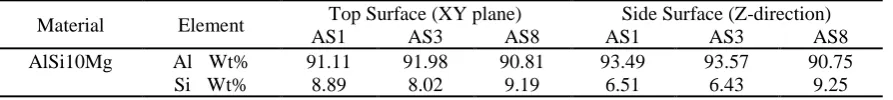
homogeneous equiaxed grain structure is present along the XY plane and Z-direction of the AS1 sample which indicates an improvement of the microstructure homogeneity at the higher energy densities. A Rietveld analysis was performed to detect the relative weight percentage of Al and Si according to the XRD phase pattern measured along the top and side surfaces of the AlSi10Mg samples. The results listed in Table 4 indicate that Si becomes more soluble inside the Al matrix along the XY plane as energy density gets higher. The percentage of Si solubility inside the Al matrix is higher along the Z-direction compared to that in the XY plane for AS1 and AS3 samples after an energy density of 27 and 50 J/mm3 is respectively applied. In addition, the highest percentage of Si
precipitates is obtained at the AS8 sample produced at the higher energy density of 65 J/mm3. These
results validate the thickness increase of the Si network at higher energy densities in Figure 2 and Figure 3. It is worthwhile to note that Rietveld analysis was used to get the indication of the Si solubility change inside the Al matrix along the SLM process parameters applied where the small amount of Mg2Si existed can be neglected in this case [18].
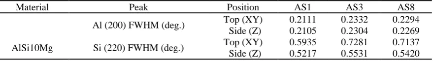
Table 3. The average FWHM of Al and Si peaks according to the XRD phase pattern of the as-built AlSi10Mg samples.
Material Peak Position AS1 AS3 AS8
AlSi10Mg
Al (200) FWHM (deg.) Top (XY) 0.2111 0.2332 0.2294
Side (Z) 0.2105 0.2304 0.2269
Si (220) FWHM (deg.) Top (XY) 0.5935 0.7281 0.7137
Figure 4. XRD phase pattern measured on the side surface (along the Z-direction) of different as-built AlSi10Mg samples.
Figure 5. XRD phase pattern measured on the top surface (along the XY plane) of different as-built AlSi10Mg samples.
Table 4. Rietveld analysis throughout the top and side surfaces of the as-built AlSi10Mg samples.
Material Element Top Surface (XY plane) Side Surface (Z-direction)
AS1 AS3 AS8 AS1 AS3 AS8
AlSi10Mg Al Wt% 91.11 91.98 90.81 93.49 93.57 90.75
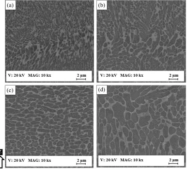
Figure 6. Microstructure of the as-built Al6061 samples processed under different SLM process parameters; a,c,e) 6A along the Z-direction, b,d,f) 6A along the XY plane, g) 14A, and h) 15A.
shape within an average size of 200 µm along the Z-direction and propagate through the middle zone of some solidified melt pool shape as shown in Figure 6 (b, d). A pore of 10-20 µm is also noticed amongst these cracks. The micro-crack formation is caused by high CTE of the Al6061, which in turn, resulted in significant shrinkage due to the rapid melting and solidification rates of the SLM process [12]. A fine grain structure persists along both XY-plane and Z-direction as shown in Figure 6 (e, f). Coarse grains are present around the melt pool profile, which substantiates the thermal gradient inside each melt pool during the solidification process. It is worthwhile to note that no large keyhole pores are observed inside the 6A sample microstructure fabricated with an energy density of 52.6 J/mm3. The evolution of crack formation behaves differently along the Z-direction, corresponding to
the applied energy density and SLM process parameters as shown in Figure 6 (b, g, h). Observations indicate an increase of the crack size and distribution density under higher levels of energy densities as illustrated in Figure 6 (g). Large hydrogen spherical pores were seen forming along the longitudinal micro-cracks as energy density increased. By comparing the microstructure in Figure 6 (b, h), it can be concluded that a higher laser power and lower scan speed significantly increases the length of the cracks and their distribution density due to the imbalance between the higher melting and lower solidification rates.
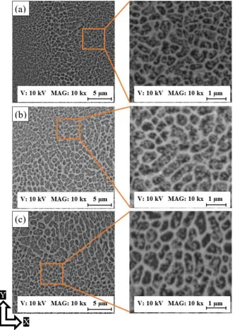
The as-built Al6061 microstructure in Figure 7 shows the precipitation of nano-size Si particles around the Al matrix grains, which confirms the PAS formation mechanism where the Si particles solidified around the Al matrix [21]. However, the same fibrous Si network is not present in the AlSi10Mg, due to Si content in the Al6061 alloy being insufficient to develop this fibrous network. A fine microstructure with an elongated grain form is observed along the Z-direction with a size of 3-5 µm as shown in Figure 7 (a). Along the XY plane, an equiaxed grain structure is present, with an average grain size of (2-4 µm), Figure 7 (b). The difference in the grain structure between these orientations reveals a microstructure inhomogeneity which could result in anisotropic structure properties.
Figure 7. Microstructure grains of the as-built Al6061 sample at a higher magnification.
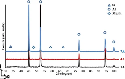
The XRD phase pattern in Figure 8 shows Al and Si peak up on the top surface of the as-built Al6061 samples in the XY plane. Figure 9 illustrates the phase pattern up on the side surface along the Z-direction. The Al peak is identified according to the JCPDS pattern of 01-089-2837. According to the JCPDS patterns of 01-089-5012, a Si peak was hardly distinguishable due to the precipitation of the nano-size Si particles inside the as-built microstructure as displayed in Figure 7. A low-intensity peak of Mg2Si is also detected according to the JCPDS pattern of 00-001-1192 as indicated in Figure 8
and Figure 9. The change of Al peak broadening along the XY plane and Z-direction indicates Al crystal size change according to the specified SLM process parameters. This change is closely investigated according to FWHM analysis listed in Table 5. A wider Al peak is obtained at a low energy density of 50 J/mm3, which confirms the growth of the grain size as energy density increases.
density of 123.3 J/mm3, revealing a coarser grain structure at higher energy densities. There was no
significant difference between the FWHM values of the top and side surfaces. Al6061 microstructure is more homogeneous along the applied range of the selected parameters as compared to the considerable microstructure inhomogeneity inside AlSi10Mg samples. It is worthwhile to note that the Al6061 alloy could be processed at higher energy density values than the AlSi10Mg alloy due to the higher reflectivity of Al6061 which decreases the percentage of absorbed energy. However, SLM process parameters need to be optimized to reduce the formation of micro-cracks and the spherical hydrogen pores.
Figure 8. XRD phase pattern measured on the side surface (along the Z-direction) of different as-built Al6061 samples.
Table 5. The average FWHM of Al (200) peak of the as-built Al6061 samples.
Material Peak Position 1A 4A 7A
Al6061 Al (200) FWHM (deg.)
Top (XY) 0.1874 0.2086 0.2045
Side (Z) 0.1838 0.2042 0.2029
3.2. Mechanical properties
The effect of SLM process parameters on the mechanical properties of the as-built AlSi10Mg and Al6061 parts is investigated according to the regression models developed from experimental results. In the following section, DOE analysis will illustrate microhardness and tensile behaviour according to the selected SLM process parameters.
3.2.1. Microhardness
Figure 10 displays the microhardness of the as-built AlSi10Mg parts along the Z-direction within the range of SLM process parameters. The microhardness ranges between 86 and 103 HV, and the maximum value is obtained at 27 J/mm3 due to smaller grain size as presented in Figure 2(b).
However, a significant amount of keyhole pores are observed at this energy density of the AS8 sample, which underscores the need for SLM process optimization. The results show that microhardness values linearly decrease as laser power and energy density grow as illustrated in Figure 2(a, b). A higher hatch spacing and scan speed improve sample microhardness in Figure 10(c, d). Low values of sample microhardness at low scan speeds result from high solidification rates and low hatch spacing due to decreasing overlap between the scanned passes [3,24]. The microhardness profile of AlSi10Mg samples shows a good agreement with microstructure observations and the crystal size change of SLM process parameters.
As illustrated in Figure 11, microhardness along the XY plane is relatively higher than in the Z-direction, demonstrating the inhomogeneity of the as-built microstructure. The microhardness is 115 to 118 HV along the range of the SLM parameters, which confirms better homogeneity along the XY direction, Figure 3. This trend agrees with literature studies [18,20,22]. The reduction in laser power and greater hatch spacing improves microhardness along the XY plane as shown in Figure 11(a, c). Although the low laser power rates show higher microhardness values, control of SLM process parameters should aim to produce denser parts by reducing porosity. According to Figure 10 and Figure 11, microhardness values correspond to the DOE analysis regression model along both the XY plane and Z-direction.
Figure 11. Microhardness of the as-built AlSi10Mg samples along the XY plane vs. a) Laser power (W), b) Energy density (J/mm3), c) Hatch spacing (mm), and d) Scan speed (mm/s).
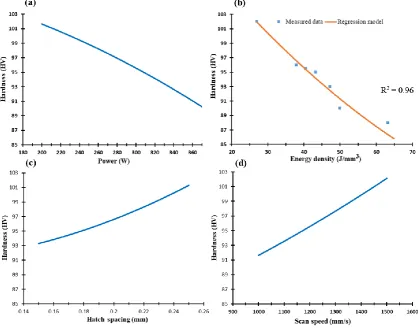
Figure 12 and Figure 13 display the microhardness profile of selected SLM process parameters of the Al6061 parts along the Z-direction and XY plane respectively. The map in Figure 12 shows a gradual decrease of microhardness values along the Z-direction from 85 to 72 HV at an energy density range of 40.5 to 97.2 J/mm3. A slight increase was observed at higher energy densities up to 123 J/mm3
Figure 12. Microhardness of the as-built Al6061 samples along the Z- direction vs. a) Laser power (W), b) Energy density (J/mm3), c) Hatch Spacing (mm), and d) Scan speed (mm/s).
Figure 13 shows microhardness of the Al6061 samples along the XY plane that varies significantly between 62 to 77 HV according to the SLM process parameters. This could be related to the change in micro-crack size as illustrated in Figure 6. Figure 13(a, b) shows microhardness decrease along with laser power and energy density increase due to increasing the solidification rate and thus results in a more coarser grain structure [20]. Figure 13(c, d) illustrates microhardness increase along with increasing scan speed and reducing laser power, and thus indicates that energy density is the leading parameter affects this property. In contrast with AlSi10Mg samples, hatch spacing significantly affects the microhardness of Al6061. Microhardness gradually decreases with the increase of energy density due to the gradient in microstructure characteristics. This is in agreement with the trend reported literature studies [11,20].
Figure 13. Microhardness of the as-built Al6061 samples along the XY plane vs. a) Laser power (W), b) Energy density (J/mm3), c) Hatch Spacing (mm), and d) Scan speed (mm/s).
3.2.2. Tensile properties
The ultimate tensile strength (UTS) of the AlSi10Mg was measured to generate the regression model plots for both as-built and machined tensile samples as presented in Figure 14. The as-built and machined samples possessed the same tensile profile as the samples produced under SLM process parameters. However, the machined samples had higher UTS values of up to 450 MPa compared to those of the as-built samples (400 MPa). This 20 to 50 MPa difference in UTS values indicates the effect of surface roughness on mechanical properties. However, UTS values of the as-built parts could demonstrate the impact of SLM parameters on tensile properties, taking into consideration the surface roughness of each sample. Figure 14 also shows a good agreement between the experimental measurements and the regression model generated from the DOE analysis as illustrated in Figure 14(b). Also, laser power has a more significant effect on UTS sample properties than changes in hatch spacing and scan speed, Figure 14(a, c, d). The optimum UTS value is obtained in the AS3 sample at an energy density of 50 J/mm3. This agrees with the microstructure observation,
which showed minimum defects of the as-built AlSi10Mg sample at these parameters. It is worthwhile to note that better surface roughness of the as-built AlSi10Mg was obtained at higher energy density that 50 J/mm3 [15]. However, the current results indicate that applying an energy
density of 50 J/mm3 is the optimum condition for processing AlSi10Mg alloy using scan speed of 1300
Figure 14. Ultimate tensile strength of the as-built AlSi10Mg samples along the building direction vs. a) Laser power (W), b) Energy density (J/mm3), c) Hatch Spacing (mm), and d) Scan speed (mm/s).
Figure 15 illustrates yield strength versus the scan speed, laser power, hatch spacing, and the energy density for the as-built AlSi10Mg samples. Results indicate a decrease of yield strength within a range of 240 to190 MPa at increasing energy densities as presented in Figure 15(b). A slight difference of 30-50 MPa in yield strength was observed at the range of SLM process parameters, Figure 15(a, b, c, d). This indicates that a change in SLM process parameters has a greater impact on UTS values than the yield strength. From the results illustrated in Figure 14 and Figure 15, UTS and yield strength trends of the s-built AlSi10Mg parts significantly reflect the microstructure observations in section 3.1. An increase of energy density creates a coarser microstructure with lower hardness and tensile values. This trend in agreement with that reported by Ding et al. [29]. Moreover, some results obtained in the current study showed superior values of mechanical properties than that reported in the literature [29–32].
As illustrated in Figure 16 (a, b, c, d), the UTS values of the as-built Al6061 samples were investigated at a range of 150 to 184 MPa. The results indicate a significant reduction in UTS of the Al6061 samples compared to that of AlSi10Mg. This could result from the lower percentage of Si content inside the Al6061 alloy and micro-cracks inside its as-built samples. As energy density increases, UTS values gradually decrease. Figure 16(b) shows that a maximum UTS of 184 MPa was obtained in the 18A sample using the higher scan speed (1300 mm/s), hatch spacing (0.19 mm), and energy density of 47.2 J/mm3. A significant decrease in the UTS values was observed at the lower scan
speed of 800 mm/s and smaller hatch spacing of 0.1 mm, Figure 16(a, c, d). This decrease in the UTS values might result from the microstructure defects at low rates of scan speed and hatch spacing, such as keyhole pores or areas of unmelted powder.
Figure 16. Ultimate tensile strength of the as-built Al6061 samples along the building direction vs. a) Laser power (W), b) Energy density (J/mm3), c) Hatch Spacing (mm), and d) Scan speed (mm/s).
mechanical properties behaviour shows a good agreement with that reported in some previous studies [12,13,33], in addition to detecting the values of SLM parameters that results in a higher values than reported in these studies. It is worthwhile to note that the UTS and yield strength values of the as-built Al6061 samples hardly differ, which indicates the lower ductility of these parts compared to the as-built AlSi10Mg samples.
Figure 17. Yield strength of the as-built Al6061 samples vs. a) Laser power (W), b) Energy density (J/mm3), c) Hatch Spacing (mm), and d) Scan speed (mm/s).
Figure 18. The stress strain diagram for the as-built samples: a) AlSi10Mg; and b) Al6061 samples.
Table 6 summarizes the mechanical property values of the AlSi10Mg and Al6061 samples in the current study, compared to literature. According to values listed in Table 6, the following insights can be drawn:
1. Mechanical properties and Al matrix grain size are illustrated for the as-built AlSi10Mg_200C samples in the current study. Although the lower rate of energy density created a fine microstructure, mechanical properties were inferior due to the internal defects inside the areas caused by lack of fusion.
2. The microhardness reported in a previous study by the authors [18], using the same preheating technique, shows higher values than those reported in this study. This indicates the effect of powder morphology and its particle size distribution. It can be concluded that a wide range of particle size distribution with a spherical shape resulted in high microhardness values. 3. The mechanical properties of the AlSi10Mg_200C samples have relatively lower values than
those of samples produced by build plate preheating [34–38]. However, residual stresses are significantly lower due to the preheating technique [4,18].
4. Superior mechanical properties of the AlSi10Mg_200C samples are detected compared to parts produced with a conventional or the high-pressure die cast (HPDC) material of the same alloy [28,39].
5. As-built Al6061_200C parts had better mechanical properties than Al6061_500C. However, no cracks were observed inside the Al6061_500C as reported by Uddin et al. [33], but the mechanical properties of the part were significantly decreased.
Table 6. A summary of mechanical properties microstructure grain size of the AlSi10Mg and Al6061 parts processed though SLM and the conventional techniques under different conditions.
4. Summary and conclusions
The current study focused on the influence of SLM process parameters on the microstructure and mechanical properties of the as-built AlSi10Mg and Al6061 parts [41]. The mechanical behaviour of these parts along the range of selected SLM parameters was investigated using DOE regression models. The main results are summarized as follows:
1. The microstructure of the AlSi10Mg parts changes significantly according to the applied energy density. After solidification, the size of the melt pool profile increases together with energy Material
SLM process
parameters Energy Density (J/mm3)
Treatment UTS (MPa) Yield strength (MPa) Average hardness (HV) Al matrix grain size (µm) P (W) Vs (mm/s) Dh (mm) AlSi10Mg_200C [Current Study ]
370 1000 0.19 65 As-built 354.6 186.4 Z 102 3 - 4 XY 118 0.3 - 2
370 1300 0.19 50 As-built 396.5 196 Z 90 0.5 - 3 XY 115 0.3 - 2
200 1300 0.19 27 As-built 290.6 232.3
Z 84.5 0.2 - 2
XY 116 0.15 – 1
AlSi10Mg_200C
[18] 370 1300 0.19 50
As-built Z 120 0.5 - 1 XY 130
T6 Z 115 1 - 5
XY 116 AlSi10Mg
[34] 250 500 0.5
As-built 350 250 145
T6 285 340 116
AlSi10Mg
[36] As-built 460±20 270±10 119±5
AlSi10Mg_200C
[37] As-built 390 210
AlSi10Mg
[35] 200 1400 0.105 As-built 391±6 127
AlSi10Mg
[38] 350 1650 0.13 54.4 As-built 412±2 242±5 139
AlSi10Mg
[39]
HPDC
300-350 160-185 95-105
HPDC-T6
330-365 285-330 130-133 A360
[28] Casting 317 165 75
Al6061_200C [Current Study
]
370 1000 0.1 123.3 As-built 396.5 196 Z 67 4-6 XY 71 4-5
300 1300 0.1 76.9 As-built 290 232.3 Z 81 4-5 XY 77 3-4
370 1300 0.19 50 As-built 392 246.7 Z 67 3-5 XY 84 2-4 Al6061
[33]
400 1400 0.14 20.41
As-built 90±6
Al6061_500C [33]
As-built 133 66 54±2.5
T6 308 282 119±6
AA6061-wrought
[40]
O 125 55 30
T4 240 145 65
density. An energy density range of 50-60 J/mm3 was found to be the optimal range of the
energy density due to it minimizing keyholes and larger hydrogen spherical pores.
2. The grain size of the Al matrix inside the as-built AlSi10Mg samples grows along with energy density. The microstructure homogeneity is also improved by the development of an equiaxed grain structure at 65 J/mm3 along the Z-direction and XY plane. However, this can adversely
affect the relative density due to the formation of large hydrogen pores.
3. Micro-cracks form inside the microstructure of the as-built Al6061 samples. Size and distribution of these cracks vary according to SLM process parameters. The smallest micro-cracks are obtained at an energy density of 52.6 J/mm3 and a scan speed of 1000 mm/s.
4. The microstructure of Al6061 parts did not show the same fibrous Si network that formed inside the AlSi10Mg microstructure due to lower Si content in the Al6061 alloy. The microstructure of Al6061 parts followed the PAS mechanism, and nano-size Si particles precipitated along the grain boundary of the AL matrix.
5. Microhardness of AlSi10Mg and Al6061 parts corresponds with microstructure observations along the Z-direction and in the XY plane. However, Al6061 microhardness is affected by already present micro-cracks.
6. UTS and yield strength of the as-built AlSi10Mg and the Al6061 samples are investigated through regression models.
7. The effect of surface texture on UTS of the AlSi10Mg parts was investigated by comparing the results from the as-built and machined tensile samples.
8. The mechanical properties of the studied Al alloys showed different values according to the SLM process parameters, build plate temperature, powder characteristics, and the technique used in Table 6.
The current work, together with presented by Maamoun et al. [15], forms a comprehensive study of the SLM process parameters effect on the quality of Al alloy parts. The results of this study could help customize the properties of the parts according to design and function requirements. This work may also offer a means to reduce post-processing treatment required for part characteristics in some applications.
Author Contributions: Formal analysis, Ahmed Maamoun and Yi Xue; Investigation, Ahmed Maamoun and Yi Xue; Methodology, Ahmed Maamoun; Supervision, Mohamed Elbestawi and Stephen Veldhuis; Validation, Ahmed Maamoun; Writing – original draft, Ahmed Maamoun and Yi Xue; Writing – review & editing, Ahmed Maamoun, Mohamed Elbestawi and Stephen Veldhuis.
Acknowledgment: The authors would like to acknowledge the Additive Manufacturing Innovation Centre at Mohawk College, Hamilton, Ontario, L9C 0E5, Canada and the XRD measurement analysis at McMaster Analytical X-ray (MAX) diffraction facility.
References
1. Schwab, K. The Fourth Industrial Revolution; 2017;
2. Gibson, I.; Rosen, D.; Stucker, B. Development of Additive Manufacturing Technology. In Additive Manufacturing Technologies; 2015; pp. 19–42 ISBN 978-1-4939-2112-6.
3. DebRoy, T.; Wei, H. L.; Zuback, J. S.; Mukherjee, T.; Elmer, J. W.; Milewski, J. O.; Beese, A. M.; Wilson-Heid, A.; De, A.; Zhang, W. Additive manufacturing of metallic components – Process, structure and properties. Prog. Mater. Sci. 2018, 92, 112–224.
4. Buchbinder, D.; Meiners, W.; Pirch, N.; Wissenbach, K.; Schrage, J. Investigation on reducing distortion by preheating during manufacture of aluminum components using selective laser melting. J. Laser Appl. 2014, 26, 012004, doi:10.2351/1.4828755.
7. Siddique, S.; Imran, M.; Wycisk, E.; Emmelmann, C.; Walther, F. Influence of process-induced microstructure and imperfections on mechanical properties of AlSi12 processed by selective laser melting. J. Mater. Process. Technol. 2015, 221, 205–213, doi:10.1016/j.jmatprotec.2015.02.023.
8. Biffi, C. A.; Fiocchi, J.; Tuissi, A. Selective laser melting of AlSi10 Mg: Influence of process parameters on Mg2Si precipitation and Si spheroidization. J. Alloys Compd. 2018, 755, 100–107, doi:10.1016/j.jallcom.2018.04.298.
9. Krishnan, M.; Atzeni, E.; Canali, R.; Calignano, F.; Manfredi, D.; Ambrosio, E. P.; Iuliano, L. On the effect of process parameters on properties of AlSi10Mg parts produced by DMLS. Rapid Prototyp. J. 2014, 20, 449–
458, doi:10.1108/RPJ-03-2013-0028.
10. Li, W.; Li, S.; Liu, J.; Zhang, A.; Zhou, Y.; Wei, Q.; Yan, C.; Shi, Y. Effect of heat treatment on AlSi10Mg alloy fabricated by selective laser melting: Microstructure evolution, mechanical properties and fracture mechanism. Mater. Sci. Eng. A 2016, doi:10.1016/j.msea.2016.03.088.
11. Akram, J.; Chalavadi, P.; Pal, D.; Stucker, B. Understanding grain evolution in additive manufacturing through modeling. Addit. Manuf. 2018, 21, 255–268, doi:10.1016/j.addma.2018.03.021.
12. Fulcher, B. A.; Leigh, D. K.; Watt, T. J. Comparison of AlSi10Mg and Al 6061 Processed Through DMLS. Proc. 25th Solid Free. Fabr. Symp. 2014, 404–419.
13. Uddin, S. Z.; Murr, L. E.; Terrazas, C. A.; Morton, P.; Roberson, D. A.; Wicker, R. B. Processing and characterization of crack-free aluminum 6061 using high-temperature heating in laser powder bed fusion additive manufacturing. Addit. Manuf. 2018, doi:10.1016/j.addma.2018.05.047.
14. Martin, J. H.; Yahata, B. D.; Hundley, J. M.; Mayer, J. A.; Schaedler, T. A.; Pollock, T. M. 3D printing of high-strength aluminium alloys. Nature 2017, doi:10.1038/nature23894.
15. Maamoun, A.; Xue, Y.; Elbestawi, M.; Veldhuis, S. Effect of Selective Laser Melting Process Parameters on the Quality of Al Alloy Parts: Powder Characterization, Density, Surface Roughness, and Dimensional Accuracy. Materials (Basel). 2018, doi:10.3390/ma11122343.
16. Maamoun, A.H.; Xue, Y.F.; Elbestawi, M.A.; Veldhuis, S.C. Effect of SLM Process Parameters on the Quality of Al Alloy Parts; Part I: Powder Characterization, Density, Surface Roughness, and Dimensional Accuracy. Preprints 2018, 2018110025 (doi: 10.20944/preprints201811.0025.v1).
17. Tan, J. H.; Wong, W. L. E.; Dalgarno, K. W. An overview of powder granulometry on feedstock and part performance in the selective laser melting process. Addit. Manuf. 2017, 18, 228–255.
18. Maamoun, A. H.; Elbestawi, M.; Dosbaeva, G. K.; Veldhuis, S. C. Thermal Post-processing of AlSi10Mg parts produced by Selective Laser Melting using recycled powder. Addit. Manuf. 2018, 21, 234–247, doi:10.1016/j.addma.2018.03.014.
19. Sames, W. J.; List, F. A.; Pannala, S.; Dehoff, R. R.; Babu, S. S. The metallurgy and processing science of metal additive manufacturing. Int. Mater. Rev. 2016, 61, 315–360.
20. Liu, Y. J.; Liu, Z.; Jiang, Y.; Wang, G. W.; Yang, Y.; Zhang, L. C. Gradient in microstructure and mechanical property of selective laser melted AlSi10Mg. J. Alloys Compd. 2018, 735, 1414–1421, doi:10.1016/j.jallcom.2017.11.020.
21. Prashanth, K. G.; Eckert, J. Formation of metastable cellular microstructures in selective laser melted alloys. J. Alloys Compd. 2017, 707, 27–34, doi:10.1016/j.jallcom.2016.12.209.
22. Maamoun, A. H.; Veldhuis, S. C.; Elbestawi, M. Friction stir processing of AlSi10Mg parts produced by selective laser melting. J. Mater. Process. Technol. 2019, 263, 308–320.
23. Maamoun, A.; Elbestawi, M.; Veldhuis, S. Influence of Shot Peening on AlSi10Mg Parts Fabricated by Additive Manufacturing. J. Manuf. Mater. Process. 2018, 2, 40, doi:10.3390/jmmp2030040.
24. Hooper, P. A. Melt pool temperature and cooling rates in laser powder bed fusion. Addit. Manuf. 2018, doi:10.1016/j.addma.2018.05.032.
25. Langford, J. I.; Wilson, A. J. C. Scherrer after sixty years: A survey and some new results in the determination of crystallite size. J. Appl. Crystallogr. 1978, 11, 102–113, doi:10.1107/S0021889878012844. 26. Prevey, P. S.; Niku-Lari, a X-Ray Diffraction Characterisation of Residual Stresses Produced by Shot
Peening. IITT-International 1990, doi:S0269-7491(11)00242-9 [pii]\r10.1016/j.envpol.2011.04.034.
27. Carter, L. N.; Attallah, M. M.; Reed, R. C. Laser Powder Bed Fabrication of Nickel-Base Superalloys: Influence of Parameters; Characterisation, Quantification and Mitigation of Cracking. In Superalloys 2012; 2012; pp. 577–586 ISBN 9780470943205.
29. Ding, Y.; Muñiz-Lerma, J. A.; Trask, M.; Chou, S.; Walker, A.; Brochu, M. Microstructure and mechanical property considerations in additive manufacturing of aluminum alloys. MRS Bull. 2016, 41, 745–751. 30. Read, N.; Wang, W.; Essa, K.; Attallah, M. M. Selective laser melting of AlSi10Mg alloy: Process
optimisation and mechanical properties development. Mater. Des. 2015, doi:10.1016/j.matdes.2014.09.044. 31. Kempen, K.; Thijs, L.; Van Humbeeck, J.; Kruth, J. P. Mechanical Properties of AlSi10Mg Produced by
Selective Laser Melting. In Physics Procedia; 2012.
32. Liu, B.; Kuai, Z.; Li, Z.; Tong, J.; Bai, P.; Li, B.; Nie, Y. Performance Consistency of AlSi10Mg Alloy Manufactured by Simulating Multi Laser Beam Selective Laser Melting (SLM): Microstructures and Mechanical Properties. Materials (Basel). 2018, 11, 2354.
33. Zia Uddin, S.; Espalin, D.; Mireles, J.; Morton, P.; Terrazas, C.; Collins, S.; Murr, L. E.; Wicker, R. Laser powder bed fusion fabrication and characterization of crack- free aluminum alloy 6061 using in-process powder bed induction heating. In Solid Freeform Fabrication Symposium; 2016; pp. 214–227.
34. Buchbinder, D.; Meiners, W. Generative fertigung von aluminiumbauteilen für die serienproduktion. Fraunhofer Institute, Aachen, Ger. 2010.
35. Kempen, K.; Thijs, L.; Van Humbeeck, J.; Kruth, J.-P. Mechanical Properties of AlSi10Mg Produced by Selective Laser Melting. Phys. Procedia 2012, 39, 439–446, doi:10.1016/j.phpro.2012.10.059.
36. EOS GmbH - Electro Optical Systems Material Data Sheet: EOS Aluminium AlSi10Mg; Munchen, 2014; 37. EOS GmbH - Electro Optical Systems Material Data Sheet: EOS Aluminium AlSi10Mg_200C; Munchen, 2013; 38. A.A, R.; M.S, W.; M., I.; K., K.; Ahmed, A.; S, S. Mechanical and Physical Properties of AlSi10Mg Processed through Selective Laser Melting. Int. J. Eng. Technol. 2016, 8, 2612–2618, doi:10.21817/ijet/2016/v8i6/160806217.
39. Lumley, R. N. Technical Data Sheets for Heat-Treated Aluminum High-Pressure Die Castings. Die Cast. Eng. 2008, 32.
40. Metals, A. S. for Metals handbook. 2. Properties and selection: nonferrous alloys and special-purpose materials; American Society for Metals, 1990; ISBN 0871703785.