DESIGN OF CURRENT MODE MULTIPLIER/DIVIDER CIRCUIT USING A CURRENT
DIFFERENCING BUFFERED AMPLIFIER
Abirami N 1*
1*P.G. Scholar, Department of ECE Karpagam University Coimbatore, India
Correspondence Author: [email protected]
Keywords:Current-mode approach, current differencing buffered amplifier, translinear, buffer, current source.
Abstract
A design of multiplier/divider circuit using a single Current Differencing Buffered Amplifier (CDBA) is presented. Here the objective is to simultaneously realize a multiplier and a divider without changing the circuit configuration which achieves less power consumption. It uses the Trans Linear technique to find out the theoretical output of the circuit. Here the current mode approach is used which is suitable for low voltage high speed analog circuit design. The proposed structure is implemented in 180-nm CMOS technology in cadence virtuoso environment. The power consumption is found to be reduced whose value is 45.67µw and the bandwidth of the designed circuit is found to be improved whose value is 83.6 MHz.It achieves more simplicity and flexibility compared to existing designs and is free from parasitic capacitance.
Introduction
Multiplier and divider circuits are widely used in analog signal processing structures in the area of analog integrated circuit analysis and design. The simple architectures of multiplier/dividers [1]–[4] are designed based on subthreshold operated MOS transistors. By using the squaring characteristic of MOS transistors biased in saturation, multiplier is designed to improve -3db bandwidth [5]. Improved accuracy multiplier circuit [6] is designed based on functional basis for implementing function synthesizer circuit. Many researchers have designed analog multiplier/divider circuit using a variety of active elements such as Current Controlled Current Conveyors (CCCII), second generation Current Conveyors (CCII), Operational Trans conductance Amplifier (OTA) [7].Multiplier and divider circuits are designed using Floating Gate MOSFET (FGMOS) require less supply voltage and power requirement [14]. Other method in designing multiplier circuit uses translinear loop concept and squaring characteristics [15].
In this paper multiplier circuit is designed using Current Differencing Buffered Amplifier (CDBA).Generally opamp based circuit have several drawbacks because of low bandwidth and slew rate. In order to overcome these drawbacks current mode approach is used for high speed systems. In recent times a new active building block called CDBA is used widely because of its simple implementation. CDBA have received significant attention because it offers lot of flexibility and versatility in analog circu it design. It also offers high slew rate, wide bandwidth and high frequency. Inthis paper a new CDBA-based circuit is proposed which consists of a single CDBA along with only six MOSFETs and offers the significant advantages like simultaneously realizing multiplier as well as a divider from the same configuration and the output of the configuration is independent from the aspect ratios of the MOSFETs if all of them are assumed to be matched. There are different ways to design a CDBA. One of the possible realizations is by using a Current Feedback Operational Amplifier (CFOA). There are also other implementations which are suitable for bipolar technology.
The circuit symbol of CDBA is shown in Fig. 1, where p and n are input terminals, w and z are output terminals.It is a multi terminal component with two inputs and two outputs.
Ideal voltage and current characteristics of the CDBA is given by VP =0, Vn =0, IZ = IP – In , VW = VZ (1)
By taking the non idealities into account, equation (1) becomes VP =0, Vn =0, IZ = αP IP –αn In , VW = βVZ (2)
Where αP and αn are the current gains and β is the voltage gain.The current through z-terminal is the difference of current through
p- and n- input terminals. Here p- and n- are inverting and non- inverting input terminals respectively. The z-terminal is called the current output and w-terminal is called the voltage output since it follows the voltage output of z. Since the difference of input currents are converted into a voltage Vw, CDBA can be considered as a special type of current feedback amplifier with differential
current input and grounded y input. The input currents ip and in are internally grounded thus the input impedance of the terminals p
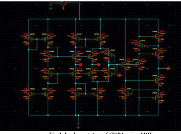
and n are ideally zero. It is implemented using MOS as shown in Fig2
Fig 2. Implementation of CDBA using MOS
It consists of a Differential Current Controlled Current Source (DCCCS) which has a finite input resistance followed by a voltage buffer. It can be operate in both voltage and current mode. In Fig 2, M1-M16 forms DCCCS circuit and MB1-MB8 forms voltage buffer circuit.
In the ideal case the transfer function of the circuit can be expressed by
𝑇(𝑆) = 𝐼𝑜𝑢𝑡𝐼𝑖𝑛 =𝑌𝑝−𝑌𝑛𝑌𝑝+𝑌𝑛 (3)
This form of 𝑇(𝑆) is suitable for first order all pass filter applications. Here the singleCDBA along with six MOS transistors is used and provides a single ended voltage output. To obtain a differential output voltage the other multiplier circuits uses t wo squaring circuits along withresistors. Here the same task is performed with only six MOSFETs and a CDBA element. Many applications are based on CDBA namely fully integrated signal process circuits, current mode filters, voltage mode filters, resistance controlled sinusoidal oscillators.
Theoretical analysis
Proposed implementation of current-mode multiplier and divider circuit is presented in Fig. 3, 4. Translinear loop is a loop that goes through only source-gate connection of MOS. Here the translinear loop exists in M1, M2, M3,and M4
The drain current is assumed to be proportional to the square of the weighted sum of the input signals which considers the squaring characteristics of MOS biased in saturation. The drain current is expressed as,
ID1,2 = I2 – (I1 ±I0) +[ (I1 ±I0)2 / 4I2] (5)
Thus the output current expression is
IOUT = ID2 – ID1 +2I0 (6)
Which results,
IOUT = I0 I1 / I2 (7)
Hence both multiplying and dividing function can be implemented, which has the advantage of independency of output current on technological parameter and it is not affected by temperature variations. For a MOS transistors mobility degradation can be modeled as
µ = µ0
(1+𝜃(𝑣𝑔𝑠−𝑣𝑡) (8)
Here 𝜃 is a mobility reduction parameter which is process dependent and may have values ranging from 0.01 to 0.25 V-1. Mobility
reduction is considered to be geometry independent and causes more problems for distortion.
Implementations and results
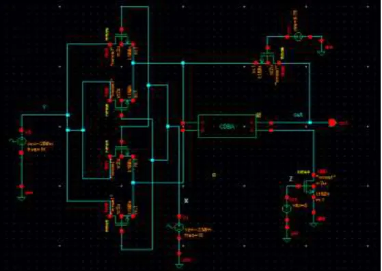
A complete multiplier and divider circuit using CDBA element is shown in Fig 3. It can be able to operate as a multiplier and the divider without changing circuit configuration. There are three input terminals in the circuit namely X, Y, Z. To operate the circuit as a multiplier, input signals are applied to X and Y terminals and the control voltage is applied to Z terminal. The input signals are varied from -0.2 mA to 0.2 mA. The control voltage Ic1 and Ic2 is 1.2 mA, 1 mA.Similarly to operate the circuit as a divider, input signals are applied to Y and Z terminal which varies from -0.2 mA to 0.2 mA and -2 mA to 2mA respectively. The control voltage is applied to X terminal and its value is similar to a multiplier. Hence by changing inputs to different terminals, two modes of operation can be done.The output current of the analog multiplier is given by
𝐼𝑜 𝑚𝑢𝑙 = (𝐼𝑐2−𝐼𝑐1)𝑥𝑦 (9)
The output voltage of the analog divider is given by
𝐼𝑜 𝑑𝑖𝑣 = (𝐼𝑐2 − 𝐼𝑐1)𝑦𝑧 (10)
The circuit configuration has independence of output from the aspect ratios of the MOSFETs if all of them are assumed to be matched. On the other hand different aspect ratios are used for input and output MOS transistors to have desired gain factor
Fig 4. Implementation of Divider circuit
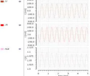
Fig 5a. Transient response for the multiplier circuit
From the Fig 5a, the output of the multiplier circuit is calculated for the corresponding inputs with respect to time
Fig 6a. Power response of the circuit From the Fig 6a, the average power consumption of the circuit is calculated.
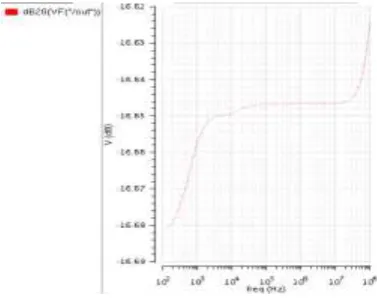
Fig 6b.dB waveform From the Fig 6b, the bandwidth of the circuit is calculated.
Table1
Comparison between the proposed multiplier/divider circuits and previous reported works
From the table of comparison, we can compare the parameters like technology, supply voltage, power consumption, and the bandwidth between the existing and the proposed techniques
Reference. No Technology
(µm)
Supply voltage (V) Power consumption (µW)
Chip area (µm2) Bandwidth (MHz)
[5] 0.8 1.75 0.2
[6] 0.35 2 5.5 18700 4.3
[8] 0.35 1.2 130
[10] 0.35 1.15 290 44.9
[14] 0.18 1.2 60 600 79.6
Conclusion
This brief presented the current-mode multiplier/divider circuit designed using Current Differencing Buffered Amplifier (CDBA). The presented structure reduces the circuit’s power consumption of about 45.67µW and improves the bandwidth of about 83.6 MHz and also simplifies the implementation. It can be able to operation the frequency range of more than 100 MHz. The proposed structure uses only six MOSFET’s along with CDBA. Implemented circuit using 180-nm CMOS technology has the advantage of realizing both multiplier and the divider in the same circuit.
Acknowledgement
The authors would like to express their thanks and gratitude to the Department of ECE, Karpagam University for the constant support and encouragement.
References
1. C. Popa, “CMOS multifunctional computational structure with improved performances,” in proc. 33th Ed. Annu. Semicond. Conf., vol. 2. 2010, pp. 471-474
2. C. Popa, “Multiplier circuit with improved linearity using FGMOS transistors,” in proc. Int. Symp. ELMAR 2009, pp. 159-162.
3. C. Popa, “Improved linearity active resistor with controllable negative resistance,” in proc. IEEE Int. Conf. Integr. Circuits Design Technol., Aug.2006, pp. 1-4.
4. Abuelma’atti, M.T. and Al- Qahtani, M.A, “A current- mode current-controlled current-conveyor based analogue multiplier/ divider,” International Journal of Electronics, 85(1). 71-77. 1998
5. Abuelma’atti, M.T. and Al- Qahtani, M.A, “A current- mode current-controlled current-conveyor based analogue multiplier/ divider,” International Journal of Electronics, 85(1). 71-77. 1998
6. M. Gravati, M. Valle, G. Ferri, N. Guerrini, and N. Reyes, “A novel current-mode very low power analog CMOS four quadrant multiplier,” in Proc. 31st Eur. Solid-state Circuits Conf., Sep 2005, pp.495-498.
7. Y. H. Kim and S.B.Park, “Four-quadrant CMOS analog multiplier,” Electron. Lett.,vol. 28, no.7, pp.649-650, Mar 1992. 8. C. Popa, “Low-power CMOS bulk-driven weak inversion accurate current-mode multiplier/divider circuits,” in proc. Int.
Conf. Electr. Electron. Eng., 2003, pp. 66-73.
9. Yuce, E, “Design of simple current-mode multiplier topology using a single CCCII+,” IEEE Transaction on Instrumentation and Measurement, 57(3). 631-637. 2008.
10. Tangsrirat, W., Pukkalanun, T., Mongkolwai, P. and Surakampontorn, W, “Simple current-mode analog multiplier, divider, square-rooter and squarer based on CDTAs,” International Journal of Electronics, 65 (3). 198-203. 2011.
11. Khachab, N. I. and Ismail, M, “MOS multiplier/divider cell for analogue VLSI,” Electronics Letters, 25(23), 1550-1551. 1989 12. AC Demartinos, C Psychalinos, “Ultra low voltage CMOS current-mode four quadrant multiplier,”Electron. Lett, vol. 2, no.
4, 2014.
13. JK Pathak, AK Singh, R Senani “New squaring and square-rooting circuits using cdba,” in American Journal of Electrical and Electronics Engineering, vol. 2, 2014
14. Amin Malekpour, Alireza Ejlali,”Improving the Energy/Power Consumption of Parallel Decimal Multipliers,”Indian Journal of Science and Technology, Volume 7, Issue 3, March 2014